

Philips N74ALS139D, N74ALS139N Datasheet
74ALS139
Dual 1-of-4 decoder/demultiplexer
Product specification 1991 Feb 08
INTEGRATED CIRCUITS
IC05 Data Handbook
Philips Semiconductors Product specification
74ALS139Dual 1-of-4 decoder/demultiplexer
2
1991 Feb 08 853–1426 01670
FEA TURES
•Demultiplexing capability
•Two independent 1-of-4 decoders
•Multi-function capability
DESCRIPTION
The 74ALS139 is a dual 1-of-4 decoder/demultiplexer. This device
has two independent decoders, each accepting two binary weighted
inputs (A
0n
, A1n) and providing four mutually exclusive active-Low
outputs (Q
0n–Q3n). Each decoder has an active-Low enable (E).
When E
is High, every output is forced High. The enable can be
used as the data input for a 1-of-4 demultiplexer application.
TYPE
TYPICAL
PROPAGATION DELAY
TYPICAL
SUPPLY CURRENT
(TOTAL)
74ALS139 6.0ns 4mA
ORDERING INFORMATION
ORDER CODE
DESCRIPTION COMMERCIAL RANGE
V
CC
= 5V ±10%,
T
amb
= 0°C to +70°C
DRAWING
NUMBER
16-pin plastic DIP 74ALS139N SOT38-4
16-pin plastic SO 74ALS139D SOT109-1
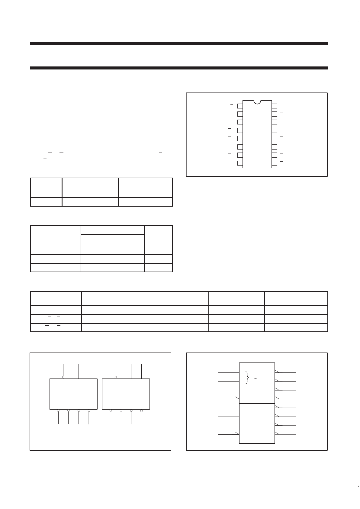
PIN CONFIGURATION
16
15
14
13
12
11
107
6
5
4
3
2
1
Q
3a
V
CC
Q0b
Q1b
Q2b
A1b
E
b
A0b
E
a
A0a
Q
2a
A1a
Q
0a
Q
1a
98GND Q3b
SF00129
INPUT AND OUTPUT LOADING AND FAN-OUT TABLE
PINS DESCRIPTION
74ALS (U.L.)
HIGH/LOW
LOAD VALUE
HIGH/LOW
A0n, A1n Address inputs 1.0/1.0 20µA/0.1mA
Ea, Eb Enable inputs (active-Low) 1.0/1.0 20µA/0.1mA
Q0n, Q1n Data outputs 20/80 0.4mA/8mA
NOTE: One (1.0) ALS unit load is defined as: 20µA in the High state and 0.1mA in the Low state.
LOGIC SYMBOL
A0a A1aEa
123
V
CC
= Pin 16
GND = Pin 8
SF00130
Q0a Q1a Q2a
456
Q3a
7
A0b A1bEb
15 14 13
Q0b Q1b Q2b
12 11 10
Q3b
9
DECODER a DECODER b
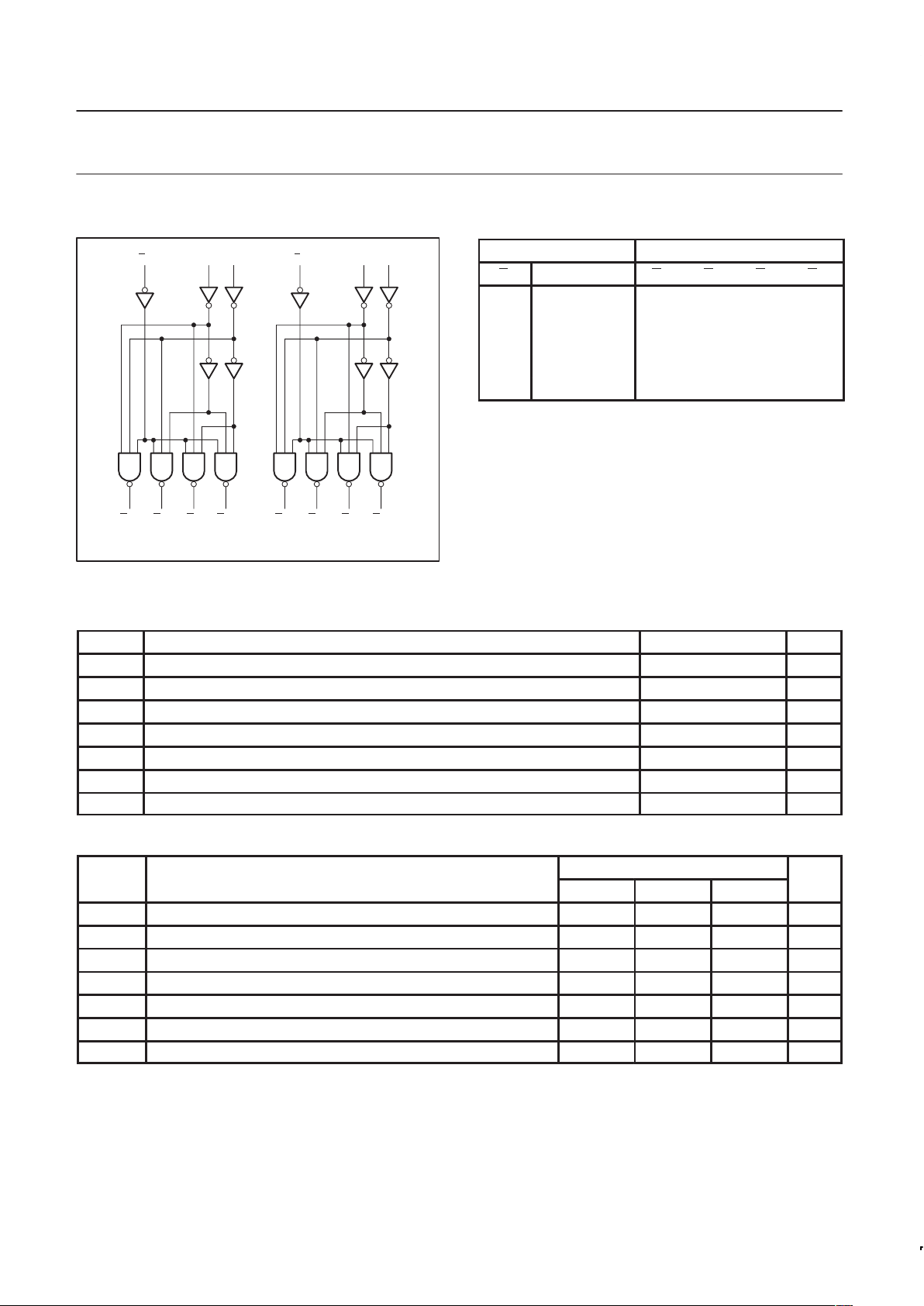
IEC/IEEE SYMBOL
SF00131
DEMUX
2
3
1
14
13
15
4
5
6
7
12
11
10
9
0
1
0
1
2
G
0
3
3
Philips Semiconductors Product specification
74ALS139Dual 1-of-4 decoder/demultiplexer
1991 Feb 08
3
LOGIC DIAGRAM
SF00132
123
E
a A0a A1a
4567
Q
0a Q1a Q2a Q3a
V
CC
= Pin 16
GND = Pin 8
15 14 13
E
b A0b A1b
12 11 10 9
Q
0b Q1b Q2b Q3b
FUNCTION TABLE
INPUTS OUTPUTS
E A0 A1 Q0 Q1 Q2 Q3
H X X H H H H
L L LLHHH
LHLHLHH
LLHHHLH
LHHHHHL
H = High voltage level
L = Low voltage level
X = Don’t care
ABSOLUTE MAXIMUM RATINGS
(Operation beyond the limit set forth in this table may impair the useful life of the device.
Unless otherwise noted these limits are over the operating free-air temperature range.)
SYMBOL
PARAMETER RATING UNIT
V
CC
Supply voltage –0.5 to +7.0 V
V
IN
Input voltage –0.5 to +7.0 V
I
IN
Input current –30 to +5 mA
V
OUT
Voltage applied to output in High output state –0.5 to V
CC
V
I
OUT
Current applied to output in Low output state 16 mA
T
amb
Operating free-air temperature range 0 to +70 °C
T
stg
Storage temperature range –65 to +150 °C
RECOMMENDED OPERATING CONDITIONS
LIMITS
SYMBOL
PARAMETER
MIN NOM MAX
UNIT
V
CC
Supply voltage 4.5 5.0 5.5 V
V
IH
High-level input voltage 2.0 V
V
IL
Low-level input voltage 0.8 V
I
Ik
Input clamp current –18 mA
I
OH
High-level output current –0.4 mA
I
OL
Low-level output current 8 mA
T
amb
Operating free-air temperature range 0 +70 °C
 Loading...