

Page 1

Service
Service
DVD Receiver
Service
Service
Service
MX3550D/37S & MX3600D/37
MX3700D/37S & MX3800D/21H/22S
Service Manual
For repair information on the Subwoofer please refer to Service
Manual of Active Subwoofer SW3600 12NC: 3139 785 30069 and
SW3700/SW3800 12NC: 3139 785 30068
TABLE OF CONTENTS
Location of PC Boards................................................1-2
Versions Variation & Package ....................................1-2
Specifications ..............................................................1-3
Measurement Setup ................................................... 1-4
Service Aids ................................................................1-5
ESD & Safety Instruction ............................................ 1-6
Setting Procedure & Repair Instructions ....................... 2
Disassembly Instructions & Service positions .............. 3
Block & Wiring Diagram ................................................ 4
Key/ Volume/ LED Board ............................................... 5
Tuner Board ...................................................................6
DVD Module: KIT572SE .......................................... 7
KIT772SI ......................................... 7A
Main Board (Include Headphone Board) ...................... 8
Scart/ RGB Board ..........................................................9
Power Board ................................................................ 10
Mechanical Exploded View & Parts List ...................... 11
Document History ........................................................ 12
Page
COMPACT
DIGITAL AUDIO
©
Copyright 2002 Philips Consumer Electronics B.V. Eindhoven, The Netherlands
All rights reserved. No part of this publication may be reproduced, stored in a retrieval system or
transmitted, in any form or by any means, electronic, mechanical, photocopying, or otherwise
without the prior permission of Philips.
Published by KC-ET0227 Service Audio Printed in The Netherlands Subject to modification
Version 1.2
CLASS 1
LASER PRODUCT
GB
3139 785 30067
Page 2

LOCATION OF PC BOARDS
POWER PCB
1-2
SCART/RGB
TUNER PCB
SERVO PCB
LED PCB
VERSION VARIATION:
Type /Versions: MX3550D MX3600D MX3700D MX3800D
Features &
Board in used
RDS function x
Progressive scan
Scart board x
RGB board x x x x x x
Power PCB (110V~127V/120V) x x x
Power PCB (220V~240V) x x x x
KEY PCB
/37S /37 /37S /21H /22S /33S /35S
MAIN PCB
PHONE
PCB
Type /Versions: MX3550D MX3600D MX3700D MX3800D
Subwoofer
SW3600/17S x x
SW3700/17S x
SW3800/00S xxx x
/37S /37 /37S /21H /22S /33S /35S
Page 3

1-3
SPECIFICATIONS
AMPLIFIER SECTION
Power Output
- Stereo mode (DIN)................................................2 x 50 W
- Surround mode (1 kHz)............................50 W RMS/channel
Total Harmonic Distortion...........10 % at rated power (1 kHz)
Frequency Response .........................180 Hz-14 kHz/±1 dB
Signal-to-Noise Ratio........................................> 65dB(CCIR)
Input Sensitivity...........................................................400 mV
DVD SECTION
Audio Performance :
Laser Type......................................................Semiconductor
Disc Diameter.........................................................12cm/8cm
Video S/N ratio...............................................65 dB/A - WTD
Audio DAC........................................................24 Bits/96 kHz
Frequency Response...........................4 Hz-20 kHz (44.1kHz)
............................................................. 4 Hz-22 kHz (48 kHz)
............................................................. 4 Hz-44 kHz (96 kHz)
Digital Output....................................SPDIF Coaxial & Optical
Distortion.........................................................0.5% (1kHz)
MP3 :
MP3 - CD bit rate......................32, 64, 96, 128, 192, 256(kbps)
MP3 - CD sampling frequencies..............32, 44.1, 48(KHz)
Recording format.......................................................JPEG
VIDEO PERFORMANCES :
Video Decoding......................................................MPEG-2
Video DAC....................................................................10 Bits
Signal System........................................................PAL/NTSC
Video Format..........................................................4:3/16:9
Composite Video Output.....................................1.0Vp-p,75
S-Video Output.............................................Y - 1.0Vp-p,75Ω
..................................................................C - 0.286Vp-p,75Ω
IR REMOTE CONTROL
Effective Range.........................................................> 8 Meter
Number of Keys................................................................45
Battery (1.5V)............................................................AA x 2
SPEAKERS
Front Speakers / Surround speaker
System............................................................2-way shielded
Impedance/ ohm................................................................8Ω
Speaker drivers..................................3" full range, 1" piezo
Dimensions (w x h x d)................... 96 mm x 155 mm x 95 mm
Weight.............................................................. 0.45 Kg/each
Center Speaker
System............................................................2-way shielded
Impedance/ ohm................................................................8Ω
Speaker drivers...................................3" full range, 1 piezo
Dimensions (w x h x d)................250 mm x 94 mm x 80 mm
Weight............................................................... 0.92 Kg/each
Ω
For /37 and /37S only
TUNER SECTION
Tuning Range................. FM 87.5 -108 MHz (100 kHz steps)
..........................................AM 530 - 1700 kHz (10 kHz steps)
26 dB Quieting Sensitivity......................................FM 20 dB
26 dB Quieting Sensitivity..............................AM 5000 uV/m
Image Rejection Ratio...........................................FM 25 dB
................................................................................AM 28 dB
IF Rejection Ratio..................................................FM 60 dB
................................................................................AM 24 dB
Signal-to-Noise Ratio..............................................FM 55 dB
................................................................................AM 35 dB
AM Suppression Ratio...........................................FM 30 dB
Harmonic Distortion...........................................FM Mono 3%
..........................................................................FM Stereo 3%
.....................................................................................AM 5%
Frequency Response.....................FM 180 Hz-10kHz/±6 dB
Stereo Separation.........................................FM 26 dB(1 kHz)
Stereo threshold..................................................FM 23.5 dB
MISCELLANEOUS / GENERAL SECTION
Power Supply Rating...........................................120V/60 Hz
Power Consumption.................................................. 250 W
Dimensions (w x h x d)............... 435 mm x 81 mm x 360mm
Weight...........................................................................5.1 kg
For /21H, /22S, /33S, /35S only
TUNER SECTION
Tuning Range................. FM 87.5 -108 MHz (50 kHz steps)
.............................................MW531 - 1602 kHz (9 kHz steps)
26 dB Quieting Sensitivity......................................FM 20 dB
26 dB Quieting Sensitivity.............................MW 5000 uV/m
Image Rejection Ratio...........................................FM 25 dB
...............................................................................MW 28 dB
IF Rejection Ratio..................................................FM 60 dB
...............................................................................MW 24 dB
Signal-to-Noise Ratio..............................................FM 55 dB
...............................................................................MW 35 dB
AM Suppression Ratio...........................................FM 30 dB
Harmonic Distortion...........................................FM Mono 3%
..........................................................................FM Stereo 3%
....................................................................................MW 5%
Frequency Response.....................FM 180 Hz-10kHz/±6 dB
Stereo Separation.........................................FM 26 dB(1 kHz)
Stereo threshold..................................................FM 23.5 dB
MISCELLANEOUS / GENERAL SECTION
Power Supply Rating.................................220 - 240V/50 Hz
Power Consumption.................................................. 160 W
Dimensions (w x h x d)............... 435 mm x 81 mm x 360mm
Weight...........................................................................7.1 kg
Page 4

1-4
AC MILLIVOL TME TER
SIGNAL GENERATORAC
OUTPUT
AUTO DISTORTION METER
AM-FM STEREO SIGNAL
GENERATOR
INPUT OUTPUT
AM SECTION
OSCIL LOSCOPE
............
............
LOOP
AM LOOP ANT
LOAD 4 OHM
INPUT
RL
DUT
AC MILLIVOL TME TER
SIGNAL GENERATORAC
OUTPUT
AUTO DISTORTION METER
AM-FM STEREO SIGNAL
GENERATOR
INPUT OUTPUT
OSCIL LOSCOPE
............
............
FM SECTION
LOAD 4 OHM
INPUT
RL
DUT
AC MILLIVOL TME TER
SIGNAL GENERATORAC
OUTPUT
AUTO DISTORTION METER
DOLBY TEST METER
INPUT OUTPUT
AUX SECTION
OSCIL LOSCOPE
............
............
LOAD 4 OHM
.......
............
DUT
INPUT
.......
............
............
.......
............
.......
AC MILLIVOL TME TER
AUTO DISTORTION METER
DVD TEST DISC
DISC SECTION
OSCIL LOSCOPE
............
............
DUT
LOAD 4 OHM
.......
............
R L C SRSLSWR L C SRSLSW
INPUT
.......
............
............
.......
............
.......
Page 5
SERVICE AIDS
1-5
Service Tools:
Universal Torx driver holder .................................4822 395 91019
Torx bit T10 150mm ...........................................4822 395 50456
Torx driver set T6-T20 .........................................4822 395 50145
Torx driver T10 extended .....................................4822 395 50423
Compact Disc:
SBC426/426A Test disc 5 + 5A ...........................4822 397 30096
SBC442 Audio Burn-in test disc 1kHz .................4822 397 30155
SBC429 Audio Signals disc .................................4822 397 30184
Dolby Pro-logic Test Disc ....................................4822 395 10216
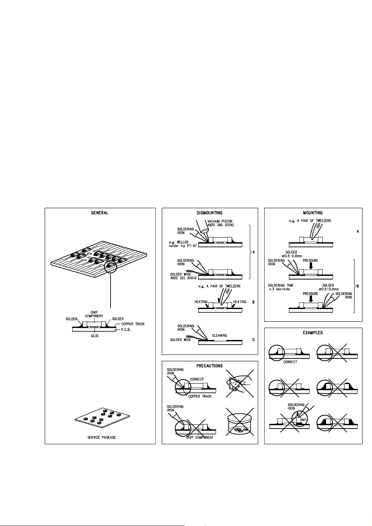
HANDLING CHIP COMPONENTS
ESD Equipment:
Anti-static table mat - large 1200x650x1.25mm ...4822 466 10953
anti-static table mat - small 600x650x1.25mm .....4822 466 10958
Anti-static wristband ............................................4822 395 10223
Connectorbox (1MΩ) ..........................................4822 395 11307
Extension cable
(to connect wristband to conn.box) ..........4822 320 11305
Connecting cable
(to connect table mat to conn.box) ...........4822 320 11306
Earth cable (to Connect product to mat or box) --4822 320 11308
Complete kit ESD3
(combining all above products) ...............4822 320 10671
Wristband tester ...................................................4822 344 13999
Page 6

WARNING
GB
All ICs and many other semi-conductors are
susceptible to electrostatic discharges (ESD).
Careless handling during repair can reduce life
drastically.
When repairing, make sure that you are
connected with the same potential as the mass
of the set via a wrist wrap with resistance.
Keep components and tools also at this
potential.
F
ATTENTION
Tous les IC et beaucoup d’autres
semi-conducteurs sont sensibles aux
décharges statiques (ESD).
Leur longévité pourrait être considérablement
écourtée par le fait qu’aucune précaution n’est
prise à leur manipulation.
Lors de réparations, s’assurer de bien être relié
au même potentiel que la masse de l’appareil et
enfiler le bracelet serti d’une résistance de
sécurité.
Veiller à ce que les composants ainsi que les
outils que l’on utilise soient également à ce
potentiel.
1-6
ESD
D
WARNUNG
Alle ICs und viele andere Halbleiter sind
empfindlich gegenüber elektrostatischen
Entladungen (ESD).
Unsorgfältige Behandlung im Reparaturfall kan
die Lebensdauer drastisch reduzieren.
Veranlassen Sie, dass Sie im Reparaturfall über
ein Pulsarmband mit Widerstand verbunden
sind mit dem gleichen Potential wie die Masse
des Gerätes.
Bauteile und Hilfsmittel auch auf dieses gleiche
Potential halten.
WAARSCHUWING
NL
Alle IC’s en vele andere halfgeleiders zijn
gevoelig voor electrostatische ontladingen
(ESD).
Onzorgvuldig behandelen tijdens reparatie kan
de levensduur drastisch doen verminderen.
Zorg ervoor dat u tijdens reparatie via een
polsband met weerstand verbonden bent met
hetzelfde potentiaal als de massa van het
apparaat.
Houd componenten en hulpmiddelen ook op
ditzelfde potentiaal.
I
AVVERTIMENTO
Tutti IC e parecchi semi-conduttori sono
sensibili alle scariche statiche (ESD).
La loro longevità potrebbe essere fortemente
ridatta in caso di non osservazione della più
grande cauzione alla loro manipolazione.
Durante le riparazioni occorre quindi essere
collegato allo stesso potenziale che quello della
massa dell’apparecchio tramite un braccialetto
a resistenza.
Assicurarsi che i componenti e anche gli utensili
con quali si lavora siano anche a questo
potenziale.
GB
Safety regulations require that the set be restored to its original
condition and that parts which are identical with those specified,
be used.
NL
Veiligheidsbepalingen vereisen, dat het apparaat bij reparatie in
zijn oorspronkelijke toestand wordt teruggebracht en dat onderdelen,
identiek aan de gespecificeerde, worden toegepast.
F
Les normes de sécurité exigent que l’appareil soit remis à l’état
d’origine et que soient utiliséés les piéces de rechange identiques
à celles spécifiées.
D
Bei jeder Reparatur sind die geltenden Sicherheitsvorschriften zu
beachten. Der Original zustand des Geräts darf nicht verändert werden;
für Reparaturen sind Original-Ersatzteile zu verwenden.
“Pour votre sécurité, ces documents
doivent être utilisés par des spécialistes agréés, seuls habilités à réparer
votre appareil en panne”.
CLASS 1
LASER PRODUCT
GB
Invisible laser radiation when open.
Avoid direct exposure to beam.
Osynlig laserstrålning när apparaten är öppnad och spärren
är urkopplad. Betrakta ej strålen.
Warning !
S
Varning !
3122 110 03420
I
Le norme di sicurezza esigono che l’apparecchio venga rimesso
nelle condizioni originali e che siano utilizzati i pezzi di ricambio
identici a quelli specificati.
"After servicing and before returning set to customer perform a
leakage current measurement test from all exposed metal parts to
earth ground to assure no shock hazard exist. The leakage current
must not exceed 0.5mA."
Varoitus !
SF
Avatussa laitteessa ja suojalukituksen ohitettaessa olet alttiina
näkymättömälle laserisäteilylle. Älä katso säteeseen!
DK Advarse !
Usynlig laserstråling ved åbning når sikkerhedsafbrydere er
ude af funktion. Undgå udsaettelse for stråling.
Page 7
2-1
2-1
System, Region code, Tuner, etc. setting procedure
1) System Reset
a) Press "SYSTEM" button on R/C. TV show "SETUP"
b) Select the menu using the "
c) Go feature setup page to do system reset
2) Region Code Change
After replacement / repair of the MPEG board, the customer
setting and the region code may lost. Changing the Region
code will put the player back in the state which it has left the
factory.
Region Code
1 USA
2EU
3 AP, Korea
4 Australia, NZ, Latam
5 RUSSIA, INDIA
6 CHINA
TV System
1 NTSC
2PAL
3AUTO
Menu/ Audio Subtitle (AS) Language
1 English
2 English
3 English
4 English
AFS
001 LX3000D/LX3500D
002
" and " " button on R/C
MX3550D/MX3600D/MX3700D/
MX3800D
Hence in total, reprograming will be done by way of the
remote control. It should run as below :-
a) Put the player in stop mode. No disc loaded.
b) Press the following key on remote control:
For MX3550D/37S (USA)
<PLAY> <159> <111> <002> <08> <PLAY>
For MX3600D/37 (USA)
<PLAY> <159> <111> <002> <08> <PLAY>
For MX3700D/37S (USA)
<PLAY> <159> <111> <002> <08> <PLAY>
For MX3800D/21H (AP)
<PLAY> <159> <331> <002> <08> <PLAY>
For MX3800D/22S (Europe)
<PLAY> <159> <221> <002> <08> <PLAY>
For MX3800D/33S (Korea)
<PLAY> <159> <311> <002> <08> <PLAY>
For MX3800D/35S (China)
<PLAY> <159> <631> <002> <08> <PLAY>
∗ After the Region Code is changed it is necessary to reset
the system so that the new Region Code will be fully
effective. All customer setting will be lost.
∗ On top of the maximum number of times allowed for
changing the region code is changed to 25.
∗ When the counter reach 25, you will not be able to further
oem derivative
08
change the code until you reset the timer by the Region
Code timer reset procedure
3) Region code change timer reset
Press below key to reset the timer :
a) In DISC source, stop mode and no disc in tray.
b) Press R/C "Play -159-PLAY" to reset timer to 25
4) Tuner area change
a) Press the "OPEN/CLOSE" button to openthe set's door
b) Press "1" "5" "9" button by using R/C.
c) TV Show "TUNER AREA ADJUST"
d) Select the tuner area you want by using the "
" button on R/C, then press "OK" to confirm. TV show
"
" TUNER AREA CHANGED"
If you didn't press it in five seconds, the system will remain
original status.
AREA BAND FREQUENCY (Hz) STEP(Hz)
USA FM 87.5M 108M 100K
AM 530K 1700K 10K
APAC FM 87.5M 108M 50K
AM 531K 1602K 9K
EUROPE FM 87.5M 108M 50K
AM 531K 1602K 9K
LATAM FM 87.5M 108M 50K
AM 530K 1710K 10K
AUSTRALIA FM 87.5M 108M 50K
/ NZ AM 531K 1602K 9K
Note :-
(a) Please refer to the above different tuner area.
" and
5. Video Out Change
a) Press "SYSTEM" on R/C button
b) Select the menu using the " " and " " button on R/C
c) Go picture setup page select Video out item.
6. Password Change
a) Press "SYSTEM" on R/C button
b) Select the menu using the " " and " " button on R/C
c) Go feature setup page select "PASSWORD". TV show
"ENTER CODE". Press 4 times of "STOP" button on R/C.
d) Select "PARENTAL" "8 ADULT" on TV.
e) Enter PASSWORD to "1234"
∗ "1234" is a default password supplied.
6. Password Change
a) Open the CD door.
b) Press "123" and "OK" on the remote control.
c) TV will show the version on screen.
7. Upgrading new software
a) Open the CD-door, then insert the CD-R program disc.
b) Close the CD-door.
c) TV will show:-
.
"disc loading"
.
"bank30.rom"
.
"writing" about 6 seconds.
.
"Done"
∗
The latest upgraded is in version VER0410.
.
region code = 1 digit
.
tv system = 1 digit
.
"as/menu lang" = 1 digit
.
"AFS" = "architechture Feature Set" = 3 digits
This field is used to define the architecture / features sets for
each product.
.
"oem derivative" = 2 digit
This field is use to define the OEM set. This will affect the
background display.
CAUTION !
This information is confidencial and may
not be distributed. Only a qualified service
person should reprogram the Region Code.
Page 8
REPAIR INSTRUCTION
2-2 2-2
Confirm Correct
Page 9
REPAIR INSTRUCTION
2-3 2-3
Page 10
3-1
3-1
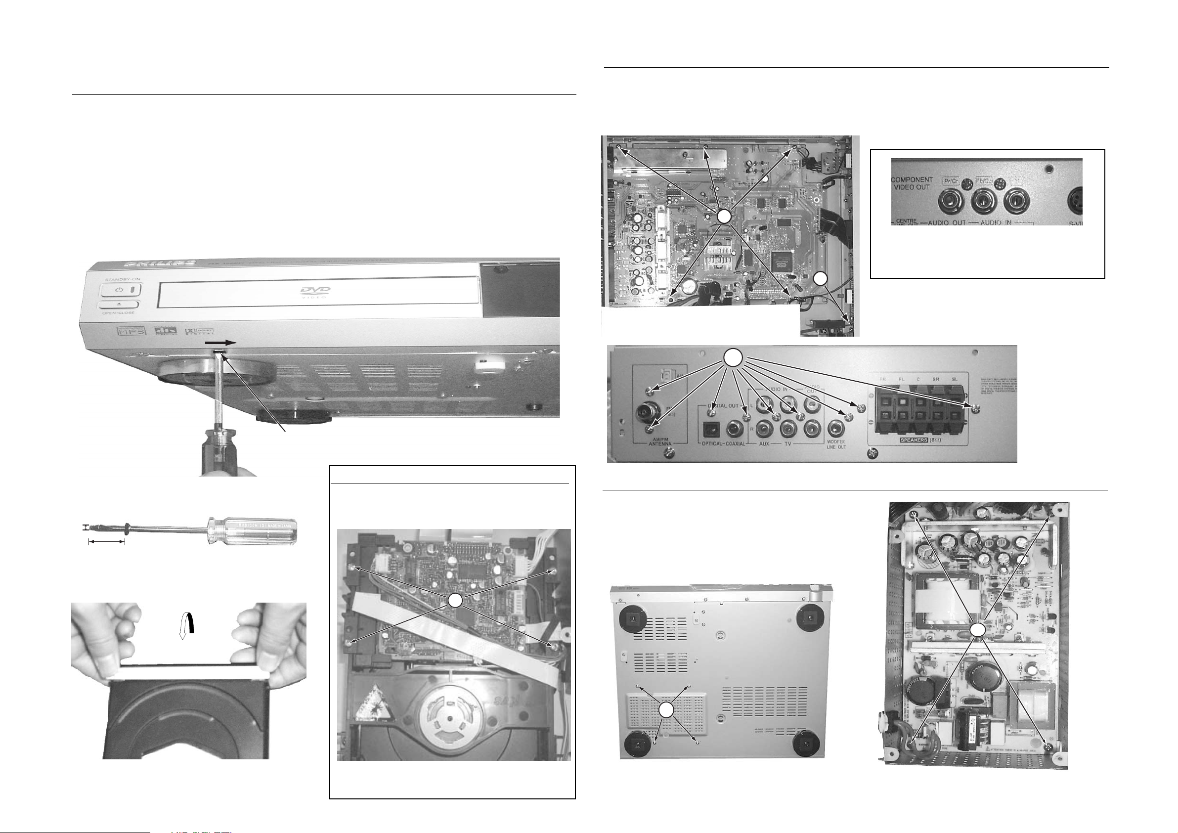
DISASSEMBLY INSTRUCTIONS
Dismantling of the Front Panel Assembly
1) Open the DVD Tray by using the Open/Close Button
while the Set is ON and disconnect the mains supply after
removing the Tray Cover.
Note: If this is not possible, the DVD T ray has to be open
manually.
Take a mini screw driver about 2mm diameter and make
a marking 24mm from the tip as shown in figure 2. place
the set on its side, insert the mini screw driver till the
marking and slide it towards the right as shown in figure
1 until the Tray moves out of the Front Panel.
RepeatRepeat
2) Return the set to its upright position and remove the Tray
Cover as shown in Figure 3 and close the tray manually
by pushing it back in.
3) Loosen 9 screws and remove the T op Cover by lifting the
rear portion upwards before sliding it out towards the rear.
-5 screws on the back
-2 screws each on the left & right side
4) Loosen 7 screws & lift up the top edge of Front Panel
assembly to free some catches before sliding it out
towards the front.
-4 screws on the bottom
-1 screw "C" on the inside as indicated in Figure 5.
-1 screw each on the left & right side
Dismantling of the Main Board
1) Loosen 5 screws "B" on the top of main board as shown in figure5.
2) Loosen 9 screws "D" at the back panel as shown in figure 6.
3) Remove all connectors on the RGBScart and main board.
B
RGB Jack use for MX3600/37 ;
MX3700/37S
Scart Jack use for MX3800/22S only
C
Figure 5
2mm
24mm
Marking just outside the slot
on the rear cabinet.
Dismantling of the Servo Board
1) Loosen 4 screws "A" to remove the Servo Board from
the DVD Module as shown in figure 4
Figure 2
D
Figure 1
Figure 6
Dismantling of the Tuner Board
1) Loosen 4 screws "E" on the bottom cover as shown in
figure 7.
3) Loosen 4 screws "F" at the top of the Power Board as
shown in figure 8
A
F
Figure 3
Note: Do not lost the limited
parts of the Servo board
Figure 4
E
Figure 7
Figure 8
Page 11
3-2
3-2
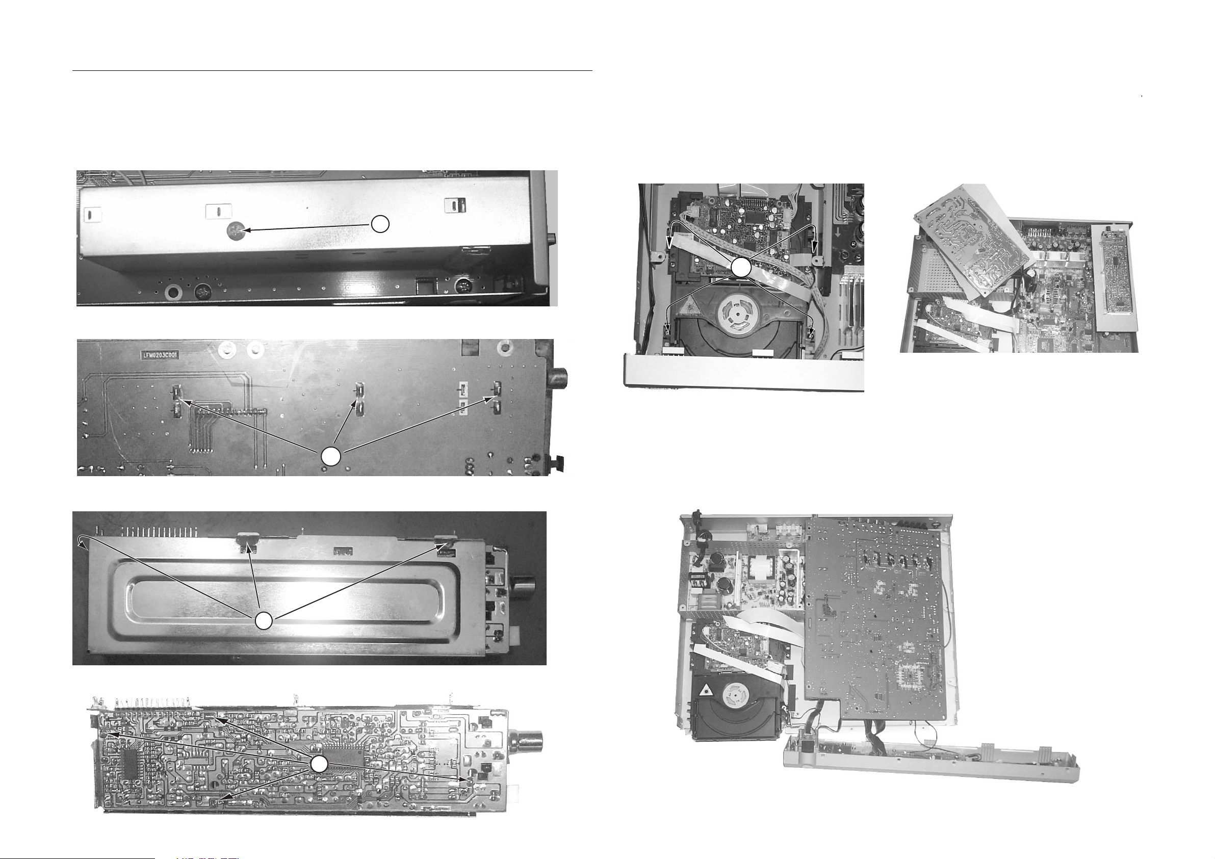
Dismantling of the Tuner PCB
1) Loosen 1 screw "G" and 3 solder points "H" to remove the
sheild cover.
2) With the Main Board already dismantle, remove the
Tuner board / sheild bracket assembly by unsolder the
wire connector and 6 points "H".
3) Separate the Tuner board by unsoldering 4 points "J".
G
Figure 9
SERVICE POSITIONS
Service position A
Loosen 4 screws "K" to remove the DVD module as shown
below
K
Service position B
Note: In some service positions the components or copper patterns of one board may risk touching its neighbouring pc
H
Figure 10
boards or metallic parts. T o prevent such short-circuit use a piece of hard paper or other insulating material between them.
Service position C
I
Figure 11
J
Figure 12
Page 12
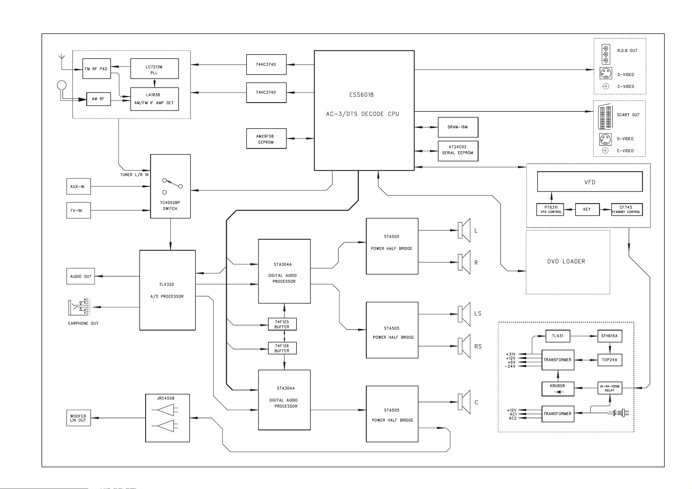
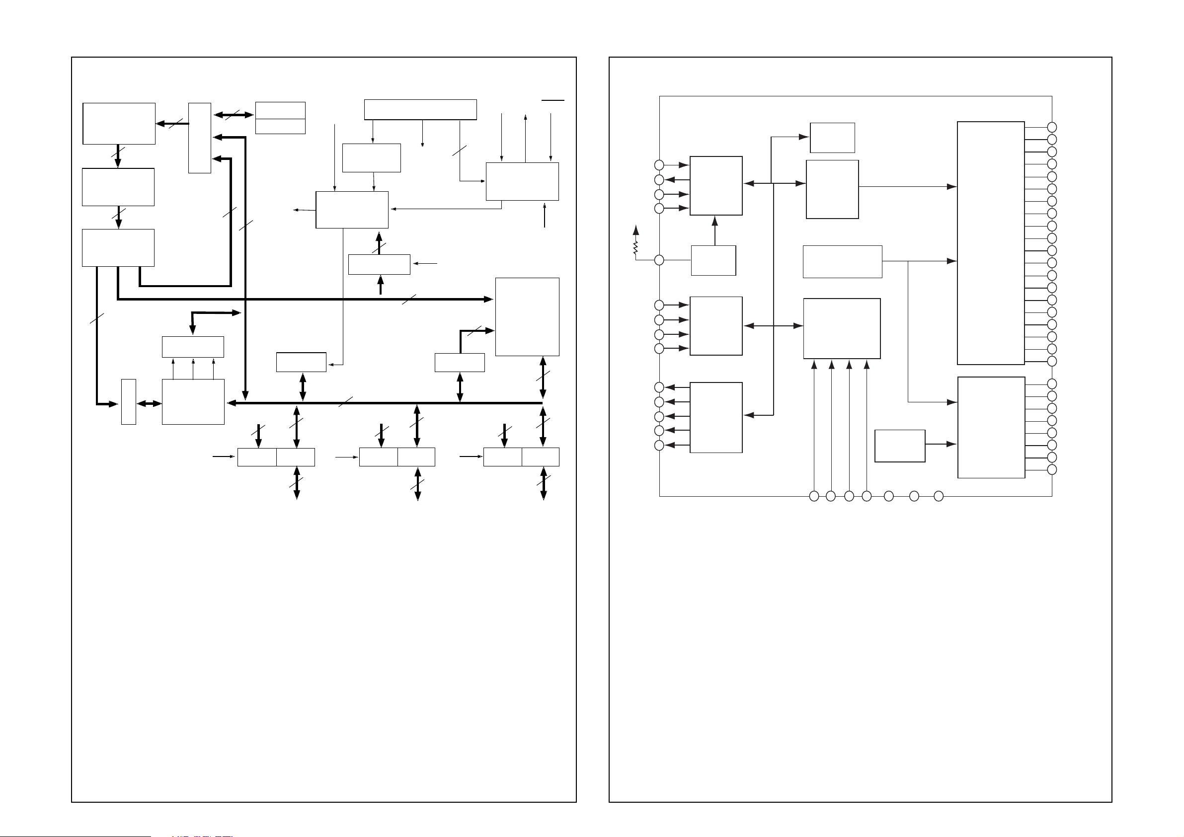
BLOCK DIAGRAM
4-1
4-1
For /37 and /37S only
For /22S only
Page 13

WIRING DIAGRAM
4-2
4-2
RGB PCB (For /37/37S only)
RB2001
SCART PCB (For /22S only)
LVA0193C001
Page 14
5-1
5-1
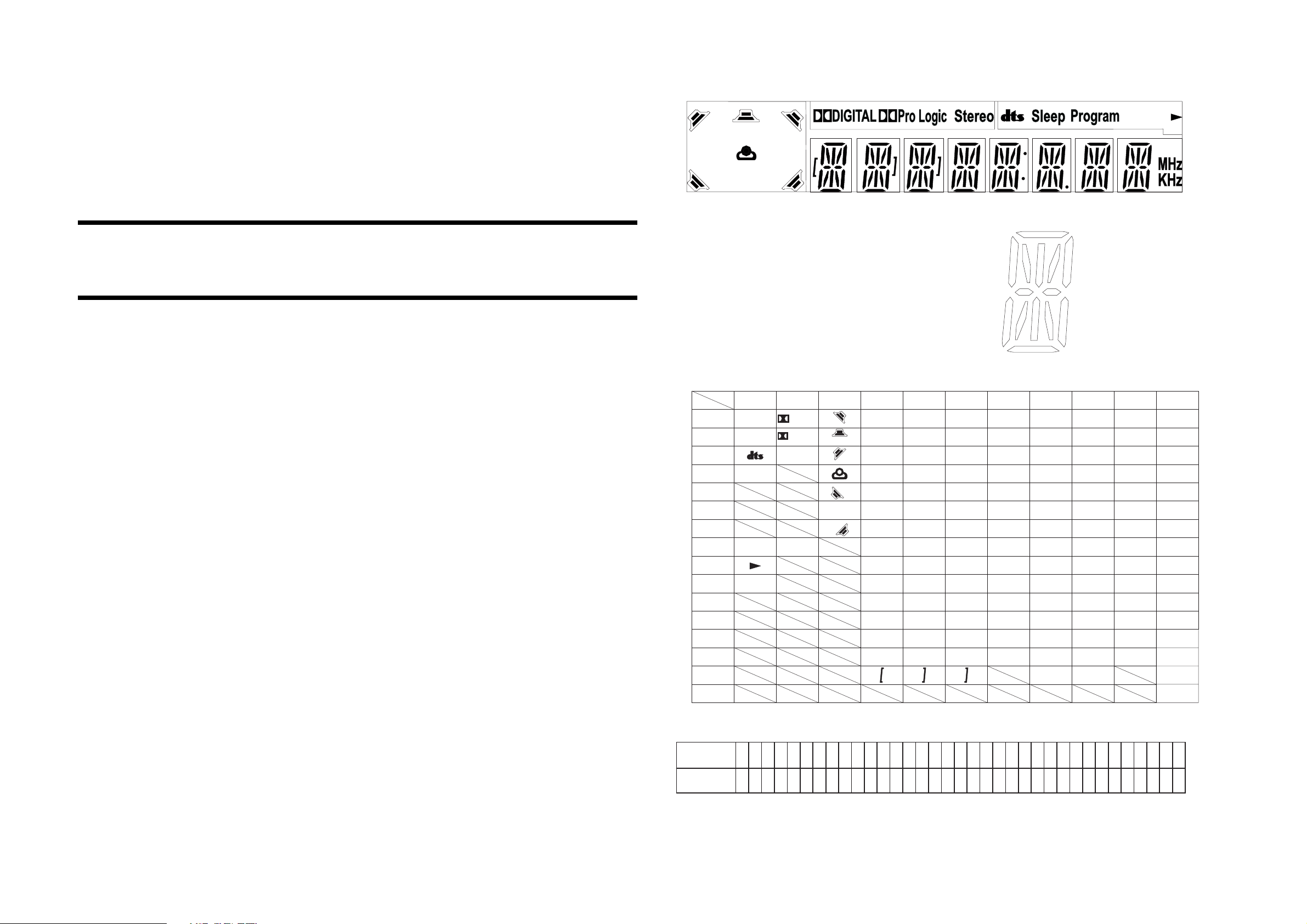
FTD DISPLAY PIN ASSIGNMENT
3G 2G 1G
KEY / VOLUME / LED BOARD
TABLE OF CONTENTS
FTD Display Pin Assignment...........................................5-1
Pin Connection ................................................................ 5-1
IC Interbnal Block Diagram ............................................. 5-2
Circuit Diagram ................................................................5-3
PCB Layout Top View ......................................................5-4
PCB Layout Bottom View ................................................5-4
Electrical Parts List ..........................................................5-5
L
SL
P1
P2
P3
P4
P5
P6
P7
P8
P9
P10
P11
P12
P13
P14
P15
P16
C
Sub
R
SR
4G 5G 6G 7G
8G 9G
f
hjk
g
r
e
(4G-11G)
1G 2G 3G 4G 5G 6G 7G 8G
Program
Sleep
DIGITAL
ProLogic
Stereo
R
Sub
SR
C
L
SL
m
a
b
h
j
k
f
g
a
b
h
j
k
f
g
m
e
r
p
n
c
d
e
r
p
n
c
d
a
b
h
j
k
f
g
m
e
r
p
n
c
d
a
b
h
j
k
f
g
m
e
r
p
n
c
d
10G 11G
a
b
m
p
n
c
d
a
b
h
j
k
f
g
m
e
r
p
n
c
d
Col
9G
a
b
h
k
f
g
m
e
r
p
n
c
d
Dp
j
10G 11G
a
b
h
j
k
f
g
m
e
r
p
n
c
d
a
b
h
j
k
f
g
m
e
r
p
n
c
d
MHz
KHz
PIN CONNECTION
1
2
3
4
PIN NO.
F
CONNECTION
## Note ##
1. Fn: Filament pin
2. nG : Grid pin
3. Pn : Anode pin
4. NP : No Pin
5. NC : No Connection pin
F
1
2
5
N
1
2
P
G
G
6
7
8
9
1
1
1
1
1
1
1
1
1
1
2
2
2
2
2
2
2
2
2
2
3
3
3
3
3
3
0
1
2
3
4
5
6
7
8
9
0
1
2
3
4
5
6
7
8
9
0
1
2
3
4
5
3
4
5
6
7
8
9
10
11
N
N
P
P
P
P
P
P
P
P
P
P
P
P
P
P
P
P
N
F
F
G
G
G
G
G
G
G
G
G
C
C
1
2
3
4
5
6
7
8
9
10
11
12
13
14
15
16
P
2
2
Page 15
5-2
CF745 INTERNAL BLOCK DIAGRAM PT6311 INTERNAL BLOCK DIAGRAM
5-2
EPROM/ROM
512 X 12 TO
2048 X 12
12
INSTRUCTION
REGISTER
12
INSTRUCTION
DECODER
8
LITERALS
W
9-11
PC
DIRECT ADDRESS
STATUS
ALU
“TRIS 5”
9-11
9
FROM W
TRISA PORTA
STACK 1
STACK 2
WDT TIME
OUT
8
DIRECT RAM
ADDRESS
4
TMR0
4
4
T0CKI
PIN
WATCHDOG
WDT/TMR0
PRESCALER
OPTION REG.
DATA BUS
8
“TRIS 6”
CONFIGURATION WORD
“DISABLE”
TIMER
“CODE
PROTECT”
CLKOUT
6
FROM W
5
FROM W
8
TRISB
8
PORTB
8
“OSC
SELECT”
2
“OPTION”
5-7
FSR
“TRIS 7”
OSC1 OSC2 MCLR
OSCILLATOR/
TIMING &
CONTROL
“SLEEP”
GENERAL
PURPOSE
REGISTER
FILE
(SRAM)
24, 25, 72 or
73 Bytes
8
FROM W
8
TRISC
8
PORTC
8
V
DD
OSC
D
D
OUT
CLK
STB
R
SW 1
SW 2
SW 3
SW 4
LED 1
LED 2
LED 3
LED 4
LED 5
SG1/KS1
Control
IN
Serial
Data
interface
Genaral
Input
Register
Segment
Driver/
Grid
Driver/
OSC
Timming
Generator
Key Scan
Output
Genaral
Input
Register
LED
Driver
Key Matrix
Memory
Grid
Driver
Dimming
Circuit
SG2/KS2
SG3/KS3
SG4/KS4
SG5/KS5
SG6/KS6
SG7/KS7
SG8/KS8
SG9/KS9
SG10/KS10
SG11/KS11
SG12/KS12
SG13/GR16
SG14/GR15
SG15/GR14
SG16/GR13
SG17/GR12
SG18/GR11
SG19/GR10
SG20/GR9
GR1
GR2
GR3
GR4
GR5
GR6
GR7
GR8
RA<3:0> RB<7:0>
RC<7:0>
(28-Pin
Devices Only)
K2 K3 K4
VEEGNDVDDK1
Page 16

CIRCUIT DIAGRAM
5-3 5-3
12 34
A
B
C
D
0V
0V
0V
0V
4.9V
4.9V
0V
5V
5V
0V
0V
0V
0V
5.1V 2.8V
0V0V0V
-20V
-21.6V
-14.6V
5.1V
-10.9V
5.1V
-21.9V
0V
5.1V
-21.9V
5.1V
-21.9V
-20.4V
-16.4V
-20.4V
-16.4V
-20.1V
5V
-20.4V
-20.4V
5V
-20.4V
-20.1V
-14.6V
-20.4V
-20.4V
-20.4V
-20.4V
-20.4V
5V
-20.4V
-20.4V
-12.9V
-9.1V
-20.1V
-22.1V
C201 A1
C202 A1
C203 A1
C204 C3
C205 C3
C207 B1
A
C208 B1
C209 B1
C212 D3
-15.6V
-15.6V
-20.4V
-20.4V
-20.4V
-20.4V
-20.4V
-20.4V
-20.4V
-20.4V
-20.4V
-20.4V
-20.4V
0V
0V
-11.6V
-7.3V
-20.4V
-21.9V
-20.0V
-12.7V
-14.5V
-0.8V
-14.5V
-21.5V
-20.0V
-20.0V
-14.5V
-12.7V
-21.9V
-21.5V
-15.5V
-15.5V
C213 D3
C214 A4
C215 A4
C295 D3
C991 D2
C992 D1
C993 D1
C994 D1
D201 C2
D202 C2
D203 C3
B
D204 B4
D985 D2
DP251 A2
IC251 B2
IC981 D2
LD20 C4
4.4V
0V
0V
Q202 C2
Q203 C2
Q204 C3
R201 A1
R202 A1
R203 A1
0V
5V
5V
C
R204 B1
R205 B1
R206 B1
R213 A1
R214 A2
R216 C3
R223 A4
R242 D3
R244 B3
R225 D3
R245 C3
R246 C3
R250 C2
R251 C2
R984 D1
R987 D1
R988 C2
R989 D2
R991 D2
R992 D2
R993 D2
R994 D2
R995 D2
RB201 B4
RB202 D3
RB203A C3
RB203B C4
RB204A C3
RB204B C4
SN201 C3
TA201 C4
TA202 C4
TA203 C1
TA204 C2
TA205 B2
TA206 C2
TA207 C2
TA208 C2
TA209 C2
TA210 C2
TA211 B4
TA212 A4
XL981 D1
ZD201 D3
ZD202 C3
ZD203 C3
R224 A4
R227 C3
R228 B1
R229 B1
R230 B1
R231 C1
R232 B4
D
R234 C2
R236 C2
R238 D1
R239 D1
R240 D1
R241 A1
12 34
Page 17
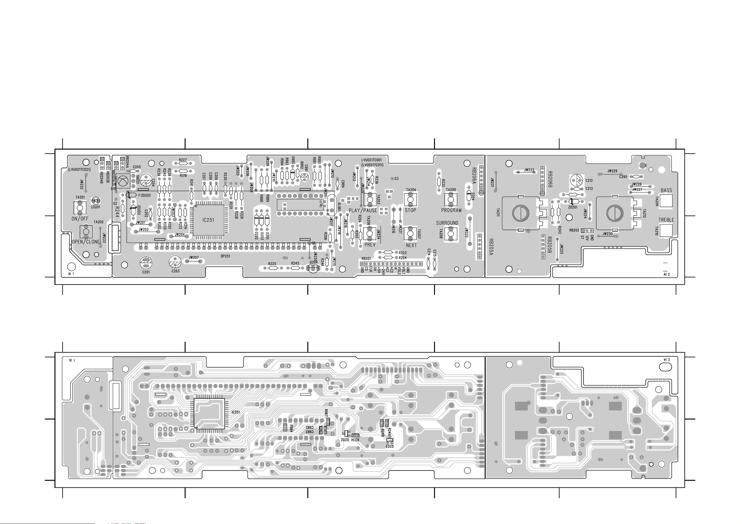
PCB LAYOUT TOP VIEW
5-4 5-4
A
B
C201 B1
C202 A1
C203 B1
C204 A1
C205 A1
C207 A2
C208 A2
C209 A2
C212 A5
C213 A5
C214 A3
C215 A4
C295 A5
C994 A3
D201 B2
D202 B2
D203 B2
D204 A4
1
D985 A2
DP251 B2
LD201 A1
JW201 B1
JW202 B1
JW203 A1
JW204 B1
JW205 A2
JW206 A2
JW207 B2
JW208 A2
JW209 A2
JW210 A2
JW211 A3
JW212 A3
JW213 A3
JW214 A3
JW215 B3
JW216 A3
JW217 B3
JW218 B3
JW219 B3
JW220 B3
JW221 A3
JW222 A4
JW223 A4
JW224 A5
JW225 B5
JW226 A5
JW227 A5
JW228 A3
JW229 A5
JW230 B5
JW231 A4
JW232 A1
JW233 B1
JW234 A3
Q204 B3
R201 A1
R202 A1
R203 A1
R204 B3
R205 B3
R206 B3
R213 A1
R214 B2
R216 A1
R223 A3
R224 A3
R225 B2
R227 A1
R228 A2
R229 A2
R230 A2
R231 A2
R232 A4
R236 A3
R238 A1
R239 A1
R240 A1
R241 A2
R242 A5
R244 A1
R245 B2
R246 B3
R988 A2
R989 A2
R991 A3
R992 A2
R993 A2
R994 A2
R995 A3
RB201 A3
RB202 B5
RB204B A1
RB203B A1
RB203A A1
RB204A A1
RB205A A4
RB205B A4
RB206A A4
RB206B A4
SN201 A1
TA201 A1
TA202 B1
TA203 A3
TA204 A3
TA205 A4
TA206 A3
TA207 A3
TA208 A4
TA209 A5
TA210 B5
TA211 A4
TA212 A5
XL981 A3
ZD201 A5
ZD202 A1
ZD203 A1
23 45
A
B
12 3 45
PCB LAYOUT BOTTOM VIEW
A
B
C992 B3
C993 B3
Q202 B3
IC251 A2
Q203 A3
R234 B3
1
R248 A3
R249 A3
R984 B2
R987 B3
23 45
A
B
12 3 45
Page 18

ELECTRICAL PARTS LIST - KEY, VOLUME & LED BOARDS
MISCELLANEOUS
SN201 9965 000 13071 IRT SENSOR IRM-2038F4 W/GND
TA201 4822 276 13648 TACT SWITCH
TA202 4822 276 13648 TACT SWITCH
TA203 4822 276 13648 TACT SWITCH
TA204 4822 276 13648 TACT SWITCH
TA205 4822 276 13648 TACT SWITCH
TA206 4822 276 13648 TACT SWITCH
TA207 4822 276 13648 TACT SWITCH
TA208 4822 276 13648 TACT SWITCH
TA209 4822 276 13648 TACT SWITCH
TA210 4822 276 13648 TACT SWITCH
TA211 9965 000 12539 ROTARY ENCODER EC16B24-204
TA212 9965 000 12539 ROTARY ENCODER EC16B24-204
XL981 9965 000 12540 CRYSTAL 4,00MHZ
CAPACITORS
C201 9965 000 14169 100uF 10V 20%
C202 4822 122 30103 22nF 80% 63V
C203 9965 000 12543 100uF 25V 20%
C204 9965 000 14169 100uF 10V 20%
C205 2038 554 00065 100nF +80/-20% Y5V 50V
C207 9965 000 12545 15pF 50V 5%
C208 9965 000 12545 15pF 50V 5%
C209 9965 000 12545 15pF 50V 5%
C212 9965 000 14169 100uF 10V 20%
C213 4822 122 30103 22nF 80% 63V
C214 9965 000 14171 27pF 50V 5%
C215 9965 000 14171 27pF 50V 5%
C217 9965 000 16685 6800pF 50V 10%
C295 5322 122 32331 1nF 10% 100V
C991 9965 000 12474 10uF /16V 20%
C992 9965 000 14150 15pF 50V 5%
C993 9965 000 14150 15pF 50V 5%
C994 9965 000 14172 47pF 50V 5%
RESISTORS
R201 4822 050 21003 10K 1% 0,6W
R202 4822 050 21003 10K 1% 0,6W
R203 4822 050 21003 10K 1% 0,6W
R204 4822 050 21001 100R 1% 0,6W
R205 4822 050 21001 100R 1% 0,6W
R206 4822 050 21001 100R 1% 0,6W
R213 9965 000 09725 4,7K 1/6W 5% CF
R214 9965 000 09727 56K 1/6W 5% CF
R216 4822 050 21001 100R 1% 0,6W
R223 4822 050 21003 10K 1% 0,6W
R224 4822 050 21003 10K 1% 0,6W
R225 9965 000 12549 220R 1/6W 5% CF
R227 4822 050 23302 3,3K 1% 0,6W
R228 4822 050 21003 10K 1% 0,6W
R229 4822 050 21003 10K 1% 0,6W
R230 4822 050 21003 10K 1% 0,6W
5-5
R231 4822 050 21003 10K 1% 0,6W
R232 4822 050 21003 10K 1% 0,6W
R234 4822 051 20223 22K 5% 0,1W
R236 4822 050 22203 22K 1% 0,6W
R238 9965 000 12515 2,2K 1/6W 5% CF
R239 9965 000 12515 2,2K 1/6W 5% CF
R240 9965 000 12515 2,2K 1/6W 5% CF
R241 4822 050 21003 10K 1% 0,6W
R242 4822 050 21502 1,5K 1% 0,6W
R244 9965 000 12630 1,2K 1/6W 5%
R245 4822 050 24703 47K 1% 0,6W
R246 4822 050 21003 10K 1% 0,6W
R248 4822 051 20008 0R JUMPER 0805
R249 4822 051 20008 0R JUMPER 0805
R250 4822 117 10837 100K 1% 0,1W
R251 4822 117 10837 100K 1% 0,1W
R984 9965 000 12484 10K 1/10W 5%
R987 4822 050 21001 100R 1% 0,6W
R988 4822 050 23302 3,3K 1% 0,6W
R989 4822 050 21003 10K 1% 0,6W
R991 4822 050 21003 10K 1% 0,6W
R992 4822 050 21003 10K 1% 0,6W
R993 4822 050 21003 10K 1% 0,6W
R994 4822 050 21003 10K 1% 0,6W
R995 4822 050 21003 10K 1% 0,6W
DIODES
D201 4822 130 30621 1N4148
D202 4822 130 30621 1N4148
D203 4822 130 30621 1N4148
D204 4822 130 30621 1N4148
D985 4822 130 30621 1N4148
DP251 9965 000 12538 VFD DISPLAY
LD201 9965 000 14174 LED 3DIA RED HI-LIGHT
ZD201 4822 130 34233 BZX79-B5V1
ZD202 4822 130 34233 BZX79-B5V1
ZD203 4822 130 34233 BZX79-B5V1
TRANSISTORS & INTEGRATED CIRCUITS
IC251 9965 000 12550 PT6311(PTC)
IC981 9965 000 14173 CF745
Q202 9965 000 14175 2SA733Q,P
Q203 9965 000 14175 2SA733Q,P
Q204 4822 130 41198 2SC945P
Note: Only the parts mentioned in this list are normal service spare
parts.
Page 19

6-1
6-1
TUNER ADJUSTMENT TABLE
Waverange Input frequency Input Tuned to Adjust Output Scope/Voltmeter
VARICAP ALIGNMENT
TUNER BOARD
TABLE OF CONTENTS
FM
87.5 - 108MHz
(50kHz grid)
AM
531 - 1602kHz
(9kHz grid)
( 22S / 30S / 21R /
21H )
AM
530-1700kHz
(10kHz grid)
( 21L / 21L / 37S )
FM - IF
FM
FM - RF
FM
AM IF
10.7MHz, 50mV
continuous wave
108MHz
87.5MHz
A
mod=1kHz
∆f= ±22.5kHz
108MHz
87.5MHz
1602KHz
531KHz
1700KHz
530KHz
IC 101
short circuit
to block AFC
108MHz
87.5MHz
5130
check
TC002
T003
1
TC002
T003
23
200P
T105
2F
6.5V ±1.2V
1.5V ±0.5V
7.8V ±0.2V
±
1.1V ±0.2V
8.0V 0.2V
1.1V 0.2V
±
fo
Symmetric
Max
MAX
Tuner Adjustment Table ..................................................................6-1
Block Diagram ................................................................................6-2
Circuit Diagram...............................................................................6-3
PCB Layout Top View..................................................................... 6-4
PCB Layout Bottom View ............................................................... 6-5
Electrical Parts List.........................................................................6-6
AM
AM AFC
MW
AM RF
MW
MW
IC 101
24
R220
100nF
T102
4
f
symmetric
max.
o
450kHz
Connect pin 29 of
IC 101 (AM Osc.)
C
∆f = ±15kHz
V
= 3mV
RF
with short wire to
ground (pin 28)
3)
1557kHz TC001
1557kHz
B
1650kHz
580kHz
∆f = ±30kHz
as low as
V
RF
possible
576kHz576kHz
1650kHz
580kHz
T002
TC001
T002
max.
4
f
o
symmetric
Use Service Testprogram. By selecting the TUNER TEST test frequencies will be stored as preset frequencies automatically.
1)
If sensitivity of frequency counter is too low adjust to max. channel separation
(input signal: stereo left 90% + 9%, adjust output on right channel to minimum)
3)
For AM RF adjustments the original frame antenna has to be used!
2)
RC network serves for damping the IF-filter while
adjusting the other one.
Page 20

BLOCK DIAGRAM
TUNER BOARD
1
ANT
AGC
3
FM FRONTEND
6-2
MIXER
7
IF OUT
6-2
FILTER LPF
1819202122239
FM IF
1
FM DET
S-CURVE
FM
AM
DECODER
STEREO
SW
4.332
VCC
46 58
FM TUNER +12V
VT
RDS IC
BU1923F
4
MUX
LPF
8th Switched
capacitor filter
5
+5V
+5V
VDD1
12
VDD2
6
VSS
REFERENCE
CLOCK
PLL 57KHz
RDS/ARI
PLL
1187 5KHz
BI-PHASE
DECODER
16
RCLK
1
QUAL
DIFFERENTIAL
13
14
DECODER
2
RDATA
OSC OUT
4.5MHz
VDD
14
1
20
15
VT
RADIO IC
LA1837
AM OSC
13
27
29
Synthesizer IC
lC7213M
12 BITS PROGRAMABLE
DIVIDER
SWALLOW COUNTER
1/16, 1/17, 4 BITS
REFERENCE
DIVIDER
POWER ON RESET
AGC
RF AMP AM MIX
24 2422 13 15
A IN
1718
IF-BUFFER
AM IF
DATA
SHIFT
REGISTER
LATCH
TUNER INDSD COMPFM LEVER
3.3K
AM DET
FILTER
PHASE DETECTOR
CHARGE PUMP
UNLOCK DETECTOR
UNIVERSAL
COUNTER
CCB
I/F
5
PD
16
3K9
11
IF IN
STEREO/MONO
9
IF REQ
8
7
6
2
3
4
AMP L-OUT
MUTE
AMP
FM
AM
CE
DI
CLK
DO
R-OUT
Page 21

CIRCUIT DIAGRAM
A
B
1234 56 789
2.4V
2.8V
2.7V
2.6V
5V
0V
0V
2.6V 0V
1234 56 789
3.1V
6-3 6-3
C001 A1
C003 A3
C005 A2
C006 C2
C007 C3
C008 B3
C009 B4
C010 B4
C011 B4
C012 B4
C013 A4
C014 A6
C015 A5
C016 A2
C101 A3
C104 A7
C105 A7
C106 A7
C107 B7
C108 A8
C109 A8
C110 A7
C111 A7
C112 C6
C113 C6
C
4
2
C114 C7
C115 C7
C116 D7
C117 D7
C118 C7
2.0V
3.6V
3.6V
3.6V
3.6V
3.4V
0V
0.4V
3.4V
2.9V
3.4V
4.3V
4.3V
4.3V
C119 D9
C120 D6
C122 D7
C123 D8
C124 D8
C125 A8
F
3.6V
9.6V
1.4V
1.1V
0V
0V
8.5V
0V
9.6V
3.6V
1
3.6V
5.1V
5V
9.6V
8.5V 4.3V
C126 A8
C127 C8
C129 A9
C130 A9
C131 A9
C132 A9
C133 A9
C134 B8
C135 B5
C136 B8
C137 C9
C138 C8
C139 C9
C140 C9
C141 D9
C142 E9
2.4V
2.4V
0V
1.8V1V1V5V2.4V0V5V
0V5V5V
4.8V0V0V
0V
2.4V
2.3V
5V
0V
0V
0V
0V
5V
C143 C6
C144 D6
C145 D7
C151 D1
C152 D1
C153 E1
C154 C2
C155 C2
C156 D2
C157 D2
C161 C3
C163 C3
C164 C3
C165 C4
C166 C4
C167 C5
C168 C5
C169 C5
C170 D3
C171 D3
C173 D4
C174 D4
CF101 A4
CF102 A5
CF103 D7
CN001 B1
D101 E7
D001 A1
D002 A1
D003 B1
D004 B1
EF001 A2
IC101 C7
IC151 D1
IC152 D4
JK001 A1
L102 A5
L103 B7
L104 D7
L151 D2
L152 E2
L153 D3
L154 E4
Q101 A4
Q102 B4
Q103 B5
Q104 B5
Q105 D8
Q001 B2
R001 B2
R002 A2
R003 C3
R004 C3
R005 B3
R006 B4
R007 A5
R008 A3
R009 A3
R101 A4
R102 A4
R103 A4
R104 A4
R105 A4
R106 A4
R107 B4
R108 B5
R109 B5
R110 C5
R112 A3
R113 B6
R114 B6
R115 A7
R116 B7
R117 D6
R118 C7
R119 C8
R122 D7
R123 E7
R124 D8
R125 D8
R126 E8
R129 B9
R130 B8
R131 B9
R132 B9
R133 D9
R134 C9
R135 E8
R136 E8
R137 C7
R138 E6
R151 D2
R154 D4
R155 C4
R156 C3
R157 C4
R158 C4
R159 C5
R160 D5
R161 D5
R162 D5
R163 D5
R165 D5
R167 E4
R168 E5
RB101 E3
T101 A7
T102 D6
T103 A9
T104 A9
T105 C7
TC001 B2
TC002 A6
T001 A2
T002 C2
T003 A6
VD001 B2
VD002 A5
VR101 B5
VR102 D8
XL151 D2
XL152 D4
Page 22

PCB LAYOUT TOP VIEW
6-4
6-4
A
C005 B5
C007 A3
C011 A2
C012 B1
C014 A4
C015 A2
C101 A5
C104 A4
C106 A4
C107 C4
C109 B4
C113 C4
C117 C4
C118 D4
C119 C1
C123 D3
C124 D3
C125 C3
C126 C3
C127 D3
C139 D3
C140 C3
C143 D4
C151 C2
C153 C2
C154 B2
C155 B2
C156 B2
C157 D2
C163 A1
C164 A1
C166 B1
C167 A3
C168 A3
C171 C1
C173 A1
C174 A1
CF101 C5
CF102 C5
CF103 D5
CN001 A6
D001 C6
D002 C6
D003 A6
D004 A6
D101 B3
J101 A5
J102 A4
J103 C4
J104 C4
J105 B4
J106 A3
J107 D3
J108 C3
J109 A2
J110 C2
J111 C2
J112 D2
J113 D2
J114 D2
J115 A2
J116 A1
J117 B1
J118 C1
J119 D1
J120 D1
J121 D1
J122 D1
J123 D1
JK001 B6
L102 A2
L103 B4
L104 D4
L151 C2
L152 D2
L153 D1
L154 D2
Q001 B5
Q104 A1
Q105 D3
Q101 B5
Q102 C5
Q103 A2
R005 B4
R007 A3
R008 B5
R104 B5
R105 C5
R108 A2
R110 D4
R123 C3
R155 B2
RB103 D6
RB101 D2
RB102A A5
T001 D5
T002 A5
T003 A4
T101 B3
T102 D5
T103 A3
T104 A3
T105 D4
TC001 A5
2C
12 345 6
B
TC002 A3
VD001 B5
VD002 A3
XL151 A2
XL152 B1
A
B
C
D
B
C
A
D
12 345 6
F24
Page 23

PCB LAYOUT BOTTOM VIEW
6-5 6-5
A
A
C001 D2
C003 A2
C006 B2
C008 B3
C009 B2
C010 B3
C013 A4
C016 B2
C105 A3
C108 B3
C110 B3
C111 B4
C112 C3
C114 C3
C115 D3
C116 D3
C120 D6
C121 C4
C122 B6
C129 B5
C130 B4
C131 A5
C132 A4
C133 B4
C134 B4
C135 B4
C136 B4
C137 D4
C138 D4
C141 D5
C142 D5
C144 D4
C145 D2
C152 C5
C161 A6
C165 A6
C169 B6
C170 C6
IC101 C3
IC151 B5
IC152 A6
R001 D2
R002 B1
R003 A2
R004 A5
R006 A5
R009 A2
R101 B2
R102 C2
R103 B2
R106 C2
R107 C2
R109 A6
R112 B3
R113 B3
R114 A3
R115 A3
R116 B3
R117 C2
R118 C3
R119 D3
R122 D6
R124 D4
R126 D4
R129 D4
R130 C4
R131 D4
R132 C4
R133 D5
R134 D5
R135 D5
R136 D5
R137 D3
R138 C6
R151 A5
R154 A6
R156 A6
R157 B6
R158 B6
R159 C6
R160 C6
R161 C6
R162 C6
R163 B6
R165 B6
R167 B6
R168 C6
VR102 D3
4C1
12 345 6
A
B
C
D
B
B
C
D
12 345 6
2 4
4
Page 24

ELECTRICAL PARTS LIST - TUNER BOARD ELECTRICAL PARTS LIST - TUNER BOARD
MISCELLANEOUS
CN001 9965 000 12565 CONNECTOR 2PIN, AM ANTENNA
EF001 9965 000 14228 FRONTEND KST-F404VA2FM /21H/22S
EF001 9965 000 12566 FRONTEND FTE3-500H /37/37S
JK001 9965 000 12567 FM ANTENNA SOCKET
XL151 9965 000 14229 CRYSTAL 4,332MHZ /22S
XL152 9965 000 14129 CRYSTAL 4,5MHZ HC-49/U
CAPACITORS
C001 2238 861 18339 33PF 1% 50V 0805
C003 9965 000 12573 0,022UF 50V 20%
C005 9965 000 12574 5PF 50V +/-0,5PF
C006 4822 126 14585 100NF 10% X7R 0805 50V
C007 2038 554 00065 100NF +80-20% Y5V 50V
C008 9965 000 12585 0,022UF 50V 10%
C009 9965 000 12573 0,022UF 50V 20%
C010 9965 000 12573 0,022UF 50V 20%
C011 4822 122 30103 22NF 80% 63V
C012 9965 000 12575 47UF 16V 20%
C013 9965 000 13454 8PF 50V 5%
C014 9965 000 12577 560PF 50V 5%
C015 4822 122 30103 22NF 80% 63V
C016 4822 126 14585 100NF 10% X7R 0805 50V
C101 4822 122 30103 22NF 80% 63V
C104 9965 000 13074 33UF 100V 20%
C105 9965 000 12573 0,022UF 50V 20%
C106 9965 000 13074 33UF 100V 20%
C107 9965 000 13075 22UF 16V 20%
C108 4822 126 14585 0,1UF 50V 10%
C109 9965 000 12580 10UF 16V 20%
C110 9965 000 12581 200PF 50V 5%
C111 9965 000 12582 30PF 50V 5%
C112 9965 000 12524 0,047UF 50V 20%
C113 9965 000 13076 47UF 16V 20%
C114 9965 000 12524 0,047UF 50V 20%
C115 9965 000 12524 0,047UF 50V 20%
C116 9965 000 12573 0,022UF 50V 20%
C117 9965 000 13076 47UF 16V 20%
C118 9965 000 12583 1UF 50V 20%
C119 9965 000 13077 1500PF 50V 10%
C120 5322 122 32658 22PF 5% 50V
C122 9965 000 12573 0,022UF 50V 20%
C123 9965 000 12583 1UF 50V 20%
C124 9965 000 12584 0,47UF 50V 20%
C125 9965 000 12580 10UF 16V 20%
C126 9965 000 12580 10UF 16V 20%
C127 9965 000 12583 1UF 50V 20%
C129 9965 000 12585 0,0022UF 50V 10%
C130 9965 000 12585 0,0022UF 50V 10%
C131 5322 126 10223 4,7NF 10% X7R 63V
C132 5322 126 10223 4,7NF 10% X7R 63V
C133 9965 000 12573 0,022UF 50V 20%
C134 9965 000 12573 0,022UF 50V 20%
C135 4822 126 13344 1,5NF 5% 63V
C136 4822 126 13344 1,5NF 5% 63V
C137 4822 126 13188 15NF 5% X7R 63V
C138 4822 126 13188 15NF 5% X7R 63V
C139 9965 000 12586 4,7UF 16V 20%
C140 9965 000 12586 4,7UF 16V 20%
C141 9965 000 12585 0,0022UF 10% 50V
C142 9965 000 14124 0,0022UF 10% 50V
C143 9965 000 14125 47UF 16V 20%
C144 9965 000 12573 0,022UF 50V 20%
C145 9965 000 12573 0,022UF 50V 20%
C151 9965 000 14227 2,2UF 16V 20% /22S
C152 5322 116 80853 560PF 5%NP0 63V /22S
C153 4822 126 13618 330PF 63V 1% /22S
C154 5322 122 32072 33PF 2%NP0 100V /22S
C155 5322 122 32072 33PF 2%NP0 100V /22S
C156 9965 000 12575 47UF 16V 20% /22S
C157 9965 000 12575 47UF 16V 20% /22S
C161 4822 126 14585 100NF 10% X7R 0805 50V
C163 9965 000 12575 47UF 16V 20%
C164 4822 122 30103 22NF 80% 63V
C165 9965 000 12588 1000PF 50V 5%
C166 9965 000 13079 3,3UF 16V 20%
C167 4822 122 30103 22NF 80% 63V
C169 9965 000 12573 0,022UF 50V 20%
C170 9965 000 12573 0,022UF 50V 20%
C171 9965 000 13076 47UF 16V 20%
C173 9965 000 12546 27PF 50V 5%
C174 9965 000 12546 27PF 50V 5%
TC001 4822 125 50692 TRIMMER 3-10PF
TC002 9965 000 14128 TRIMMER 4,2-20PF N450
RESISTORS
R001 9965 000 12591 6,8K 1/10W 5%
R002 4822 117 10837 100K 1% 0,1W
R003 4822 117 10837 100K 1% 0,1W
R004 4822 051 20102 1K 5% 0,1W
R005 9965 000 12592 330R 5% 1/6W
R006 4822 117 11373 100R 1% RC12H 0805 except /37/37S
R007 4822 050 21004 100K 1% 0,6W
R008 4822 050 21001 100R 1% 0,6W
R009 4822 051 20102 1K 5% 0,1W
R101 4822 051 20274 270K 1% 0,1W
R102 4822 051 20479 47R 5% 0,1W
R103 4822 117 13577 330R 1% RC12H 0805 1,25W
R104 9965 000 12592 330R 1/6W 5% CF
R105 4822 050 21001 100R 1% 0,6W
R106 4822 051 20274 270K 1% 0,1W
R107 4822 051 20109 10R 5% 0,1W
R108 4822 050 21003 10K 1% 0,6W
R109 4822 117 10837 100K 1% 0,1W
R110 9965 000 12593 47R 1/6W 5% CF
R112 4822 051 20332 3,3K 5% 0,1W
R113 9965 000 12484 10K 1/10W 5% /22S
R114 4822 117 13577 330R 1% RC12H 0805 1,25W
R115 4822 051 20332 3K3 5% 0,1W
R116 4822 051 20102 1K 5% 0,1W
R117 2120 108 92641 180K 1% 0,1W
R118 4822 051 20479 47R 5% 0,1W
R119 4822 051 20519 51R 5% 0,1W
R122 4822 051 20392 3K90 5% 0,1W
R123 9965 000 09725 4,7K 1/6W 5% CF
R124 4822 051 20302 3K 5% 0,1W
R125 4822 051 20102 1K 5% 0,1W
R126 9965 000 12482 47K 1/10W 5%
R129 4822 051 20472 4K7 5% 0,1W
R130 4822 051 20472 4K7 5% 0,1W
R131 9965 000 12591 6,8K 1/10W 5%
R132 9965 000 12591 6,8K 1/10W 5%
R133 4822 117 11449 2K2 5% 0,1W 0805
R134 4822 117 11449 2K2 5% 0,1W 0805
R135 9965 000 12482 47K 1/10W 5%
R136 9965 000 12482 47K 1/10W 5%
R137 4822 117 12955 2K7 5% 1/10W
R138 9965 000 12484 10K 1/10W 5%
R139 4822 051 20561 560R 5% 0,1W /21H/22S
R139 9965 000 12548 220R 5% 0,1W /37/37S
R151 4822 051 20105 1M 5% 0,1W /22S
R154 4822 051 20105 1M 5% 0,1W
R155 9965 000 12519 1K 1/6W 5% CF
R156 4822 051 20332 3K3 5% 0,1W
R157 4822 051 20102 1K 5% 0,1W
R158 4822 051 20332 3K3 5% 0,1W
R159 4822 051 20472 4K7 5% 0,1W
R160 4822 051 20472 4K7 5% 0,1W
R161 4822 051 20472 4K7 5% 0,1W
R162 4822 051 20472 4K7 5% 0,1W
R163 4822 051 20472 4K7 5% 0,1W
R165 4822 051 20472 4K7 5% 0,1W
R167 4822 051 20223 22K 5% 0,1W
R168 4822 051 20223 22K 5% 0,1W
VR102 4822 051 20392 3K9 5% 0,1W
COILS & FILTERS
CF101 4822 242 82181 CER FILTER SFE10,7MA /21H/22S
CF101 4822 242 10614 CER FILTER SFE10,7MA /37/37S
CF102 9965 000 12564 CER FILTER 10,7MHZ SFE-10,7MS
CF103 9965 000 13181 CER FILTER 450KHZ SFU450B
L102 9965 000 12568 CHOKE 10UH
L103 9965 000 15872 CHOKE 39 MH
L104 9965 000 12568 CHOKE 10UH
L151 9965 000 12568 CHOKE 10UH /22S
L152 9965 000 12568 CHOKE 10UH /22S
L153 9965 000 12568 CHOKE 10UH
6-66-6
L154 9965 000 12568 CHOKE 10UH
T001 9965 000 12597 OSC FM S-8N
T002 9965 000 15874 ANT OSC AM 4-6:10T 1-3: 86T
T003 9965 000 13081 OSC AM 108UH
T101 9965 000 12599 FILTER 78KHZ
T102 9965 000 14126 IFT AM 455KHZ
T103 9965 000 12600 FILTER 16KHZ
T104 9965 000 12600 FILTER 16KHZ
T105 9965 000 14127 FM IFT 10,7MHZ Q=60 MIN
DIODES
D001 4822 130 30621 1N4148
D002 4822 130 30621 1N4148
D003 4822 130 30621 1N4148
D004 4822 130 30621 1N4148
D101 4822 130 30621 1N4148
VD001 4822 130 81673 1SV149
VD002 4822 130 81673 1SV149
TRANSISTORS & INTEGRATED CIRCUITS
IC101 9965 000 12594 LA1837 SANYO
IC151 9965 000 12596 BU1923F /22S
IC152 9965 000 12595 LC72131M
Q001 4822 130 63173 2SK192AY
Q101 4822 130 41595 2SC1675L
Q102 4822 130 41595 2SC1675L
Q103 4822 130 63876 2SA733R
Q104 4822 130 41198 2SC945P
Q105 4822 130 41198 2SC945P
Note: Only the parts mentioned in this list are normal service spare
parts.
Page 25

7-1
WIRING CONNECTION
SLED
MOT
O
7-1
R
DVD LOADER KIT572SE
It is not recommended for component repair on this Module but
to replace the major assembly when it becomes defective.
Therefore limited service parts list are published in this
chapter.
The Circuit & Layout diagrams are published for reference
only. The repair assistance on DVD section is given on
Chapter 2.
CN900
(6P)
CN620
(2P)
(26P)
SERVO PCB
(16P)
CN600
(5P)
(11P)
(34P)
CN630
(2P)
CN510
(8P)
CN520
(4P)
LIMIT
SWITCH
SPINDLE
MOT
O
R
DVD MECHANISM
CN011
(5P)
LOARDING
MOTOR
&
LIMLT
SWITCH
TABLE OF CONTENTS
Wiring Connection ...........................................................7-1
Schematic Diagram (Top Left) .........................................7-2
Schematic Diagram (Top Right) ......................................7-3
Schematic Diagram (Bottom Left) ...................................7-4
Schematic Diagram (Bottom Right).................................7-5
Layout Diagram (Side A and B)..................................... ..7-6
Explorer View (DVD Loader).............................................7-7
Mechanical Part list..........................................................7-8
Page 26
7-2 7-2
SCHEMATIC DIAGRAM (TOP LEFT) - SERVO BOARD
Page 27

7-3 7-3
SCHEMATIC DIAGRAM (TOP RIGHT) - SERVO BOARD
Page 28

7-4 7-4
SCHEMATIC DIAGRAM (BOTTOM LEFT) - SERVO BOARD
Page 29

7-5 7-5
SCHEMATIC DIAGRAM (BOTTOM RIGHT) - SERVO BOARD
Page 30

7-6 7-6
LAYOUT DIAGRAM (DVD SIDE A)
LAYOUT DIAGRAM (DVD SIDE B)
Page 31

Exploded View - DVD Loader
i
h
f
g
e
7-7
2
p
n
b
j
a
l
d
c
k
m
o
1
3
Without DVD Drive
Page 32

MECHANICAL / ELECTRICAL PARTS LIST - DVD MODULE
1 9965 000 13082 SERVO PC BOARD ASSEMBLY
2 9965 000 13083 DVD DRIVE MECHANISM
3 9965 000 13084 LOADER MECHANISM
(without Servo
Board and DVD Drive mechanism)
c 9965 000 13085 TRAY
f 9965 000 13086 BELT
j 9965 000 13087 SWITCH LEVER
p 9965 000 13088 SPACER MECHA (SUSPENSION)
d+e 9965 000 13089 MOTOR W/PULLEY ASSEMBLY
9965 000 12822 COMPLETE DVD MODULE
(with Servo
Board and DVD Drive mechanism)
9965 000 16344 FLEX CABLE 24PIN 24CM
(for connection
between DVD's OPU and Servo Board)
Note: Only the parts mentioned in this list are normal service spare
parts.
7-8
Page 33

7A-1
WIRING CONNECTION
7A-1
DVD LOADER KIT772SI
It is not recommended for component repair on this Module but
to replace the major assembly when it becomes defective.
Therefore limited service parts list are published in this
chapter.
The Circuit & Layout diagrams are published for reference
only. The repair assistance on DVD section is given on
Chapter 2.
(2P)
CN106
(7P)
CN105
CN110
(16P)
SERVO PCB
CN109
(26P)
CN104
(6P)
CN101
(5P)
CN108
(6P)
SLEDSLED+
CN102
(6P)
CN100
(24P)
TO DVD BESE
TRAVERSE MECH.
CN002
(6P)
SP1+
SP1-
LMT
SW
DVD MECHANISM
CN001
(5P)
LOADING
MOTOR
&
LIMIT
SWITCH
TABLE OF CONTENTS
Wiring Connection ...........................................................7-1
Schematic Diagram (Top Left) .........................................7-2
Schematic Diagram (Top Right) ......................................7-3
Schematic Diagram (Bottom Left) ...................................7-4
Schematic Diagram (Bottom Right).................................7-5
Layout Diagram (Side A and B)..................................... ..7-6
Explorer View (DVD Loader).............................................7-7
Mechanical Part list..........................................................7-8
Page 34

7A-2 7A-2
SCHEMATIC DIAGRAM (TOP LEFT) - SERVO BOARD
1
RF5
TP064
000
F-
1
F+
2
T+
3
T-
4
(NC)
5
B
6
A
7
E
8
GND-PD
9
VC
10
VCC
11
F
12
D
13
C
14
CD/DVD
15
(NC)
16
(LD-CD)
17
VR-CD
18
VR-DVD
19
MD
20
LD-CD
21
HFM
22
LD-DVD
23
GND-LD
24
PICK-UP
MECHANISM
LOADING-M
M
C599
CN013
CN100
RF (NC)
GND-PD
VC
VCC
CD/DVD
MD (NC)
(LD-CD)
VR-CD
VR-DVD
DVD MD
LD-CD
HFM
LD-DVD
GND-LD
RF5
000
TP147
TP145
TP146
TP144
L1001
B
A
E
F
D
C
000
TP066
FOFO+
TO+
TO-
*
TP149
TP153
C1050
TP151
1
F-
2
F+
3
T+
4
T-
5
6
B
7
A
8
E
9
10
11
12
F
13
D
14
C
15
16
17
18
19
20
21
22
23
24
R1033
100
Q1008
2SA1037
PVR
C1004 C1005
**
C1006 C1007
0.1 0.1
TP141
TP152
TP124
470
R1034
10
TP122
10
RF5
000
TP065
TP150
C1009
1000P
Q1004
2SA1036K
R1027
R1030
R1035
3.9K
R1036
PVR
C1011
1000P
Q1005
2SA1036K
1.2K
000
TP148
10/16
C1010
C1012
10/16
22K
R1041
R1042
Q1009
*
RF5
*
R1043
R1044
*
Q1010
C1048
100P
RF5
SP1+
SP1-
*
*
DVD_CD
0.1
C1612
R1619
5.6K
RF5
R1078
R1013
FOST
DGND
000
56P
C1049
PVR
TP204
CAP
RF5
000
C1000
56P
TP200
B
000
C1001
TP201
56P
A
000
C1002
TP202
56P
D
000
C1003
TP203
56P
C
R1079
2.2M
R1004
47K
D
R1005
47K
B
R1006
C
R1007
A
R1009
R1092
10K
470P
C1008
1.2M
R1080
TOST
C1610
1000P
R1621 R1623
4.7K 10K
47K
47K
R1011
R1014
R1016
R1017
820K
R1015
2.2M
R1620
5.6K
1.2M
820K
F
R1093
E
10K
RF5
1234
BA10358
IC161
5678
DVD-KIT772SI
3.3V
*
C1040
PVR
TP250
PDRF
000
CA0
(RF)
GND
RFP
LDTH
VCC
CAN
1
CAP
2
VCC
3
PDRF
4
PD1
5
PD2
6
PD3
7
PD4
8
GND
FIN1
9
FIN2
10
*
11
*
33K
PIN1
12
PIN2
33K
TIN1
13
14
TIN2
15
LDD1
16
LDS1
LDS2
LDD2
17 18 19 20 21 22 23 24 25 26 27 28 29 30 31 32
000
AGND
AGND
D1600
R1622
4.7K
R1624
1SS355
18K
0.01
C1611
KFG
PVR
C1033
0.1
8.2K
R1062
N/C
RFN
PREF
IC100
LA9703W
LDON2
LDON2
AGOF
AGOFF
LDON1
LDON1
AGND
BCA
BCA
47/6.3
C1031
FSET
GND
GUP
WRQ
220/6.3
C1309
C1043
C1310
*
DGND
N/C
WO/*PP
LPC
VCC
C1029
0.1
C1046
SREF
TH
TP206TP205
RFN
RFP
C1027
47/6.3
(RF)
RFOP
RFON
DVD/*CD
GU
DPD/*TE
RF5
DVD_CD
WO_PP
AGND
C1045
DEFECTO
*
DVD_CD
VR
C1030
47/6.3
AGND
36K
1
49505152535455565758596061626364
PHC
XHTR
XHTR
R1061
BCAI
SREFI
ISET
WOC
PPN
RREC
TEBL
FEBL
BST
SGC
SGC
3.3V
48
47
PH
46
BH
R1056
62K
45
C1020
44
1
R1055
43
10K
C1019
42
PP
0.047
41
WO
4700P
C1018
40
TE
R1051
6.8K
39
FE
R1050
10K
38
37
CP
R1049
5.6K
36
35
FC
34
33
R1060
R1059
TP035
6.8K
6.8K
C1024
C1013
C1023
1500P
AGND
VR
R1054
TP036
100P
TP031
TP032
TP053
000 000 000 000
4700P
33K
C1017
4700P
TP033
TP052
000
R1057
6.8K
560P
C1021
TP034
TP051
TP042
56P
C1022
R1058
AGND
R1068
R1053
R1052
6.8K
VR
TBAL
FBAL
FC
BST
TP050
TP043
000
PHBCA
ADPH
VR
33K
BHC
ADBH
000
C1016
1000P
560P
C1014
TP037
C1015
R1081
1000P
TP039
WO
39K
TEC
TP038
TP040
ADRREC
ADFE
VR
ADTE
TP219
TP220
TP221
TP041
0
33K
AGND
0.1
C1041
AGND
L1002
000
5VRF5
AGND
0.1
C1042
3.3V
2.5V
L1302
000
R1339
KFG
3.3V
0.1
C1308
VR
*
C1307
0.1
AGND
FOST
TOST
FC
BST
TBAL
FBAL
SGC
SLDO
SPDO
TDO
FDO
SPD_FG
*INT_DEC
*LSI_RST
*CS_DVD
*RDY
*RD
*WR
*
C1321
0
PHBCA
ADJV
ADRREC
ADPH
ADBH
ADTE
ADFE
RFP
RFN
R1301
100K
R1302
BHC
WO
TEC
*****
C1320
C1318
C1317
C1319
**
C1400
DGND
Page 35

7A-3 7A-3
SCHEMATIC DIAGRAM (TOP RIGHT) - SERVO BOARD
3.3V
C1040
C1043
220/6.3
ADPH
ADBH
000
TP040
TP039
000
TP038
TEC
ADTE
ADFE
ADRREC
VR
*
C1309
000
TP219
000
TP220
WRQ
000
TP221
DGND
AGND
C1041
*
0.1
VR
0.1
FOST
TOST
FC
BST
TBAL
FBAL
SGC
SLDO
SPDO
TDO
FDO
C1310
AGND
AGND
L1002
000
0.1
C1042
3.3V
2.5V
KFG
3.3V
*
0.1
C1307
C1308
AGND
*
**********
C1320
C1319
C1321
SPD_FG
*INT_DEC
*RDY
*LSI_RST
*RD
*WR
*CS_DVD
5VRF5
R1301
R1302
C1318
*
C1400
L1302
PHBCA
ADRREC
100K
000
R1339
ADJV
ADPH
ADBH
ADTE
ADFE
RFP
RFN
BHC
WO
TEC
C1317
*
R1404
DGND
0
4.7K
C1316
C1322
A2.5V
C1315
C1302
R1300
C1304
C1305
C1306
C1314
0.1
*
0.1
C1313
0.1
*
C1300
VR
6.8K
R1338
1
2
3
4
5
6
7
8
9
470P
470P
0.1
C1312
C1311
D0
0.1
C1323
10
11
DGND
12
13
14
15
16
17
18
AGND
19
20
21
22
23
24
25
26
27
28
29
30
31
32
33
34
35
36
37
38
39
40
41
42
43
44
DGND
0.1
C1351
000
000
TP216
TP215
C1301
TP212
173
HFLIO
HDAT2
TP213
172
TESIO
FBUSY(RFP3)
HDAT4
HDAT3
D3
D4
TP214
000000000000
171170
BUSY(RFP2)
HDAT5
D5
XHTR
169
XHTR(RFP1)
000
HDAT6
D6
DGND
TP211
176175
174
DVSS
AD1
DVDD0
AD0
JV
RREC
RF_PH
RF_BH
TE
FE
TEST0
EFMINP
TEST1
EFMINN
SLCLPFO
SLCLPFI
SLCO1
SLCO2
AVDD1(A/DD/A)
AVSS
BHC
WO
TEC
VREF
000
TSTD1
TSTD0
F0
BST
TBAL
FBAL
SGC
SLDO
SPDO
TDO
FDO
DVDD0
DVSS
FG(PP1)
HIRQB
HWAITB
HRESB
HRDB
HCSB
HWRB
HDAT0
DVDD1
(I/O)
HDAT1
DVSS
45 46 47 48 49 50 51 52 53 54 55 56 57 58 59 60 61 62 63 64 65 66 67 68 69 70 71 72 73 74 75 76 77 78 79 80 81 82 83 84 85 86 87 88
D1
D2
MD8
MD9
MD10
MD11
MD12
MD13
MD14
MD15
000
44 43 42 41 40 39 38 37 36 35 32 31 30 29 28 27 26 25 24
I/O9
VSS
I/O15
VSS
I/O14
I/O13
I/O12
I/O11
I/O10
NC
I/O8
*MCASL
*CASL
*MCASU
*CASH
*MOE
*OE
MA8
A8A7A6
IC131
M11L416256SA
*RASNCA0A1A2
*WE
NC
MD3
MD3
NC
I/O7
MD7
MD2
158
157
MD2
MD1
MD1
*MWE
*MRAS
MD15
MD14
C1340
DVSS
MD13
0.1
153
151
152
MD15
MD14
MD13
MD0
156
155154
MD0
DVDD3(DRAM)
000
VCC
000
000
TP217
TP218
WRQ
DEFECTO
168167
DEFECTO
WRQ(RFP0)
DEFECTI(PP0)
I/O0
MD0
0
0.1
166165
DVSS
I/O1
MD1
R1334
C1341
DVDD1(I/O)
VCC
I/O6
I/O5
I/O4
I/O3
I/O2
MD4
MD3
MD2
MD7
MD6
MD5
MD4
MD5
MD6
3.3V
164
161
162
163
160159
MD6
MD7
ND5
MD4
DVDD3(DRAM)
IC130
LC78663W
000
HADR1
HADR0
HDAT7
A0
A1
D7
HADR2
A2
HADR3
A3
HADR4
A4
HADR5
A5
HADR6
A6
MWEB
*MWE
MA0
MRAS1B
MA0
*MRAS
MA1
MA1
MA2
MA2
MA3
DVDD3(DRAM)
DGND
MA3
DVSS
MA4
MA4
MA6
MA5
MA5
MA6
TP301
TP302
TP300
100/6.3
100/6.3
C1904
100/16
*
R1595
*
3.3V
RDY_HIF
C1909
R1596
HD_INT
HRST
TXD
RXD
SCLK
EMPH
C2PO
1
TP262
000
DGND
DGND
C1342
100P
000 000 000
C1910
1
2
3
4
5
6
7
R1397
10K
R1396
1K
1
2
3
4
5
6
321
IC191
54
PQ1X251M2ZP
0.1
DGND
*
IC154
CN104
5V
DGND
5V
AGND
9V_A
GND_M
C1913
DGND
14
13
12
11
10
9
8
000
1
TP261
1
*HD_INT
2
HRST
3
GND_D
4
TXD
5
RXD
6
SCLK
7
*RDY_HIF
8
GND_D
9
16M
10
GND_D
11
EMPH
12
C2PO
000
3.3V
3.3V
000
**
R1594
DGND
C1514
DGND
IC192
BA033
220/6.3
000
3.3V
6.8K
22K
R1324
TP046
R1314
000
000
C1912
0.1
C1335
220
R1411
R1335
C1333
560P
TP045
TP044
4
5
*
TP222
TP236
TP237
TP238
TP240
TP247
TP245
DGND
C1330
000
000
000
TP239
000
000
000
000
000
000
000
000
R1333
1M
IC132
C1385
AGND
TP047
22K
R1325
0.1
C1329
C1328
C1327
123
3
2
1
TC7SHU04FU
A2.5V
0.1
WO
000
ADJV
0.1
C1331
*
1.2K
0.1
0.1
DGND
000
TP260
DGND
3.3V
*
R1321
*
R1320
R1319
*
R1318
680
R1317
C1371
C1370
C1369
************
5V
9V
16M
C1368
C1367
C1366
C1365
C1903
TP263
C1364
C1363
0.1
AGND
000
0.1
C1905
C1362
C1361
*
C1999
C1360
C1900
DGND
C1902
AGND
GND_M
2.5V
16M
MA5
MA6
MA7
MA4
000
23
A4
A5
VSS
VCC
A3
2221201918171615141310987654321
MA3
MA2
MA1
MA0
MD10
MD12
MD11
MD9
146145
149148
147
150
MD9
MD11
MD12
DVSS
MD10
000
MD8
MD8
DGND
*
C1352
3.3V
15P
C1338
TP049
TP048
139138
DVDCKIO
FSEQ(FSX)
137
TEST2
000
820
R1337
136135 134
X16MIO
000 000
SPDIF
144
143
140
142141
DOUT
DVSS
DVDD1(I/O)
SYEQ(EFLG)
AVDD2(EFM/PLL)
000
HADR12
HADR9
HADR8
HADR7
MOEB
MA7
MA8
MA9
MA10
MCASLB
MCASUB
HADR11
HADR10
C2F
R1903
DGND AGND
16.9344MHZ
C1337
X1300
R1332
133
DVSS
XIN
DVSS
XOUT
DVDD2
DVDD0(2V)
VCOC
VRPFR
VPDO
AVSS
AVDD3
JVRVO
JVAIN
JVAO
JVCPC
JVCPI
AVSS
DVDFR
CDFR
FISET
PISET
FPDO
PPDO
VCOCTL
DVSS
DVDD0(2V)
EFMOUT
AVD7
AVD0
AVERRB
AVSCTB
AVDACK
000
AVACKO
AVREQI
EMPH
DVDD1
LRSY
ROMCK
ROMXA
R1904
0
15P
1M
PCN
LF3
LF2
LF1
PCK
DVSS
0
132
131
130
129
128
127
126
125
124
123
122
121
120
119
118
117
116
115
114
113
112
111
110
109
108
107
106
105
104
103
102
101
100
99
98
97
96
95
94
93
92
91
90
89
C1336
R1328
C1332
0.01
R1323
1.2K
1.8K
3.3V
C1339
0.1
*
0.1
R1322
SDT7
SDT6
SDT5
SDT4
SDT3
SDT2
SDT1
SDT0
*DERR
*DBGN
DCLK
*DACK
*DREQ
EMPH
DGND
C1334
R1331
5.6K
AGND
0.1
R1327
0.1
C1901
R1330
10K
R1329
R1326
10K
TP564
0
*
C1325
0.1
A7
A9
*MOE
A8
A10
A11
MA7
MA8
BCK
A12
C2PO
LRCK
CDDATA
Page 36

7A-4 7A-4
SCHEMATIC DIAGRAM (BOTTOM LEFT) - SERVO BOARD
SLED-M
M
SPIN-M
M
LIMIT-SW
MECHANISM
LOADING-M
M
C599
CN013
S0001
TP626
000
3.3V
TP627
5
4
3
2
1
2
3
4
5
6
10K
R1585
DGND
TP003
TP004
10K
R1586
C1600
0.1
*
000
C1609
TP063
C1512
R1583
10K
R1584
10K
0.1
3.3V
DGND
TP625
0.1
C1601
10K
R1591
*OPN_SW
*CLS_SW
TP624
TP001
R1592
10K
CN001
MLD1
MLD2
CLOSE_SW
GND_D
12345
OPEN_SW
OPEN_SW
DGND
CLOSE_SW
MLD2
MLD1
CN101
CN002
61
SLED1
5
SLED2
4
SP1+
3
SP1-
2
DGND
1
LMT_SW
CN102
000
SLED1
SLED2
SP1+
SP1DGND
LMT_SW
TP002
*LSW
SP1+
SP1-
C1602
TOTO+
FOFO+
VR
******
C1321
SPD_FG
*INT_DEC
*RDY
*LSI_RST
*RD
*WR
*CS_DVD
C1320
C1400
C1319
C1318
*
*
SP1+
SP1-
0.1
C1612
R1619
5.6K
R1620
5.6K
C1610
1000P
R1621 R1623
4.7K 10K
1234
BA10358
IC161
R1622
4.7K
18K
R1624
1SS355
D1600
C1611
0.01
C1045
AGND
KFG
TP052
TP050
TP053
TP051
000 000 000 000
5678
9V
A7
A9
A8
A6
A5
A4
9V
3.3V
12K
FWD
REV
VCC2
VLOVLO+
VO4+
VO4VO3+
VO3-
IC160
VO2+
VO2VO1+
VO1VCC1
VIN1
VIN1-A
VIN1+A
VIN1-B
R1609
10K
0.1
C1608
GND_M
000
VREF-OUT
LA6560
REG-OUT
000
000
SLDO
TP062
TP208
TP207
000000
1
2
3
4
5
6
7
8
9
10
11
12
13
14
15
16
*
17
R1608
22K
18
S-GND
VCONT
MUTE
VIN4-
VIN4+
VREF-IN
VIN1-SW
REG-IN
VIN3+
VIN3-
VIN2+
VIN2-
VIN1+B
R1618
10K
R1617
DGND
*CLOSE
*OPEN
36
35
34
VIN4
33
32
31
30
29
28
27
26
25
24
VIN3
23
22
21
VIN2
20
19
R1615
C1605
R1612
C1604
5V
0.1
C1606
R1610
12K
27K
C1603
TP209
3.6K
*
*DMUTE
*
R1614
10K
TDO
TP060
VR
TP061
R1613
10K
R1611
10K
*
TP608
FDO
SPDO
PC_TXD
PC_RXD
PC_CTS
PC_RTS
RDY_HIF
HD_INT
TP586
TP058
TP059
TP550
TP551
TP552
P76
A3
A2
A1
A0
TXD
RXD
SCLK
0.1
C1507
R1563
R1564
R1565
R1566
R1567
R1568
R1569
R1570
R1571
R1572
R1573
R1574
R1575
R1576
R1577
R1578
R1579
R1580
R1581
*
C1503
3.3K
3.3K
3.3K
3.3K
10K
10K
10K
10K
10K
10K
10K
10K
10K
33K
33K
33K
33K
33K
33K
000
TP210
0.1
C1504
10K
R1502
SPD_FG
76
77
78
79
80
81
82
83
84
85
86
87
88
89
90
91
92
93
94
95
96
97
98
99
100
*
R1503
3.3K
3.3K
3.3K
R1560
R1561
R1562
A3
A2
A1
A0
PC_TXD
PC_RXD
PC_CTS
PC_RTS
TXD
RXD
SCLK
VCC
AVCC
VREF
AVSS
VSS
*NMI
*RDY_HIF
*HD_INT
P76
P75
P74
P73
P72
P71
KEY
P67
L(L/*S)
1 2345678910111213141516171819202122232425
33K
10K
R1501
R1500
000
P67
TP057
TP505
3.3K
R1559
SPDL_FG
SPD_FG
A10
3.3K
3.3K
3.3K
3.3K
R1555
R1556
R1557
R1558
A9
A8A7A6A5A4
A10
M37911S4MHP
WRQ
*INT_DEC
*LSW
**
10K
3.3K
3.3K
R1506
R1507
R1504
R1505
WRQ
*LSW
*INT_DEC
A11
A12
3.3K
R1554
A11
A12
*OPN_SW
*CLS_SW
R1508
*CLS_SW
*OPN_SW
A15
A14
A13
3.3K
3.3K
3.3K
R1551
R1552
R1553
A13
A14
A15
IC150
P55
P57
JVMON
10K
33K
R1510
R1509
JITTER
000000
TP055TP054
TP507
A16
3.3K
R1550
A16
*DMUTE
33K
R1511
*DMUTE
TP585
33K
R1549
A17
*LSI_RST
10K
R1512
ERROR
TP553
*LSI_RST
33K
R1548
SVMON
ERRMON
10K
R1513
TP584
DECM2SVM
33K
R1547
10K
R1514
TP583
DECM1
33K
R1546
DECMON1
DECMON0
*OPEN
*CLOSE
10K
R1515
*OPEN
*CLOSE
TP582
TP056
P05
33K
R1545
P05
P47
10K
R1516
000
TP581
P46
TP509
P06
33K
R1544
P06
P46
*
R1517
TP580
P07
33K
R1543
P07
*CS_DVD
*
R1518
*CS_DVD
VSS
*ROM
3.3K
R1519
*ROM
MD1
FPRxEN
3.3K
R1520
FPRXEN
D0
3.3K
R1542
*UPDATE
10K
R1521
*UPDATE
TP566
D1
3.3K
R1541
P41
10K
R1522
P41
D2
3.3K
R1540
51525354555657585960616263646566676869707172737475
D2D1D0
(AGOFF)
DVD_CD
(DPD_TE)
(WO_PP)
FWRITER
P40
33K
R1523
P40
3.3K
R1539
LDON1
LDON2
*RESET
VCONT
33K
R1524
TP510
(BCA)
XOUT
BYTE
D4
D3
3.3K
R1538
000
D3
50
D4
49
D5
48
D6
47
D7
46
45
44
43
42
GUP
41
40
39
38
VCC
37
36
XIN
35
VSS
34
MD0
33
32
31
30
*RDY
29
*RD
28
*WR
27
26
R1537
3.3K
3.3K
3.3K
10K
10K
X1500
16MHZ
10K
3.3K
3.3K
D5
D6
D7
10K
LDON1
10K
LDON2
AGOFF
BCA
GUP
DVD_CD
DVD_CD
WO_PP
C1502
5P
C1501
5P
10K
0.1
TP513
000
*RDY
*RD
*WR
000
TP512
000
TP511
R1536
R1535
R1534
R1533
R1593
R1532
R1531
1M
R1530
R1529
C1500
R1528
R1527
R1526
000
R1525
47K
FWRITER
1
Page 37

7A-5 7A-5
SCHEMATIC DIAGRAM (BOTTOM RIGHT) - SERVO BOARD
TP580
TP582
TP581
P07P06P05
33K
33K
R1543
R1544
P07
P06
P05
P46
*CS_DVD
P47
18 19 20 21 22 23 24 25
D1
D0
3.3K
3.3K
R1542
R1541
VSS
MD1
FPRxEN
P41
*ROM
*UPDATE
D2
3.3K
R1540
5152535455565758
D2D1D0
(AGOFF)
DVD_CD
(DPD_TE)
(WO_PP)
FWRITER
P40
3.3K
R1539
LDON1
LDON2
(BCA)
XOUT
*RESET
VCONT
BYTE
************
C1315
C1314
0.1
C1313
D0
C1323
C1312
0.1
C1311
C1317
C1319
*
C1318
C1400
C1316
C1322
*
R1404
C1321
C1320
SPD_FG
*INT_DEC
*RDY
*LSI_RST
*RD
*WR
*CS_DVD
D4
D3
3.3K
R1538
D3
50
D4
49
D5
48
D6
47
D7
46
45
44
43
42
GUP
41
40
39
38
VCC
37
36
XIN
35
VSS
34
MD0
33
32
31
30
*RDY
29
*RD
28
*WR
27
26
R1531
1M
R1530
R1525
R1537
R1536
R1535
R1534
R1533
R1593
R1532
R1529
C1500
R1528
R1527
R1526
47K
3.3K
3.3K
3.3K
10K
10K
16MHZ
X1500
10K
3.3K
3.3K
D5
D6
D7
10K
LDON1
10K
LDON2
AGOFF
BCA
GUP
DVD_CD
DVD_CD
WO_PP
C1502
5P
C1501
5P
10K
0.1
TP513
*RDY
*RD
*WR
000
TP512
000
TP511
TP516
TP515
TP514
34
DVDD0
35
DVSS
36
FG(PP1)
37
HIRQB
38
HWAITB
39
HRESB
40
HRDB
41
HCSB
42
HWRB
43
HDAT0
DVDD1
44
(I/O)
HADR8
HADR7
MCASLB
MCASUB
MOEB
MA10
MA9
MA8
MA7
MA6
DVSS
DVDD3(DRAM)
MA5
MA4
MA3
MA2
MA1
MA0
MRAS1B
MWEB
HADR6
HADR5
HADR4
HADR3
HADR2
HADR1
HADR0
HDAT7
HDAT6
HDAT5
HDAT4
HDAT3
HDAT2
HDAT1
DVSS
45 46 47 48 49 50 51 52 53 54 55 56 57 58 59 60 61 62 63 64 65 66 67 68 69 70 71 72 73 74 75 76 77 78 79 80 81 82 83 84 85 86 87 88
DGND
C1344
*MCASU
C1345
**
*MCASL
C1346
*
A7
A8
TP025
3.3V
C1509
47/6.3
D1
TP005
3.3V
DGND
TP012
TP013
A3
A2A1A0
TP014
1
2
3
4
5
6
7
8
9
10
11
12
13
14
15
16
A4
A6
A5
*MWE
*
TP015
TP016
TP017
TP018
C1347
A11
A9
A8
A13
A14
NC
WE
IC151
VCC
SST39LF010
NC
A16
A15
A12
A7
A6
A5
A4 A3
*MRAS
MA0
C1343
000
MA2
MA1
MA5
MA7
MA8
MA6
MA4
MA3
*MOE
*
TP024
TP023
TP021
TP020
TP022
TP019
0.1
3.3V
C1324
OE
A10
CE
DQ7
DQ6
DQ5
DQ4
DQ3
VSS
DQ2
DQ1
DQ0
A0
A1
A2
*RD
32
A10
31
*ROM
30
D7
29
D6
28
D5
27
D4
26
D3
25
24
D2
23
D1
22
D0
21
A0
20
A1
19
A2
18
17
TP508
D2
D5D6D7
D3
D4
TP006
TP007
TP008
TP009
TP010
TP011
A11
A9
A8
A13
A14
*WR
0.1
C1508
A16
A15
A12
A7
A6
A5
A4 A3
TP026
HADR9
A9
TP027
HADR11
HADR10
A10
A11
TP028
5
4
HADR12
A12
TP029
C2F
C2PO
TP030
1
2
3
IC153
000
ROMXA
CDDATA
ROMCK
BCK
C1513
AVERRB
AVSCTB
AVDACK
AVACKO
AVREQI
LRSY
LRCK
0.01
AVD0
EMPH
DVSS
DVDD1
C1325
99
98
97
96
95
94
93
92
91
90
89
0.1
HRST
SDT3
SDT2
SDT1
SDT0
*DERR
*DBGN
DCLK
*DACK
*DREQ
EMPH
TP222
TP236
TP237
TP238
TP239
TP240
TP245
TP241
TP242
TP243
TP244
TP246
TP235
TP234
TP233
TP232
TP231
TP230
TP229
TP228
TP227
TP226
TP225
TP224
TP223
000
TP260
C1371
C1370
C1369
C1368
C1367
C1366
C1365
C1364
C1363
************
C1362
*************
C1372
C1376
C1377
C1378
C1379
C1380
C1381
C1375
C1382
C1373
C1374
C1360
C1361
C1383
C1384
RDY_HIF
16M
CDDATA
3.3V
HD_INT
HRST
SCLK
EMPH
C2PO
LRCK
SPDIF
DCLK
*DBGN
*DERR
*DACK
*DREQ
SDT0
SDT1
SDT2
SDT3
SDT4
SDT5
SDT6
SDT7
TXD
RXD
BCK
C1342
100P
R1397
10K
R1396
*UPDATE
PC_CTS
PC_RTS
PC_RXD
PC_TXD
1
*HD_INT
2
HRST
3
GND_D
4
TXD
5
RXD
6
SCLK
7
*RDY_HIF
8
GND_D
9
TP252
DGND
16M
10
GND_D
11
EMPH
12
C2PO
13
LRCK
14
BCK
15
CDDATA
16
SPDIF
CN110
26
GND
25
DCLK
24
GND
23
*DBGN
22
GND
21
*DERR
20
GND
19
*DACK
18
GND
17
*DREQ
16
GND
15
SDT0
14
GND
13
SDT1
12
GND
11
SDT2
10
GND
9
SDT3
8
GND
7
SDT4
6
GND
5
SDT5
4
GND
3
SDT6
2
GND
1
SDT7
CN109
2
DGND
1
*UPDATE
CN105
000
000
000
1K
TP251
TP254
TP255
TP253
000 000 000 000
*
*
3.3K
R1517
R1518
R1519
000
P46
TP509
*CS_DVD
TP056
*ROM
3.3K
R1520
FPRXEN
10K
R1521
*UPDATE
TP566
10K
R1522
P41
33K
R1523
P40
TP510
33K
R1524
FWRITER
MODEL NO./FACTORY MODEL NO.
DVD-KIT772SI/SS.SH
*:NO MOUNT
CHASSIS/CIRCUIT NAME
LOADER
5V
TP259
000
FWRITER
*UPDATE
FPRXEN
000 000 000
TP258
TP257
SD CODE
0SD13711122X1
TP256
LOT NO.
MK
Page 38

LAYOUT DIAGRAM ( DVD SIDE A) LAYOUT DIAGRAM ( DVD SIDE B)
7A-67A-6
CN110
CN109
TP262
TP045
R1317
R1318
R1320
R1319
TP302
R1321
R1326
R1327
C1334
C1903C1905
TP245
R1331
CN105
TP015
TP012
TP508
TP014
TP241
89
TP044
R1314
C1327
C1328
C1329
C1385
R1330
132130 120 110 100 90
L1302
C1302
C1337
C1338
DGND
TP013
C1347
C1343
88
133
R1332
R1337
AGND
R1903
R1904
C1033
R1043
R1044
L1001
TP626
R1530
R1533
R1534
CAN
R1062
Q1010
R1030
Q1005
C1011
C1009
TP627
C1513
1
IC153
X1500
2
F02 94V-0
1AD4B10D0311AA
CAN
R1027
D1600
R1623
Q1004
3
R1624
C1611
8
C1612
1
C1610
IC161
R1621
5
4
R1622
1
2
DVD
3
CD
C1512
R1591
TP063
TP124
R1592
TP122
CN102
R1619 R1620
TP516
AGND
C1601
C1609
TP515
C1030
C1043
C1027
C1031
L1002
C1046
C1029
Q1009
C1010
TP251
C1040
R1061
49
50
60
64
C1049
R1041
R1036
R1042
TP580
C1022
C1041
R1034 R1035
C1006
C1004
TP257
TP258
R1060
48 40 33
TP256
TP566
26
30
40
50
TP582
C1023
R1059
TP584
R1058
C1024
TP553
TP207
51607075
TP585
R1554
TP038
R1053
R1068
R1054
C1021
C1018
TP034
C1017
R1057
IC100
C1008
R1014
C1002
C1001
C1003
C1000
R1092
Q1008
R1033
R1078
R1079
C1007
C1005
TP209
C1012
TP208
R1513
IC150
R1555
R1556
TP061
TP033
TP221
16101
R1016
R1015
R1093
TP149
R1013
R1557
TP060
32
30
20
17
TP220
R1080
TP148
R1558
TP608
R1017
R1559
TP215
R1560
TP219
TP507
110 2025
R1561
R1562
TP218
C1321
C1320
C1319
C1318
C1317
C1316
C1315
C1314
C1313
C1312
C1311
TP062
R1339
DEFECTO
TE
TP217
C1045
TOST
FOST
IC160
GND_M
TP552
R1502
S
R1503
TP551
L
TP550
R1577
100
R1576
R1575
R1574
90
R1566
80
R1565
76
R1564
R1563
C1322
C1336
C1307
C1305
C1304
TP037
FE
AGND
TP059
R1580
R1579
R1578
TP512
TP020
TP021
TP036
C1504
TP022
C1323
C1308
TP206
TP019
C1400
R1404
C1310
R1302
R1301
RFN
TP205
RFP
DGND
C1608
C1503
DRGND
23304044
C1309
AGND
C1509
C1301
C1912
C1508
TP047
TP048
IC131
R1335
C1900
C1351
C1999
TP049
C1300
X1300
TP300
CN101
CN105
TP239
TP238
C1352
TP236
TP237
C1325
TP243
TP242
110 2022
TP046
R1324
R1325
C1330
C1331
R1322
R1323
C1332
R1328
R1329
TP301
C1902
TP232
TP230
TP228
TP226
TP224
TP235
TP233
TP229
TP227
TP225
TP246
DGND
TP222
C1367
C1368
C1371
C1369
C1370
TP244
C1361
C1365
C1362
C1363
C1364
C1366
DGND
C1333
R1411
TP234
C1335
TP231
TP223
C1904
CN104
3.3V
TP240
R1594
C1372
C1373
C1374
C1375
C1376
C1377
C1378
C1379
C1380
C1381
C1382
C1383
C1384
TP261
TP263
C1514
C1360
R1397
R1396
TP260
81014
IC154
17
R1595
R1596
F02 94V-0
1AD4B10D0311AA
5V
9V
R1583
R1586
R1585
R1584
TP255
R1522
TP008
TP007
TP006
R1545
C1019
TP204
R1005
TP203
TP065
R1523
TP513
TP010
TP009
R1539
R1538
R1543
TP043
R1055
C1020
CAN
C1042
TP200
R1004
CN100
C1500
CAN1
TP011
R1537
R1056
TP250
TP066
TP141
TP254
TP253
R1526
R1527
R1528
C1501
C1502
R1536
TP042
TP202
R1531
TP514
R1535
TP151
TP152
C1050
TP153
70
150
IC192
R1525
IC151
IC130
C1340
3.3V
C1901
TP625
C1324
60
160
C1341
TP624
TP214
C1603
R1610
R1609
C1602
R1608
C1600
TP210
R1334
TP213
TP212
C1606
TP216
TP058
11016
TP018
50
45
176
170
C1909
IC191
TP211
R1613
R1611
C1604
R1612
TP004 TP003
TP511
TP586
C1507
TP252
R1567
TP016
44403020101
C1306
TP035
R1300
C1910
C1913
TP144
TP057
R1568
TP017
TP025
R1338
R1504
R1506
R1570
R1569
TP026
TP031
TP032
TP145
TP146
R1508
TP505
R1501
R1500
TP052
TP027
R1081
C1605
R1615R1614
TP002
R1505
R1581
R1573
R1572
R1571
R1553
TP053
C1048
R1617
R1618
TP147
R1510
TP054
R1507
R1550
TP050
TP028
TP029
C1014
TP001
R1512
TP055
R1509
R1549
TP030
TP201
R1514
TP056
R1511
R1546
TP583
R1552
C1015
R1009
R1011
R1515
R1517
R1544
TP581
TP051
R1551
TP039
C1016
C1013
R1050
TP150
TP064
R1516
TP509
R1518
R1542
R1548
TP040
R1051
R1052
R1007
R1519
R1520
R1541
TP005
R1547
TP041
R1049
R1006
R1521
TP510
R1524
R1529
R1532
R1593
R1540
TP259
17203032
C1344
C1345
TP024
C1346
TP023
80
140
IC132
R1333
C1339
C1342
TP564
TP247
5V
CN101CN104
Page 39

Exploded View - DVD Loader
i
h
f
g
e
j
7A-7
2
p
n
b
a
l
d
c
k
m
o
1
Without DVD Drive
3
Page 40

MECHANICAL / ELECTRICAL PARTS LIST - DVD MODULE
1 9965 000 16291 SERVO PC BOARD ASSEMBLY
2 9965 000 16292 DVD DRIVE MECHANISM
3 9965 000 16293 LOADER MECHANISM
(without Servo
Board and DVD Drive mechanism)
c 9965 000 13085 TRAY
f 9965 000 13086 BELT
j 9965 000 13087 SWITCH LEVER
p 9965 000 13088 SPACER MECHA (SUSPENSION)
d+e 9965 000 13089 MOTOR W/PULLEY ASSEMBLY
9965 000 15489 Complete DVD MODULE KIT772SI
(with
Servo Board and DVD Drive mechanism)
9965 000 16344 FLEX CABLE 24PIN 24CM
(for connection
from DVD's OPU to Servo Board)
9965 000 16345 FLEX CABLE 6PIN 15CM
(for connection
from DVD's small pcb to Servo Board)
7A-8
Note: Only the parts mentioned in this list are normal service spare
parts.
Page 41

8-1
MAIN BOARD
8-1
6018/6028 INTERNAL IC DIAGRAM
TABLE OF CONTENTS
Internal IC Diagram ......................................................... 8-1
Circuit Diagram (Top Left) ............................................. 8-4
Circuit Diagram (Top Right).................. .......................... 8-5
Circuit Diagram (Bottom Left) ............. ........................... 8-6
Circuit Diagram ( Bottom Right) ...................................... 8-7
PCB Layout(Component View) ....................................... 8-8
PCB Layout(Copperside View)........................................8-9
Electrical Parts list .........................................................8-10
AM29F080B INTERNAL IC DIAGRAM
V
CC
V
SS
RY/BY#
RESET#
WE#
State
Control
Command
Register
PGM Voltage
CE#
OE#
VCC Detector
A0ñA19
STA304A INTERNAL IC DIAGRAM
11 10 9
Generator
Timer
SCL SDASA
Sector Switches
Erase Voltage
Generator
STB
Chip Enable
Output Enable
Logic
Y-Decoder
X-Decoder
Address Latch
STB
DQ0
ñ
DQ7
Input/Output
Buffers
Data
Latch
Y-Gating
Cell Matrix
LRCKI / SYNC
BICKI / BIT_CL
SDI_1/ SDATA_OUT
SDI_2/ SDATA_IN
RXP
RXN
RESET
29
3
4
1
2
18
19
I2S
S/PDIF
I2C
ROM
DDX
30
27
28
33
34
23
24
21
22
LEFT_A
LEFT_B
RIGHT_A
RIGHT_B
SLEFT_A
SLEFT_B
SRIGHT_A
SRIGHT_B
LFE_A
LFE_B
DSPSRC
LRCKO
43
BICKO
43
I2S
RAM
AC`97
7
PLL
14 15 43
XTI XTO
CKOUT
PowerDown
44
PWDN
SDO_1
43
SDO_2
43
SDO_3
43
EAPD
35
Page 42

8-2
8-2
STA505 AUDIO APPLICATION CIRCUIT
29
IN1A
IN1A
23
IBIAS
+3.3V
24
CONFIG
25
PWRDNPWRDN
PROTECTIONS
27
R59
10K
IN1B
C53
IN2A
IN2B
FAULT
TRI-STATE
TH_WAR
IN1B
V
DD
V
DD
V
SS
V
SS
SIGN
V
CC
SIGN
V
CC
IN2A
GND-Reg
GND-Clean
IN2B
GNDSUB
26
28
30
21
22
REGULATORS
33
34
35
36
31
20
19
32
1
&
LOGIC
M17
M15
M16
M14
TH_WAR
C58
100nF
R57
10K
C58
100nF
100nF
C60
100nF
M3
M2
M5
M4
15
17
16
14
12
11
10
13
7
8
9
6
4
3
2
5
1A
V
CC
C30
1F
OUT1A
OUT1A
GND1A
1B
V
CC
OUT1B
OUT1B
GND1B
2A
V
CC
C32
1F
OUT2A
OUT2A
GND2A
2B
V
CC
OUT2B
OUT2B
GND2B
C31
1F
C33
1F
L18 22H
100nF
C52
330pF
R63
20
100nF
L19 22H
L113 22H
100nF
C109
330pF
R104
20
100nF
L112 22 H
C20
R98
6
R100
6
C21
C110
R103
6
R102
6
C111
C99
100nF
C23
470nF
C101
100nF
C107
100nF
C108
470nF
C106
100nF
+V
CC
C55
1000F
TLV320A INTERNAL IC DIAGRAM
AVDD
1.0X
50 k
VMID
AGND
MICBIAS
RLINEIN
MICIN
LLINEIN
HPVDD
HPGND
RHPOUT
ROUT
LOUT
LHPOUT
XTI/MCLK
XTO
CLKOUT
50 k
12 to –34.5 dB,
1.5 dB Steps
10 k
VMID
12 to –34 dB,
1.5 dB Steps
Headphone
Driver
Headphone
Driver
1.0X
1.0X
1.5X
50 k
6 to –73 dB,
1 dB Steps
6 to –73 dB,
1 dB Steps
OSC
VADC
VDAC
VMID
Bypass
Mute
Line
Mute
Line
Mute
Bypass
Mute
TLV320AIC23
MUX
Mute,
0 dB, 20 dB
2:1
MUX
CLKIN
Divider
(1x, 1/2x)
CLKOUT
Divider
(1x, 1/2x)
DSPcodec
2:1
VADC
Side Tone
Mute
VDAC
–
ADC
–
ADC
–
DAC
–
DAC
Control
Interface
Digital
Filters
Digital
Audio
Interface
CS
SDIN
SCLK
MODE
DVDD
BVDD
DGND
LRCIN
DIN
LRCOUT
DOUT
BCLK
.
Page 43
8-3 8-3
g
g
g
g
g
g
g
g
g
g
g
g
g
g
g
g
(
(
)
VOLTAGES
IC100 IC501
PIN No. 1234567891011121314151617181920 PIN NO. 1 2 3 4 5 6 7 8 9 10 11 12 13 14
Volta
PIN No. 21 22 23 24 25 26 27 28 29 30 31 32 33 34 35 36 37 38 39 40
Voltage 1.4 2.1 0 0 1.9 1.7 1.4 2.1 0 0 5 1.3 1.6 0.6 0.8 0 3.2 3.3 0 0 IC502
IC102 Voltage 1.1 1.1 1.7 1.7 1.7 0 3.5 0 4.1 3.5 0 0 3.5 1.6 1.6 0 3.5 0 0 0
PIN No. 1 2 34567891011121314151617181920
Volta
IC103 Voltage 0.2 0.2 0.2 0.2 0 3.5 0.2 0.2 0.2 0.2 0 3.5 0.2 1.2 0 1.7 1.4 1.4 0 0
PIN No. 1234567891011121314151617181920 PIN No. 41 42 43 44
Volta
PIN No. 21 22 23 24 25 26 27 28 29 30 31 32 33 34 35 36 37 38 39 40
Volta
PIN No. 41 42 43 44 45 46 47 48 49 50 51 52 53 54 55 56 57 58 59 60 PIN No. 1 2 3 4 5 6 7 8 9 10 11 12 13 14 15 16 17 18 19 20
Volta
PIN No. 61 62 63 64 65 66 67 68 69 70 71 72 73 74 75 76 77 78 79 80 PIN No. 21 22 23 24 25 26 27 28 29 30 31 32 33 34 35 36
Volta
PIN No. 81 82 83 84 85 86 87 88 89 90 91 92 93 94 95 96 97 98 99 100
Volta
PIN No. 101 102 103 104 105 106 107 108 109 110 111 112 113 114 115 116 117 118 119 120 PIN No. 1 2 3 4 5 6 7 8 9 10 11 12 13 14 15 16 17 18 19 20
Volta
PIN No. 121 122 123 124 125 126 127 128 129 130 131 132 133 134 135 136 137 138 139 140 PIN No. 21 22 23 24 25 26 27 28 29 30 31 32 33 34 35 36
Volta
PIN No. 141 142 143 144 145 146 147 148 149 150 151 152 153 154 155 156 157 158 159 160
Volta
PIN No. 161 162 163 164 165 166 167 168 169 170 171 172 173 174 175 176 177 178 179 180 PIN No. 1 2 3 4 5 6 7 8 9 10 11 12 13 14 15 16 17 18 19 20
Volta
PIN No. 181 182 183 184 185 186 187 188 189 190 191 192 193 194 195 196 197 198 199 200 PIN No. 21 22 23 24 25 26 27 28 29 30 31 32 33 34 35 36 37 38 39 40
Volta
PIN No. 201 212 203 204 205 206 207 208 PIN No. 41 42 43 44
Voltage 2.3 1.1 1.1 1.1 0.2 2.1 1.3 0 Voltage 0 3.5 1.9 3.5
( AM29F )
e 1.2 2.1 0 0 1.8 0 1.3 1.7 3.3 5.1 0 5.1 0 1.9 0 1.5 1.5 1.8 1.6 1.6 Voltage 0 1.1 1.21 0 1.1 1.1 0 1.7 1.7 0 1.7 1.7 0 3.5
PIN No. 1 2 3 4 5 6 7 8 9 10 11 12 13 14 15 16 17 18 19 20
( 74HC3740 )
e0 5.1 1.5 1.1 5 5 1.2 1.9 5 0 3.3 500.9 5 5 0.6 0 5.1 5 IC502
PIN No. 21 22 23 24 25 26 27 28 29 30 31 32 33 34 35 36 37 38 39 40
( ES6018 )
e 3.3 1.7 1.6 1.7 1.5 1.6 2 0 2.6 2 2 1.7 1.4 1.4 1.9 1.1 0 3.4 1.6 2.1 Voltage 0 0 0 0
e 1.2 0.4 0.4 5 0 0 3.4 1.6 1.1 1.7 0.7 1.7 1.1 0 2.6 1.2 1.1 1.5 1.7 1.7 IC503
e 1.7 0 0 2.6 0.2 0.2 0.2 0 2.1 1.5 3.4 0 0.1 0.6 0.6 1.5 1.5 1.6 3.4 0 Voltage 0 2.2 2.2 30.5 0 0 30.5 2.2 2.2 2.2 2.2 30.5 0 0 30.5 2.2 2.2 0 0 0
e 1.5 1.5 1.5 0 0.2 0.2 0 3.4 3.3 3.4 0 3.3 0.2 0 3.3 0 1.2 1.2 1.5 1.4 Voltage 4.8 4.8 3.5 0 3.5 3.5 3.5 3.5 0.2 0.2 0.2 0.2 25.3 25.3 30.5 30.5
e 1.4 1.3 2.5 0 1.3 1.2 0 1.3 1.4 1.2 0 3.4 0.1 0.1 1.5 1.4 0 0 3.4 3.1 IC504
e0 1.3 0 3.4 1.4 1 1.3 1.3 1.9 1.2 3.3 0 0.9 0.5 0 0.5 0.2 0.3 0.4 0 Voltage 0 2.2 2.2 30.5 0 0 30.5 2.2 2.2 2.2 2.2 30.5 0 0 30.5 2.2 2.2 0 0 0
e 2.6 0 0 0 3.3 0 3.3 0 0 3.4 3.4 3.3 0 0 3.4 0.1 0 0 2.6 0 Voltage 4.8 4.8 3.5 0 3.5 3.5 3.5 3.5 0.2 0.2 0.2 0.2 25.3 25.3 30.5 30.5
e0 3.3 3.3 3.3 3.3 1.2 0 3.4 0 3.3 0 0.2 0.2 0.2 0.3 0 3.4 0.1 3.3 4.1 IC505
e 5.1 1 3.3 5.1 3 5.1 5 5.1 5.1 3.3 0 2.6 3.3 3.3 3.3 3.3 0 2.3 1.3 1.9 Voltage 1.2 0 1.7 1.7 3.5 0 3.5 0 3 3.5 0 0 3.4 1.6 1.8 0 3.5 0.9 0.9 0
e 1.4 1.2 3.4 0 0.9 0.5 0.6 1 1.4 1.2 1.3 1.4 0 3.4 0.9 1.1 1.1 3.3 3.3 0 Voltage 0.2 0 0 0 0 0 0 0.2 0.3 0.3 0 3.5 0 0 0 0 0 0 0 0
( F4LVT125 )
( STA304A )
( STA304A )
( STA505 )
( STA505 )
( STA304A )
IC104 IC506
PIN No. 1234567891011121314151617181920 PIN No. 1 2 3 4 5 6 7 8 9 10 11 12 13 14 15 16 17 18 19 20
Volta
IC105 Voltage 4.8 4.8 3.5 0 3.5 3.5 3.5 3.5 0.2 0.2 0.2 0.2 25.3 25.3 30.5 30.5
PIN No. 12345678
Voltage 00004.1005.1 IC900 Q403 Q907
IC106 Voltage 6.3 0 5.1 Voltage 0.7 0 0 Voltage 11.2 11.2 10.5
PIN No. 1234567891011121314151617181920
Volta
PIN No. 21 22 23 24 25 26 27 28 29 30 31 32 33 34 35 36 37 38 39 40 PIN No. 1 2 3 PIN No 1 2 3 PIN No. 1 2 3
Volta
PIN No. 41 42 43 44 45 46 47 48 49 50 51 52 53 54
Voltage 0 1.2 3.4 1.2 1.2 0 1.2 1 1.6 3.4 1.6 0 1.6 0 Q101 Q900 Q908
IC400 Voltage 3.3 3.3 2.6 Voltage 0 5 0 Voltage 0.7 0 0
PIN No. 12345678910111213141516
Voltage 00000005.15.10000005.1 Q903 Q909
IC401 Voltage 0 7.7 0 Voltage 5 2 5.1 Voltage 6.1 6 5.3
PIN No. 12345678
Voltage 0 0 0 -5.2 0 0 0 5.1 Q400 Q904 Q909
IC402 Voltage 1.8 5.1 1.4 Voltage 0 11.2 0 Voltage 6.3 6.2 5.6
PIN No. 1234567891011121314151617181920
Volta
PIN No. 21 22 23 24 25 26 27 28 PIN No. 1 2 3 PIN No 1 2 3 PIN No. 1 2 3
Voltage 0 0 3 3.5 1.6 0.4 3.4 0 Voltage 0.7 0 0 Voltage 11.2 0.1 11.2 Voltage 0 3.4 0
( 74HC3740 )
e0 5.1 1.4 1.3 0 0 0 1.5 5 0 3.3 5.1 0.9 1.1 0 5.1 1 1.3 0 5 Voltage 0 2.2 2.2 30.5 0 0 30.5 2.2 2.2 2.2 2.2 30.5 0 0 30.5 2.2 2.2 0 0 0
PIN No. 21 22 23 24 25 26 27 28 29 30 31 32 33 34 35 36
( AT24C02 )
PIN No. 1 2 3 PIN No 1 2 3 PIN No. 1 2 3
(4X16Y3VTW)
e 3.4 1.1 3.4 1.2 1.4 0 1.3 1.2 3.4 1.2 1.2 0 1.2 3.4 0.1 3.1 3.1 3.1 2.9 0.2 IC901 Q404 Q907
e 0.1 0.2 0.1 0.6 0.6 1.5 3.4 0 1.6 1.8 1.6 1.4 1.2 0 0.2 0.2 3.4 1.4 0.1 0 Voltage 6.2 0 5.1 Voltage 3.7 4.4 3.7 Voltage 11.3 11.2 10.5
PIN No. 1 2 3 PIN No 1 2 3 PIN No. 1 2
( TC4052BP )
Q102 (2SX945P)
PIN No. 1 2 3 PIN No 1 2 3 PIN No. 1 2 3
( 4558 )
PIN No. 1 2 3 PIN No 1 2 3 PIN No. 1 2 3
( TLV320A )
e 3.4 1.6 1.7 1.1 1.7 1.4 1.7 3.4 1.7 1.7 001.7 3.4 0 1.7 0 0.1 1.7 1.7 Q401 Q905 Q2007
( STA505 )
( BA05T )
( BA05T )
( 23C2001L)
(2SC945P)
(2SC2878-A)
2SC2878-A
(2SA733QP)
(2SC945P)
(2SA733QP)
(2SS945P)
(2SA733QP)
2SB772P/Q
( B772-P )
(2SC945P)
2SB772P/Q
( B772-P )
(2SC945P)
IC500 Q402 Q906
PIN No. 1234567891011121314 PIN No. 1 2 3 PIN No 1 2 3
Voltage 0 1.4 1.2 0 0 1.2 0 3.5 5.1 3.5 0 0 0 3.5 Voltage 0.7 0 0 Voltage 0.7 0 0
( F4LVT126)
(2SC2878-A)
(2SC945P)
Page 44

CIRCUIT DIAGRAM (TOP LEFT)
A
B
C
D
8-4
8-4
321
0.2V
0.2V
0.2V
0.2V
0.2V
0.2V
0.2V
0.2V
0.2V
0.2V
5.1V
0V
1.9V
1.2V
2.1V
0V
0V
1.8V
0V
1.3V
1.7V
3.3V
5.1V
0V
5.1V
0V
1.9V
0V
1.5V
1.5V
1.8V
1.6V
1.6V
0.0V
0V
0V
0V
0V
0V
0V
0V
0V
0V
0V
0V
0V
0V
0V
0V
0V
0V
0V
0V
0V
1.5V
1.8V
1.6V
1.6V
1.4V
1.3V
1.5V
0V
5V
5.1V
5V
5V
5V
5V
5V
5V
5.1V
0V
5V
0V
5.1V
0V
5.1V
5V
0V
0V
5.1V
0V
5.1V
3.3V
1.7V
1.3V
0V
1.8V
1.4V
1.7V
0V
1.9V
0V
2.1V
0V
0V
2.1V
0V
5V
1.2V
2.1V
0V
3.3V
0V
0V
0.6V
0.9V
0V
1.9V
1.2V
1.1V
1.5V
3.3V
0V
1.3V
1V
1.1V
0.9V
1.5V
0V
1.3V
1.4V
0.2V
3.3V
0.2V
0.3V
0.1V
3.3V
3.3V
3.4V
3.3V
3.4V
0.1V
0.2V
5V
3.3V
3.3V
3.3V
3.3V
3.3V
3.3V
3.3V
1.1V
0.2V
2.1V
1.3V
1.7V
1.6V
1.7V
1.5V
1.6V
2V
2V
2V
1.7V
1.4V
1.4V
1.9V
1.1V
1.6V
2.1V
1.2V
0.4V
0.4V
2.3V
1.3V
1.9V
1.4V
1.2V
0.9V
0.5V
0.6V
1V
1.4V
1.2V
1.3V
3.4V
0.9V
1.1V
1.1V
3.3V
0V
3.3V
3.3V
3.3V
1.2V
0V
0.2V
0V
0V
0V
0V
0V
0V
0V
0V
0V
0V
0.2V
0.2V
0.2V
0.2V
Page 45

8-5
8-5
CIRCUIT DIAGRAM (TOP RIGHT)
3.4V
3.4V
3.4V
3.4V
3.3V
3.4V
3.4V
3.4V
3.4V
3.4V
3.3V
5.1V
0.7V0V1.6V
1.7V
1.1V
3.3V
3.4V
3.3V
5V
3.3V
3.3V
3.3V
3.3V
3.3V
3.3V
3.3V
1.1V
0.2V
2.1V
1.3V
1.7V
1.6V
1.7V
1.5V
1.6V
2V
2V
2V
1.7V
1.4V
1.4V
1.9V
1.1V
1.6V
2.1V
1.2V
0.4V
0.4V
2.3V
1.3V
1.9V
1.4V
1.2V
0.9V
0.5V
0.6V
1V
1.4V
1.2V
1.3V
3.4V
0.9V
1.1V
1.1V
3.3V
0V
3.3V
3.3V
3.3V
1.2V
0V
0.2V
0.2V
3.3V
0.2V
0.3V
0.1V
0V
0V
0V
3.3V
0V
3.3V
0V
3.4V
3.3V
0V
0V
3.4V
0.1V
0V
0V
0V
0V
0V
0V
1.1V
1.1V
3.4V0V2.3V
2.6V
2.6V
2.5V
2.6V
2.6V
2.6V
22.6V
0V0V0V
0V0V0V
0V0V0V0V0V0V0V0V0V0V0V0V0V0V0V0V0V
1.4V
3.3V
CN1 C1
CN2 B1
CN102 C2
CN103 D2
CN105 D5
54
CN401 H1
CN903 B2
CN904 E2
CN905 A3
CP2001 A5
D1 D5
D101 B5
D102 B5
D103 C5
D104 C5
D105 B5
D106 B5
A
D107 C5
D108 C5
D400 D1
D404 B1
D405 B1
D407 G2
D408 H2
D409 B1
D410 C2
D411 D2
D412 D2
D910 E2
FB1 B2
FB100 A4
FB101 A4
B
C
D
FB103 A5
FB104 A4
FB500 E2
FB502 G4
FB503 G4
FB900 B5
IC100 B3
IC100A B3
IC101-A B1
IC101-B B1
IC101-C D4
IC101-D D4
IC101-E A1
IC101-F A1
IC102 C3
IC103 C4
IC104 C3
IC105 D4
IC106 D5
IC400 F2
IC401-A E2
IC401-B E3
IC402 G3
IC500 G3
IC501 E3
IC502 E4
IC503 H5
IC504 G5
IC505 H4
IC506 E5
IC900 B2
IC901 A3
IC914 E2
JK401 D1
JK402 D1
JK403 E2
JK405-A F1
JK405-B F1
JK405-C G1
JK500 F5
JK581 H1
L1 A2
L2 A2
L3 A2
L100 A5
L101 B5
L102 B5
L103 B5
1.7V
1.7V
1.7V
1.1V
1.2V
1.1V
1.5V
0.2V
0.2V
0.2V
1.7V
0.5V
0.2V
0.4V
0.3V
1V
1.3V
1.3V
1.9V
1.2V
0.9V
0.5V
0V
3.1V
0V
3.3V
0.2V
0V
3.3V
0V
3.4V
0V
1.3V
0.1V
0.6V
0.6V
1.5V
1.5V
1.6V
1.5V
1.5V
1.5V
0V
0.2V
0.2V
1.2V
1.2V
1.5V
1.4V
1.4V
1.3V
1.3V
1.2V
0V
1.3V
1.4V
1.2V
0.1V
0.1V
1.5V
1.4V
4.1V
5.1V
1V
3V
5.1V
5V
5.1V
5.1V
2.1V
1.5V
1.4V
2.1V
2.3V
2.1V
2.5V
5.1V
0V
0V
4.1V 0V
0V
0V
0V
0.1V
0.6V
0.6V
1.5V
1.6V
1.8V
1.6V
1.4V
1.2V
0V
0.2V
0.2V
1.4V
3.4V
2.9V
3.1V
3.1V
3.1V
0.1V
0.1V
0.2V
0.1V
0.2V
0V
1.1V
1.2V
1.4V
1.3V
1.2V
1.2V
1.2V
1.2V
1.2V
1.2V
1.2V
1.2V
1V
3.4V
1.6V
1.6V
3.4V
3.4V
3.4V
3.4V
3.4V
3.4V
1.6V
0V
0V
0V
0V
0V
0V
0V
L400 H2
L401 H2
L500 E5
L501 E5
L502 F5
L503 F5
L504 H5
L507 E5
L508 F5
L509 G5
L513 H5
L514 H5
L515 F5
L2005 D4
L2008 F2
L2009 E4
L2010 E4
L2032 F5
L2034 G5
L2036 G5
L2037 H5
L2038 G5
L2045 G5
Q101 A4
Q102 A4
Q400 D1
Q401 E2
Q402 G1
Q403 G2
Q404 H2
Q900 A2
Q903 A2
Q904 A2
Q905 A2
Q906 A2
Q907 A2
Q908 A3
Q909 A3
Q2007 B1
R1 F4
R2 D5
R3 D5
R4 D4
R41 G3
R42 F3
R103 B1
R105 B3
R107 C3
R108 D4
R109 A3
R111 A3
R112 A3
R113 B3
R114 A4
R115 B4
R116 A4
R118 A4
R120 A4
R121 A4
R122 B4
R123 B4
R124 B4
R125 B4
R126 A4
R129 B5
R130 A4
R131 B5
R132 B5
R133 B5
R134 B5
R135 B5
R137 A5
R139 C3
R143 C2
R144 D2
R145 D2
R146 D3
R147 C3
R148 C3
R149 C3
R150 C3
R151 C3
R152 C3
R153 C3
R154 C3
R155 C3
R156 C3
R157 C3
R158 C3
R159 C3
R160 C3
R161 C3
R162 C3
R163 C3
R164 C3
R171 B1
R172 B1
R177 D4
R178 C4
R179 C4
R180 D4
R181 D4
R182 D4
R183 D4
R184 D4
R185 D4
R186 D4
R187 C4
R189 D5
R191 C4
R193 C4
R248 C1
R400 D1
R401 D1
R402 D1
R403 D1
R404 D1
R405 F1
R406 F1
R407 E1
R409 D1
R410 D1
R411 E2
R412 E2
R413 F2
R414 F2
R415 F2
R417 E2
R418 E3
R419 E3
R420 F2
R421 E3
R424 E3
R425 H1
R427 F1
R428 F1
R429 G1
R430 F1
R431 G2
R432 F1
R433 G1
R434 G2
R435 H2
R436 G2
R439 H2
R440 G2
R441 G2
R442 H2
R443 H2
R444 H2
R446 F2
R448 F2
R449 F2
R500 F4
R501 F4
R502 G4
R503 E4
R504 H4
R505 E5
R506 F5
R507 H5
R508 F5
R509 H5
R510 E5
R511 E5
R512 F5
R513 F5
R514 G5
R515 H3
R516 H4
R517 H4
R518 G4
R519 G5
R520 F5
R521 H5
R522 G5
R523 G5
R524 H5
R525 H5
R526 H5
R527 H5
R528 H5
R529 H5
R530 H5
R531 H5
R532 H5
R533 F4
R534 F4
R900 A2
R901 A2
R902 A2
R903 A2
R905 B2
R906 B2
R907 A2
R908 A2
R919 A2
R920 A2
R921 A2
R922 A2
R923 A2
R924 A3
R925 A3
R926 A3
R996 C1
R2018 B1
R2061 B2
R2108 C4
RB581 H1
RP100 D3
RP101 D3
RP102 D3
RP103 D3
RP104 D3
RP105 D3
RP106 D3
RP107 C4
RP108 C4
RP109 C4
RP110 C4
XL100 D4
XL500 F4
Z2001 B2
ZD100 A4
ZD401 C3
ZD402 D5
Page 46

CIRCUIT DIAGRAM (BOTTOM LEFT)
8-6
8-6
E
F
G
5.5V
0V
0V
0V
0V
0V
0V
0V
0V
0V
5.1V
0V
0V
0V
5.1V
0V
5.1V
3.4V
0V
1.1V
1.1V
1.21V
0V
1.1V
-5.2V
0V
0V
0V
5.1V
3.4V
3.4V
3.4V
1.1V
1.7V
1.7V
1.7V
1.7V
0.1V
0V
0V
3V
3.5V
1.6V
0.4V
0V
3.4V
1.4V
1.7V
0V
1.7V
1.7V
1.7V
0V
1.7V
1.6V
0V
0V
0V
0V
0V
1.1V
0V
3.5V
0V
1.7V
1.7V
0V
1.7V
1.7V
0V
1.4V
1.2V
0V
0V
1.2V
0V 3.5V
3.5V
0V
0V
0V
3.5V
5.1V
3.5V
1.2V
1.7V
1.7V
1.9V
0V
0V
0.9V
0.9V
0V
3V
3.5V
0V
1.1V
1.7V
1.7V
0V
1.1V
0V
0V
0V
0V
4.1V
3.5V
0V
0V
3.5V
3.5V
3.4V
3.5V
H
0V
0V
0V0V0V
1.6V
1.8V
321
Page 47

8-7
8-7
CIRCUIT DIAGRAM (BOTTOM RIGHT)
0V
3.5V
3.5V
3.5V
3.5V
1.7V
0V
1.4V
1.2V
0V
0V
1.2V
0V 3.5V
1.2V
1.7V
1.7V
1.9V
0V
0V
0.9V
0.9V
0V
3V
3.5V
0V
1.1V
1.7V
1.7V
0V
1.1V
0V
0V
0V
0V
4.1V
3.5V
0V
0V
0V
0V
0V
0V
1.6V
1.6V
3.5V
0V
0V
0V
3.5V
5.1V
0V
3.5V
3.5V
3.4V
3.5V
0V
1.6V
1.8V
3.5V
0.3V
0.3V
0.2V
0V
0V
0V
0V
0V
0V
0.2V
0V
0V
0V
0V
0V
0V
3.5V
3.5V
0V
0V
0V
0V
0V
0.2V
0.2V
0.2V
0.2V
0.2V
0.2V
1.2V
0.2V
0.2V
0.2V
0V
1.4V
1.4V
1.7V
0V
3.5V
0V
0V
C1 B2
C2 C3
C3 C3
C4 C3
C5 C3
C6 B2
C7 A2
C8 A2
C9 A2
C10 A2
C11 A2
C12 A2
C13 A2
C14 A2
C15 A2
E
C16 C3
C17 C3
C18 C3
C19 E2
C20 E2
C21 B2
C22 B2
C38 B3
C39 D5
C40 H1
C41 G2
C42 G2
C43 C3
C102 B3
C103 A2
C104 B1
C124 A4
30.5V
30.5V
30.5V
0V
0V0V0V0V0V
30.5V
0V
2.2V
2.2V
2.2V
2.2V
2.2V
2.2V
2.2V
2.2V
4.8V
4.8V
0V
0V
0.2V
0.2V
0.2V
0.2V
3.5V
3.5V
3.5V
3.5V
3.5V
25.3V
25.3V
30.5V
30.5V
C127 B5
C128 B5
C129 B5
F
C130 B5
C131 B5
C132 B5
G
C133 B5
C134 B5
C135 B5
C136 A5
C137 A5
C138 C3
C141 D4
C142 D4
C143 D4
C144 C5
C151 D2
C296 C1
C400 D1
C401 D1
C402 F1
C403 F1
C404 E2
30.5V
30.5V
30.5V
0V
0V0V0V0V0V
30.5V
0V
2.2V
2.2V
2.2V
2.2V
2.2V
2.2V
2.2V
2.2V
4.8V
4.8V
0V
0V
0.2V
0.2V
0.2V
0.2V
3.5V
3.5V
3.5V
3.5V
3.5V
25.3V
25.3V
30.5V
30.5V
C405 E2
C406 E2
C408 F2
C409 F2
C410 H1
C411 G1
H
C412 H2
C413 H2
C414 F2
C415 F2
C416 H2
C417 H2
C418 F2
C419 F2
C420 G2
C421 G2
C422 G2
C423 G2
C424 G2
C425 G2
C426 G2
C427 G3
C428 G3
30.5V
30.5V
30.5V
0V
0V0V0V0V0V
30.5V
0V
2.2V
2.2V
2.2V
2.2V
2.2V
2.2V
2.2V
2.2V
4.8V
4.8V
0V
0V
0.2V
0.2V
0.2V
0.2V
3.5V
3.5V
3.5V
3.5V
3.5V
25.3V
25.3V
30.5V
30.5V
C429 G3
C430 G3
C432 G3
C433 G3
54
C434 G1
C435 G2
C436 G2
C437 H3
C500 F3
C501 E3
C502 F4
C504 E4
C506 G4
C510 E4
C511 F4
C512 E4
C513 F4
C514 F4
C515 F4
C516 F4
C517 E4
C518 E4
C519 F4
C520 F4
C525 F5
C526 E5
C527 F5
C528 F5
C529 E5
C530 F5
C531 H5
C532 E5
C533 E5
C534 F5
C535 F5
C536 F5
C537 G5
C538 H5
C539 E5
C540 E5
C541 F5
C542 F5
C543 F5
C544 F5
C545 E5
C546 F5
C547 F5
C557 H3
C558 H3
C559 G4
C561 H3
C562 H3
C563 G4
C566 G4
C567 H4
C568 H4
C569 G4
C570 G4
C571 H4
C572 H4
C573 G4
C574 G4
C575 H4
C576 G4
C577 G4
C579 H5
C581 G5
C582 H5
C583 G5
C584 G5
C585 G5
C586 F5
C587 H5
C588 G5
C589 G5
C590 H5
C591 H5
C592 H5
C593 H5
C594 G5
C595 G5
C596 H5
C598 H5
C599 G5
C900 B5
C901 B2
C902 B2
C903 B5
C904 B2
C905 B5
C906 A2
C907 A2
C908 A2
C909 A2
C910 A3
C911 A3
C912 A3
C928 E2
C929 E2
C930 E2
C931 E2
C934 A4
C935 C3
C936 B5
C937 B2
C938 A2
C2015 A4
C2016 A3
C2017 A4
C2018 A4
C2019 D4
C2020 D5
C2021 A4
C2022 A4
C2023 A4
C2024 A4
C2025 A4
C2026 A4
C2027 A4
C2028 A4
C2029 B4
C2030 B4
C2031 B4
C2032 B4
C2033 B4
C2036 B4
C2052 B2
C2053 B2
C2056 D4
C2062 A4
C2063 A4
C2064 A4
C2065 A4
C2066 A4
C2073 E2
C2074 E2
C2076 A4
C2079 E2
C2092 F4
C2094 F4
C2095 E4
C2096 E4
C2164 G3
C2165 G3
C2175 G4
C2176 G4
C2204 E4
C2208 H5
C2247 E4
C2248 E4
C2249 E4
C2250 E4
C2252 E4
C2253 E4
C2254 E4
C2255 E4
C2256 G3
C2257 G3
C2258 G3
C2259 G3
C2260 G4
C2261 G3
C2262 G3
C2263 G3
C2264 G3
C2265 G4
C2268 A4
C2269 A4
C2270 A4
C2271 D5
C2272 A4
C2273 A4
C2274 A4
C2275 A4
C2277 A4
C2278 A4
C2279 C5
C2280 A4
C2281 A4
C2282 D5
C2283 A4
C2284 A4
C2285 A4
C2286 A4
C2287 A4
C2288 A4
C2289 C5
C2290 D5
C2291 A4
C2292 A4
C2293 A4
C2294 A4
C2295 A4
C2296 D5
C2297 C5
C2298 A4
C2299 D5
C2300 A4
C2301 A4
C2302 C5
C2303 D5
C2304 D5
C2305 A4
C2306 A4
C2307 D5
C5011 H5
C5012 H5
C5019 H5
C5020 H5
C5021 H5
C5022 H5
C5024 D5
C5801 H1
C5802 H1
Page 48

PCB LAYOUT (COMPONENT VIEW)
8-8
8-8
1
2
3
4
C1 C3
C2 D2
C3 D2
C4 D2
C5 D2
A
C137
BC D
CN581
ABC D
C6 C1
C7 C1
C8 C1
C9 C1
C10 C1
C11 C1
C12 C1
C13 C1
C14 C1
C15 C1
C16 C2
C17 C2
C18 C2
C19 C3
C20 C3
C21 B4
1
C22 B4
C39 D4
C40 D1
C41 B2
C42 B2
C43 C3
C102 D2
C103 C3
C104 C3
C127 C4
C128 C4
C129 C4
C130 C4
C131 C4
C132 C4
C133 C4
C134 C4
C135 C4
C136 A4
C137 A4
C138 C2
C141 C3
2
C142 C3
C143 D4
C144 D4
C151 C4
C296 D3
C400 A2
C401 A2
C402 A2
C403 A2
C404 A3
C405 A2
C406 A2
C408 B2
C409 B2
C410 D4
C411 A2
C412 D1
C413 D1
C414 B2
C415 B2
C416 C2
C417 B2
3
C418 B2
C419 B2
C420 B2
C421 B2
C422 B2
C423 C2
C424 C2
C425 C2
C426 B2
C427 B2
C428 B2
C429 B2
C430 B2
C432 B2
C433 B2
C434 A2
C435 C2
C436 C2
C437 C2
C500 B4
C501 B3
C502 B3
C504 B3
4
C506 B3
C510 B3
C511 B3
C512 B3
C513 B3
C514 B3
C515 B3
C516 B3
C517 A3
C518 A3
C519 A2
C520 A2
C523 B4
C525 B3
C526 A3
C527 A2
C528 B3
C529 A3
C530 A3
C531 A2
C532 A3
C533 A3
C534 A3
C535 A3
C536 A4
C537 A4
C538 A3
C539 A3
C540 A3
C541 A3
C542 A3
C543 A4
C544 A4
C545 A3
C546 A3
C547 A4
C548 A3
C549 A3
C550 A3
C554 A3
C555 A3
C556 A4
C557 B3
C558 B2
C559 B2
C561 B2
C562 B2
C563 B3
C566 B2
C567 B4
C568 B2
C569 B4
C570 B4
C571 B2
C572 B2
C573 B4
C574 B4
C575 B2
C576 A4
C577 A4
C579 B2
C581 B4
C582 B2
C583 A4
C584 B4
C585 A4
C586 A4
C587 A2
C588 A4
C589 A4
C590 A2
C591 A2
C592 A2
C593 A2
C594 A4
C595 A4
C596 A2
C598 A3
C599 A4
C900 C4
C901 C4
C902 C4
C903 C4
C904 B4
C905 C4
C906 C1
C907 C1
C908 C4
C909 B4
C910 C4
C912 C4
C911 C4
C928 C3
C929 B3
C930 B3
C931 B3
C935 D2
C936 C4
C937 C3
C938 C1
C2019 D4
C2052 B2
C2053 B2
C2056 C3
C2073 B4
C2074 B4
C2076 C4
C2079 C3
C2164 B2
C2165 B2
C2208 A2
C2216 A4
CN1 D4
CN2 D2
CN102 D4
CN103 C4
CN105 D2
CN401 D1
CN581 D1
CN903 B4
CN904 B4
CN905 C4
CP2001A4
D1 D2
D101 C4
D102 C4
D103 C4
D104 C4
D105 C4
D106 C4
D107 C4
D108 C4
D400 A1
D404 C3
D405 C3
D910 B3
FB1 C4
FB100 C4
FB101 C3
FB103 B4
FB104 A4
FB502 B2
FB503 B2
FB900 C4
IC100 D2
IC101 C3
IC102 D2
IC103 D3
IC104 C2
IC105 D4
IC106 C3
IC400 B2
IC401 A2
IC402 B2
IC500 B3
IC501 B3
IC502 B4
IC503 B2
IC504 B4
IC505 B3
IC506 B3
IC900 B4
IC901 C4
IC914 B3
JK401 A1
JK402 A2
JK403 A3
JK405 A2
JK500 A3
JK581 D1
JMP1 C3
JMP2 C3
JMP3 C3
JMP4 C3
JMP5 C3
JMP6 C3
JMP7 C3
JMP9 B4
JMP10 C4
JMP8 C3
L1 C1
L2 C2
L3 C1
L100 C4
L101 C4
L102 C4
L103 C4
L400 D1
L401 D1
L500 A3
L501 A3
L502 A3
L503 A3
L504 A3
L507 A3
L508 A3
L509 A3
L513 A2
L514 A2
L515 A4
L2005 C3
L2008 B2
L2009 B3
L2010 B3
L2032 A4
L2036 A4
L2037 A3
L2038 A4
L2045 A4
Q101 D4
Q102 C4
Q400 A2
Q401 A2
Q402 A2
Q403 A2
Q404 B2
Q900 C1
Q903 C1
Q904 C1
Q905 C1
Q906 B4
Q907 B4
Q908 C4
Q909 C4
Q2007 C3
R1 B3
R2 D2
R3 D2
R4 C4
R41 C2
R42 C2
R103 C3
R105 D3
R107 D3
R108 C4
R109 D3
R111 D3
R112 D3
R113 D3
R114 C3
R116 C3
R118 C3
R120 D3
R121 C4
R122 C3
R123 C4
R124 C4
R125 C4
R126 C3
R129 C4
R130 C4
R131 C4
R132 C4
R133 C4
R134 C4
R135 C4
R137 B4
R138 D4
R139 D4
R143 D4
R144 D4
R145 D4
R146 C4
R147 C2
R148 C2
R149 C2
R150 C2
R151 D2
R152 D2
R153 D2
R154 D2
R155 C2
R156 C2
R157 C2
R158 C2
R159 C2
R160 C2
R161 C2
R162 C2
R163 D4
R164 D4
R171 C3
R172 C3
R177 C3
R178 C4
R179 C3
R180 D4
R181 C3
R182 D4
R183 D4
R184 D4
R189 D4
R185 D4
R186 D4
R187 C4
R191 C3
R193 C3
R248 D3
R400 A2
R401 A2
R402 A2
R403 A1
R404 A1
R405 A2
R406 A2
R407 B2
R408 B2
R409 A1
R410 A1
R411 A3
R412 A2
R413 A2
R414 B2
R415 B2
R417 A2
R418 A2
R419 A2
R420 B2
R421 A2
R424 C3
R425 D1
R427 A2
R428 A2
R429 D1
R430 B2
R431 A2
R432 B2
R433 B2
R434 B2
R435 D1
R436 A2
R437 C1
R438 C2
R439 D1
R440 A2
R441 A2
R442 B2
R443 B2
R444 B2
R446 B2
R448 B2
R449 B2
R500 B4
R501 B3
R502 B3
R503 B3
R504 B2
R505 A3
R506 A3
R507 A2
R508 A3
R509 A3
R510 A3
R511 A3
R512 A3
R513 A4
R514 A4
R515 B3
R516 B4
R517 B4
R518 B4
R519 A4
R520 A4
R521 A2
R522 A4
R523 A4
R524 A2
R525 A2
R526 A2
R527 A2
R528 A2
R529 A2
R530 A2
R531 A2
R532 A2
R533 B3
R900 C1
R901 C1
R902 C1
R903 C1
R905 C1
R906 C1
R907 C1
R908 C1
R919 B4
R920 B4
R921 B4
R922 B4
R923 C4
R924 C4
R925 B4
R926 C4
R996 D3
R2018 C3
R2061 B2
R2108 C3
RB2002 C4
RP100 D4
RP101 D4
RP102 D4
RP103 D4
RP104 C4
RP105 C4
RP106 D4
RP107 C3
RP108 C3
RP109 C3
RP110 C3
XL100 C3
XL500 B3
ZD100 C4
ZD401 C2
Z2001 B2
Page 49

PCB LAYOUT (COPPERSIDE VIEW)
8-9 8-9
1
2
3
4
A
BC D
R534 C3
C38 A2
C934 A3
C2015 A4
C2016 A4
C2017 A3
C2018 A3
C2020 A4
1
2
3
4
C2021 A4
C2022 A3
C2023 A3
C2024 A3
C2025 A3
C2026 A4
C2027 A4
C2028 A3
C2029 A3
C2030 A4
C2031 A4
C2032 A3
C2033 A3
C2034 A4
C2036 A4
C2092 C3
C2094 C3
C2095 C4
C2096 C3
C2204 C4
C2247 C3
C2248 C3
C2249 C3
C2250 C3
C2251 C4
C2252 C4
C2253 C4
C2254 C4
C2255 C4
C2257 C2
C2062 B3
C2063 B3
C2064 B3
C2065 B3
C2066 B3
C2175 C2
C2176 C3
C2256 C2
C2258 C3
C2259 C3
C2260 C3
C2261 C3
C2262 C3
C2263 C3
C2264 C3
C2265 C3
C2268 A4
C2269 A4
C2270 A4
C2271 A4
C2272 A4
C2273 A4
C2274 A4
C2275 A3
C2276 A3
C2277 A3
C2278 A3
C2279 A3
C2280 A3
C2281 A3
C2282 A3
C2283 A3
C2284 A3
C2285 A3
C2286 A3
C2287 A3
C2288 A3
C2289 A3
C2290 A3
C2291 A3
C2292 A3
C2293 A4
C2294 A4
C2295 A4
C2296 A4
C2297 A4
C2298 A4
C2299 B3
C2300 B3
C2301 B4
C2302 B3
C2303 B3
C2304 B3
C2305 B3
C2306 B3
C2307 B3
C5031 C2
C5032 C2
C5033 C2
C5034 C2
C5035 C3
C5036 C3
C5037 C3
C5038 C3
C5039 C4
C5040 C4
C5041 C4
C5042 C4
ABC D
Page 50

8-10 8-10
ELECTRICAL PARTS LIST - MAIN BOARD ELECTRICAL PARTS LIST - MAIN BOARD
MISCELLANEOUS
JK401 9965 000 12506 SOCKET OPTICAL OUT
JK402 9965 000 12507 CINCH SOCKET 1P BLACK
JK403 9965 000 12507 CINCH SOCKET SUB-WOOFER OUT
JK405 9965 000 12505 CINCH SOCKET 6P WHITE/RED
JK500 9965 000 12502 LOUDSPEAKER SOCKET 10P
JK581 9965 000 14155 HEADPHONE SOCKET
CN102 9965 000 14144 FLEX SOCKET 16PIN VERT.
CN103 9965 000 14145 FLEX SOCKET 26PIN VERT.
XL100 9965 000 12473 CRYSTAL 27MHZ
XL500 9965 000 14167 X’TAL 6,144MHZ HC-49/U
CAPACITORS
C1 4822 124 40248 10uF 20% 63V
C2 4822 126 13221 100pF 2% NP0 63V
C3 4822 126 13221 100pF 2% NP0 63V
C4 4822 126 13221 100pF 2% NP0 63V
C5 4822 126 13221 100pF 2% NP0 63V
C6 4822 126 14585 100nF 10% X7R 0805 50V
C7 4822 126 14585 100nF 10% X7R 0805 50V
C8 9965 000 12588 1000pF 50V 5%
C9 4822 126 14585 100nF 10% X7R 0805 50V
C10 4822 126 14585 100nF 10% X7R 0805 50V
C11 9965 000 12588 1000pF 50V 5%
C12 4822 126 14585 100nF 10% X7R 0805 50V
C13 9965 000 12588 1000pF 50V 5%
C14 4822 126 14585 100nF 10% X7R 0805 50V
C15 4822 126 14585 100nF 10% X7R 0805 50V
C16 4822 126 13221 100pF 2% NP0 63V
C17 4822 126 13221 100pF 2% NP0 63V
C18 4822 126 13221 100pF 2% NP0 63V
C19 4822 126 14585 100nF 10% X7R 0805 50V
C20 4822 126 14585 100nF 10% X7R 0805 50V
C21 4822 126 14585 100nF 10% X7R 0805 50V
C22 4822 126 14585 100nF 10% X7R 0805 50V
C30 9965 000 13078 330pF 50V 5%
C38 4822 126 14585 100nF 10% X7R 0805 50V
C39 9965 000 14130 100UF 16V 20%
C40 5322 122 32331 1nF 10% 100V
C41 4822 126 13221 100pF 2% NP0 63V
C42 4822 126 13221 100pF 2% NP0 63V
C43 4822 126 13221 100pF 2% NP0 63V
C102 4822 126 14585 100nF 10% X7R 0805 50V
C103 4822 126 14585 100nF 10% X7R 0805 50V
C104 9965 000 14450 0,47uF 25V 20%
C124 2238 861 18339 33pF 1% 50V
C127 4822 126 14585 100nF 10% X7R 0805 50V
C128 9965 000 12475 470pF 50V 5%
C129 9965 000 12475 470pF 50V 5%
C130 9965 000 12475 470pF 50V 5%
C131 9965 000 12475 470pF 50V 5%
C132 9965 000 12475 470pF 50V 5%
C133 9965 000 12475 470pF 50V 5%
C134 9965 000 12475 470pF 50V 5%
C135 9965 000 12475 470pF 50V 5%
C136 4822 126 13221 100pF 2% NP0 63V
C137 4822 126 13221 100pF 2% NP0 63V
C138 4822 126 14585 100nF 10% X7R 0805 50V
C141 5322 122 32658 22pF 5% 50V
C142 5322 122 32658 22pF 5% 50V
C143 4822 126 14585 100nF 10% X7R 0805 50V
C144 9965 000 12588 1000pF 50V 5%
C151 4822 126 13486 15pF 2% NP0 63V
C296 9965 000 12559 100uF 16V 20%
C400 4822 126 14585 100nF 10% X7R 0805 50V
C401 4822 124 40207 100uF 20% 25V
C402 4822 126 13221 100pF 2% NP0 63V
C403 4822 126 13221 100pF 2% NP0 63V
C404 9965 000 12476 0,01uF 50V 20%
C405 9965 000 12524 0,047uF 50V 20%
C406 9965 000 12573 0,022uF 50V 20%
C408 9965 000 12522 4,7uF 50V 20%
C409 9965 000 12522 4,7uF 50V 20%
C410 9965 000 16316 1uF 50V 20%
C411 4822 126 13221 100pF 2% NP0 63V
C412 4822 126 14585 100nF 10% X7R 0805 50V
C413 4822 126 14585 100nF 10% X7R 0805 50V
C414 9965 000 12522 4,7uF 50V 20%
C415 9965 000 12522 4,7uF 50V 20%
C416 4822 124 40248 10uF 20% 63V
C417 4822 124 40248 10uF 20% 63V
C418 4822 126 14585 100nF 10% X7R 0805 50V
C419 9965 000 12476 0,01uF 50V 20%
C420 9965 000 12522 4,7uF 50V 20%
C421 9965 000 12522 4,7uF 50V 20%
C422 4822 126 14585 100nF 10% X7R 0805 50V
C423 9965 000 14448 470uF 50V 20%
C424 9965 000 12588 1000pF 50V 5%
C425 4822 126 14585 100nF 10% X7R 0805 50V
C426 9965 000 12522 4,7uF 50V 20%
C427 4822 126 14585 100nF 10% X7R 0805 50V
C428 9965 000 12588 1000pF 50V 5%
C429 9965 000 12559 100uF 16V 20%
C430 9965 000 14135 0,001uF 50V 10%
C432 4822 126 14585 100nF 10% X7R 0805 50V
C433 9965 000 12522 4,7uF 50V 20%
C434 4822 126 13221 100pF 2% NP0 63V
C435 9965 000 14136 0,1uF 50V 20%
C436 9965 000 14394 56PF 50V 5%
C437 5322 116 80853 560pF 50V 5%
C441 4822 126 13221 100pF 2% NP0 63V
C442 4822 126 13221 100pF 2% NP0 63V
C443 4822 126 13221 100pF 2% NP0 63V
C444 4822 126 13221 100pF 2% NP0 63V
C445 4822 126 13221 100pF 2% NP0 63V
C446 4822 126 13221 100pF 2% NP0 63V
C447 4822 126 13221 100pF 2% NP0 63V
C448 4822 126 13221 100pF 2% NP0 63V
C450 9965 000 16320 220uF 16V 20%
C500 4822 126 13221 100pF 2% NP0 63V
C501 4822 126 14585 100nF 10% X7R 0805 50V
C502 4822 126 14585 100nF 10% X7R 0805 50V
C504 4822 126 14585 100nF 10% X7R 0805 50V
C506 4822 126 14585 100nF 10% X7R 0805 50V
C510 9965 000 12588 1000pF 50V 5%
C511 9965 000 14138 1uF 25V 10%
C512 4822 126 14585 100nF 10% X7R 0805 50V
C513 4822 126 14585 100nF 10% X7R 0805 50V
C514 9965 000 12588 1000pF 50V 5%
C515 4822 126 14585 100nF 10% X7R 0805 50V
C516 4822 126 14585 100nF 10% X7R 0805 50V
C517 9965 000 14139 10uF 50V 20%
C518 9965 000 14139 10uF 50V 20%
C519 9965 000 14139 10uF 50V 20%
C520 9965 000 14139 10uF 50V 20%
C523 9965 000 14133 1uF 50V 20%
C525 4822 126 14585 100nF 10% X7R 0805 50V
C526 9965 000 14140 1000uF 50V 20%
C527 9965 000 14140 1000uF 50V 20%
C528 9965 000 12588 1000pF 50V 5%
C529 4822 126 13618 330pF 1% NPO 63V
C530 4822 126 13618 330pF 1% NPO 63V
C531 4822 126 13618 330pF 1% NPO 63V
C532 9965 000 16686 0,47uF 50V 10% X7R
C533 9965 000 16686 0,47uF 50V 10% X7R
C534 9965 000 16686 0,47uF 50V 10% X7R
C535 9965 000 16686 0,47uF 50V 10% X7R
C536 9965 000 14133 1uF 50V 20%
C537 9965 000 14133 1uF 50V 20%
C538 9965 000 14133 1uF 50V 20%
C539 9965 000 14133 1uF 50V 20%
C540 9965 000 14133 1uF 50V 20%
C541 9965 000 14133 1uF 50V 20%
C542 9965 000 14133 1uF 50V 20%
C543 9965 000 14133 1uF 50V 20%
C544 9965 000 14133 1uF 50V 20%
C545 9965 000 16686 0,47uF 50V 10% X7R
C546 9965 000 16686 0,47uF 50V 10% X7R
C547 9965 000 16686 0,47uF 50V 10% X7R
C548 9965 000 14220 0,1uF 50V 10%
C549 9965 000 14220 0,1uF 50V 10%
C550 9965 000 14220 0,1uF 50V 10%
C554 9965 000 14220 0,1uF 50V 10%
C555 9965 000 14220 0,1uF 50V 10%
C556 9965 000 14220 0,1uF 50V 10%
C557 4822 126 13221 100pF 2% NP0 63V
C558 4822 126 13221 100pF 2% NP0 63V
C559 4822 126 14585 100nF 10% X7R 0805 50V
C561 4822 126 14585 100nF 10% X7R 0805 50V
C562 4822 126 14585 100nF 10% X7R 0805 50V
C563 9965 000 12522 4,7uF 50V 20%
C566 9965 000 14138 1uF 25V 10%
C567 9965 000 14138 1uF 25V 10%
C568 4822 126 14585 100nF 10% X7R 0805 50V
C569 9965 000 12588 1000pF 50V 5%
C570 4822 126 14585 100nF 10% X7R 0805 50V
C571 9965 000 12588 1000pF 50V 5%
C572 4822 126 14585 100nF 10% X7R 0805 50V
C573 4822 126 14585 100nF 10% X7R 0805 50V
C574 4822 126 14585 100nF 10% X7R 0805 50V
C575 4822 126 14585 100nF 10% X7R 0805 50V
C576 9965 000 14139 10uF 50V 20%
C577 9965 000 14139 10uF 50V 20%
C579 4822 126 14585 100nF 10% X7R 0805 50V
C581 4822 126 14585 100nF 10% X7R 0805 50V
C582 9965 000 12588 1000pF 50V 5%
C583 9965 000 14140 1000uF 50V 20%
C584 9965 000 12588 1000pF 50V 5%
C585 4822 126 13618 330pF 1% NPO 63V
C586 4822 126 13618 330pF 1% NPO 63V
C587 9965 000 12588 1000pF 50V 5%
C588 9965 000 14133 1uF 50V 20%
C589 9965 000 14133 1uF 50V 20%
C590 9965 000 14133 1uF 50V 20%
C591 9965 000 14133 1uF 50V 20%
C592 9965 000 14133 1uF 50V 20%
C593 9965 000 14133 1uF 50V 20%
C594 9965 000 14133 1uF 50V 20%
C595 9965 000 14133 1uF 50V 20%
C596 9965 000 14133 1uF 50V 20%
C598 9965 000 14133 1uF 50V 20%
C599 9965 000 16686 0,47uF 50V 10% X7R
C900 9965 000 12558 220uF 16V 20%
C901 4822 126 14585 100nF 10% X7R 0805 50V
C902 4822 126 14585 100nF 10% X7R 0805 50V
C903 9965 000 12558 220uF 16V 20%
C904 4822 126 14585 100nF 10% X7R 0805 50V
C905 4822 126 14585 100nF 10% X7R 0805 50V
C906 9965 000 12558 220uF 16V 20%
C907 9965 000 14142 470uF 16V 20%
C908 9965 000 12588 1000pF 50V 5%
C909 9965 000 14142 470uF 16V 20%
C910 9965 000 12558 220uF 16V 20%
C911 9965 000 12558 220uF 16V 20%
C912 9965 000 12588 1000pF 50V 5%
C928 4822 126 14585 100nF 10% X7R 0805 50V
C929 4822 126 14585 100nF 10% X7R 0805 50V
C930 4822 126 14585 100nF 10% X7R 0805 50V
C931 4822 126 14585 100nF 10% X7R 0805 50V
Page 51

8-11 8-11
ELECTRICAL PARTS LIST - MAIN BOARD ELECTRICAL PARTS LIST - MAIN BOARD
CAPACITORS
C934 9965 000 14136 0,1uF 50V 20%
C935 5322 122 32658 22pF 5% 50V
C936 9965 000 14136 0,1uF 50V 20%
C937 9965 000 14136 0,1uF 50V 20%
C938 9965 000 14143 1000uF 16V 20%
C2015 4822 126 14585 100nF 10% X7R 0805 50V
C2016 9965 000 12588 1000pF 50V 5%
C2017 4822 126 14585 100nF 10% X7R 0805 50V
C2018 9965 000 12588 1000pF 50V 5%
C2019 9965 000 12559 100uF 16V 20%
C2020 9965 000 12588 1000pF 50V 5%
C2021 4822 126 14585 100nF 10% X7R 0805 50V
C2022 9965 000 12588 1000pF 50V 5%
C2023 9965 000 12588 1000pF 50V 5%
C2024 4822 126 14585 100nF 10% X7R 0805 50V
C2025 9965 000 12588 1000pF 50V 5%
C2026 9965 000 12588 1000pF 50V 5%
C2027 4822 126 14585 100nF 10% X7R 0805 50V
C2028 4822 126 14585 100nF 10% X7R 0805 50V
C2029 4822 126 14585 100nF 10% X7R 0805 50V
C2030 9965 000 12588 1000pF 50V 5%
C2031 4822 126 14585 100nF 10% X7R 0805 50V
C2032 4822 126 14585 100nF 10% X7R 0805 50V
C2033 9965 000 12588 1000pF 50V 5%
C2036 4822 126 14585 100nF 10% X7R 0805 50V
C2052 4822 124 40207 100uF 20% 25V
C2053 4822 126 14585 100nF 10% X7R 0805 50V
C2056 9965 000 12588 1000pF 50V 5%
C2062 4822 126 14585 100nF 10% X7R 0805 50V
C2063 9965 000 12588 1000pF 50V 5%
C2064 4822 126 14585 100nF 10% X7R 0805 50V
C2065 9965 000 12588 1000pF 50V 5%
C2066 4822 126 14585 100nF 10% X7R 0805 50V
C2073 9965 000 14132 4700uF 50V 20%
C2074 5322 121 42578 1uF 50V 20%
C2076 4822 126 14585 100nF 10% X7R 0805 50V
C2079 4822 124 40207 100uF 20% 25V
C2092 2238 861 18339 33pF 1% 50V
C2094 2238 861 18339 33pF 1% 50V
C2095 9965 000 12588 1000pF 50V 5%
C2096 4822 126 14585 100nF 10% X7R 0805 50V
C2164 9965 000 12588 1000pF 50V 5%
C2165 9965 000 12588 1000pF 50V 5%
C2175 4822 126 14585 100nF 10% X7R 0805 50V
C2176 9965 000 12588 1000pF 50V 5%
C2204 4822 126 14585 100nF 10% X7R 0805 50V
C2208 9965 000 14133 1uF 50V 20%
C2216 9965 000 14220 0,1uF 50V 10%
C2247 4822 126 14585 100nF 10% X7R 0805 50V
C2248 9965 000 12588 1000pF 50V 5%
C2249 9965 000 12588 1000pF 50V 5%
C2250 4822 126 14585 100nF 10% X7R 0805 50V
C2252 9965 000 12588 1000pF 50V 5%
C2253 4822 126 14585 100nF 10% X7R 0805 50V
C2254 9965 000 12588 1000pF 50V 5%
C2255 4822 126 14585 100nF 10% X7R 0805 50V
C2256 4822 126 14585 100nF 10% X7R 0805 50V
C2257 9965 000 12588 1000pF 50V 5%
C2258 4822 126 14585 100nF 10% X7R 0805 50V
C2259 9965 000 12588 1000pF 50V 5%
C2260 4822 126 14585 100nF 10% X7R 0805 50V
C2261 9965 000 12588 1000pF 50V 5%
C2262 9965 000 12588 1000pF 50V 5%
C2263 4822 126 14585 100nF 10% X7R 0805 50V
C2264 4822 126 14585 100nF 10% X7R 0805 50V
C2265 4822 126 14585 100nF 10% X7R 0805 50V
C2268 9965 000 12588 1000pF 50V 5%
C2269 9965 000 12588 1000pF 50V 5%
C2270 9965 000 12588 1000pF 50V 5%
C2271 4822 126 14585 100nF 10% X7R 0805 50V
C2272 9965 000 12588 1000pF 50V 5%
C2273 4822 126 14585 100nF 10% X7R 0805 50V
C2274 4822 126 14585 100nF 10% X7R 0805 50V
C2275 9965 000 12588 1000pF 50V 5%
C2276 4822 126 14585 100nF 10% X7R 0805 50V
C2277 4822 126 14585 100nF 10% X7R 0805 50V
C2278 9965 000 12588 1000pF 50V 5%
C2279 4822 126 14585 100nF 10% X7R 0805 50V
C2280 9965 000 12588 1000pF 50V 5%
C2281 4822 126 14585 100nF 10% X7R 0805 50V
C2282 4822 126 14585 100nF 10% X7R 0805 50V
C2283 4822 126 14585 100nF 10% X7R 0805 50V
C2284 4822 126 14585 100nF 10% X7R 0805 50V
C2285 9965 000 12588 1000pF 50V 5%
C2286 9965 000 12588 1000pF 50V 5%
C2287 9965 000 12588 1000pF 50V 5%
C2288 4822 126 14585 100nF 10% X7R 0805 50V
C2289 9965 000 12588 1000pF 50V 5%
C2290 4822 126 14585 100nF 10% X7R 0805 50V
C2291 9965 000 12588 1000pF 50V 5%
C2292 4822 126 14585 100nF 10% X7R 0805 50V
C2293 9965 000 12588 1000pF 50V 5%
C2294 4822 126 14585 100nF 10% X7R 0805 50V
C2295 4822 126 14585 100nF 10% X7R 0805 50V
C2296 9965 000 12588 1000pF 50V 5%
C2297 9965 000 12588 1000pF 50V 5%
C2298 4822 126 14585 100nF 10% X7R 0805 50V
C2299 4822 126 14585 100nF 10% X7R 0805 50V
C2300 4822 126 14585 100nF 10% X7R 0805 50V
C2301 9965 000 12588 1000pF 50V 5%
C2302 4822 126 14585 100nF 10% X7R 0805 50V
C2303 9965 000 12588 1000pF 50V 5%
C2304 9965 000 12588 1000pF 50V 5%
C2305 9965 000 12588 1000pF 50V 5%
C2306 4822 126 14585 100nF 10% X7R 0805 50V
C2307 9965 000 12588 1000pF 50V 5%
C5011 9965 000 16686 0,47uF 50V 10% X7R
C5012 9965 000 16686 0,47uF 50V 10% X7R
C5015 9965 000 14220 0,1uF 50V 10%
C5016 9965 000 14220 0,1uF 50V 10%
C5019 9965 000 14138 1uF 25V 10%
C5020 9965 000 14138 1uF 25V 10%
C5021 9965 000 14138 1uF 25V 10%
C5022 9965 000 14138 1uF 25V 10%
C5023 9965 000 14220 0,1uF 50V 10%
C5024 5322 122 32331 1nF 10% 100V
C5031 9965 000 16688 1uF 25V 10%
C5032 9965 000 16688 1uF 25V 10%
C5033 9965 000 16688 1uF 25V 10%
C5034 9965 000 16688 1uF 25V 10%
C5035 9965 000 16688 1uF 25V 10%
C5036 9965 000 16688 1uF 25V 10%
C5037 9965 000 16688 1uF 25V 10%
C5038 9965 000 16688 1uF 25V 10%
C5039 9965 000 16688 1uF 25V 10%
C5040 9965 000 16688 1uF 25V 10%
C5041 9965 000 16688 1uF 25V 10%
C5042 9965 000 16688 1uF 25V 10%
C5801 9965 000 14141 0,01uF 50V +80-20%
C5802 9965 000 14141 0,01uF 50V +80-20%
RESISTORS
R1 9965 000 12482 47K 1/10W 5%
R2 9965 000 12515 2,2K 1/6W 5% CF
R3 9965 000 12515 2,2K 1/6W 5% CF
R41 4822 117 11373 100R 1% RC12H 0805
R42 4822 117 11373 100R 1% RC12H 0805
R103 4822 051 20122 1,2K 5% 0,1W
R105 4822 051 20008 0R JUMPER 0805
R107 4822 051 20008 0R JUMPER 0805
R108 4822 051 20301 300R 5% 0,1W
R109 4822 051 20472 4,7K 5% 0,1W
R111 2322 734 63309 33R 1/10W 5%
R112 2322 734 63309 33R 1/10W 5%
R113 2322 734 63309 33R 1/10W 5%
R114 4822 051 20472 4,7K 5% 0,1W
R116 4822 051 20472 4,7K 5% 0,1W
R118 4822 051 20472 4,7K 5% 0,1W
R120 4822 051 20472 4,7K 5% 0,1W
R121 4822 051 20102 1K 5% 0,1W
R122 2322 734 63309 33R 1/10W 5%
R123 2322 734 63309 33R 1/10W 5%
R124 2322 734 63309 33R 1/10W 5%
R125 2322 734 63309 33R 1/10W 5%
R126 2322 734 63309 33R 1/10W 5%
R129 4822 117 11504 270R 1% 0,1W
R130 4822 051 20102 1K 5% 0,1W
R131 4822 117 11927 75R 1% 0,1W
R132 4822 117 11927 75R 1% 0,1W
R133 4822 117 11927 75R 1% 0,1W
R134 4822 117 11927 75R 1% 0,1W
R135 4822 051 20008 0R JUMPER 0805
R137 2322 734 63309 33R 1/10W 5%
R139 2322 734 63309 33R 1/10W 5%
R143 4822 051 20008 0R JUMPER 0805
R144 4822 051 20472 4,7K 5% 0,1W
R145 4822 051 20472 4,7K 5% 0,1W
R146 4822 051 20008 0R JUMPER 0805
R147 2322 734 63309 33R 1/10W 5%
R148 2322 734 63309 33R 1/10W 5%
R149 2322 734 63309 33R 1/10W 5%
R150 2322 734 63309 33R 1/10W 5%
R151 2322 734 63309 33R 1/10W 5%
R152 2322 734 63309 33R 1/10W 5%
R154 2322 734 63309 33R 1/10W 5%
R155 2322 734 63309 33R 1/10W 5%
R156 2322 734 63309 33R 1/10W 5%
R157 2322 734 63309 33R 1/10W 5%
R158 2322 734 63309 33R 1/10W 5%
R159 4822 117 13577 330R 1% RC12H 0805 1,25W
R160 2322 734 63309 33R 1/10W 5%
R161 2322 734 63309 33R 1/10W 5%
R162 2322 734 63309 33R 1/10W 5%
R163 4822 051 20479 47R 5% 0,1W
R164 2322 734 63309 33R 1/10W 5%
R171 4822 051 20223 22K 5% 0,1W
R172 9965 000 12482 47K 1/10W 5%
R177 4822 051 20109 10R 5% 0,1W
R178 2322 734 63309 33R 1/10W 5%
R179 2322 734 63309 33R 1/10W 5%
R180 4822 051 20102 1K 5% 0,1W
R181 4822 051 20332 3,3K 5% 0,1W
R182 4822 051 20102 1K 5% 0,1W
R183 4822 051 20472 4,7K 5% 0,1W
R184 4822 051 20472 4,7K 5% 0,1W
R185 4822 051 20472 4,7K 5% 0,1W
R186 4822 051 20472 4,7K 5% 0,1W
R187 4822 051 20109 10R 5% 0,1W
R189 2322 734 63309 33R 1/10W 5%
R191 4822 051 20008 0R JUMPER 0805
R193 4822 051 20008 0R JUMPER 0805
R248 4822 051 20223 22K 5% 0,1W
R400 9965 000 14161 200R 1/10W 5%
R401 4822 117 11373 100R 1% RC12H 0805
R402 4822 051 20472 4,7K 5% 0,1W
R403 4822 117 11373 100R 1% RC12H 0805
R404 4822 117 11373 100R 1% RC12H 0805
R405 4822 116 83933 15K 1% 0,1W
Page 52

ELECTRICAL PARTS LIST - MAIN BOARD
8-12
8-12
RESISTORS
R406 4822 116 83933 15K 1% 0,1W
R407 4822 116 83933 15K 1% 0,1W
R408 4822 116 83933 15K 1% 0,1W
R409 9965 000 12484 10K 1/10W 5%
R410 4822 117 11373 100R 1% RC12H 0805
R411 4822 117 11139 1,5K 1% 0,1W
R412 4822 051 20102 1K 5% 0,1W
R413 4822 051 20102 1K 5% 0,1W
R414 4822 117 11373 100R 1% RC12H 0805
R415 4822 117 11373 100R 1% RC12H 0805
R417 4822 116 83933 15K 1% 0,1W
R418 4822 116 83933 15K 1% 0,1W
R419 9965 000 12484 10K 1/10W 5%
R420 4822 051 20472 4,7K 5% 0,1W
R421 9965 000 12484 10K 1/10W 5%
R424 4822 051 20008 0R JUMPER 0805
R425 4822 117 11148 56K 1% 0,1W
R427 4822 116 83933 15K 1% 0,1W
R428 4822 116 83933 15K 1% 0,1W
R429 9965 000 12484 10K 1/10W 5%
R430 4822 051 20472 4,7K 5% 0,1W
R431 4822 051 20102 1K 5% 0,1W
R432 4822 051 20472 4,7K 5% 0,1W
R433 4822 051 20472 4,7K 5% 0,1W
R434 4822 051 20472 4,7K 5% 0,1W
R435 4822 051 20472 4,7K 5% 0,1W
R436 4822 051 20102 1K 5% 0,1W
R439 4822 051 20472 4,7K 5% 0,1W
R440 4822 051 20471 470R 5% 0,1W
R441 4822 051 20471 470R 5% 0,1W
R442 9965 000 12482 47K 1/10W 5%
R443 4822 051 20472 4,7K 0,1W 5%
R444 9965 000 12484 10K 1/10W 5%
R446 4822 051 20472 4,7K 5% 0,1W
R448 4822 051 20472 4,7K 5% 0,1W
R449 4822 051 20472 4,7K 5% 0,1W
R500 4822 051 20472 4,7K 5% 0,1W
R501 4822 051 20105 1M 5% 0,1W
R502 9965 000 12484 10K 1/10W 5%
R503 9965 000 12484 10K 1/10W 5%
R504 9965 000 12484 10K 1/10W 5%
R505 4822 051 10229 22R 2% 0,25W
R506 4822 051 10229 22R 2% 0,25W
R507 4822 051 10229 22R 2% 0,25W
R508 9965 000 14163 6,2R 1/4W 5%
R509 9965 000 14163 6,2R 1/4W 5%
R510 9965 000 14163 6,2R 1/4W 5%
R511 9965 000 14163 6,2R 1/4W 5%
R512 9965 000 14163 6,2R 1/4W 5%
R513 9965 000 14163 6,2R 1/4W 5%
R514 9965 000 14163 6,2R 1/4W 5%
R515 4822 051 20472 4,7K 5% 0,1W
R516 9965 000 12482 47K 1/10W 5%
R517 9965 000 12482 47K 1/10W 5%
R518 9965 000 12484 10K 1/10W 5%
R519 4822 051 10229 22R 2% 0,25W
R520 4822 051 10229 22R 2% 0,25W
R521 4822 051 10229 22R 2% 0,25W
R522 9965 000 14163 6,2R 1/4W 5%
R523 9965 000 14163 6,2R 1/4W 5%
R524 9965 000 14163 6,2R 1/4W 5%
R525 9965 000 14163 6,2R 1/4W 5%
R526 9965 000 14163 6,2R 1/4W 5%
R527 9965 000 12484 10K 1/10W 5%
R528 9965 000 12484 10K 1/10W 5%
R529 4822 051 20202 2K 5% 0,1W
R530 4822 051 20202 2K 5% 0,1W
R531 9965 000 12484 10K 1/10W 5%
R532 9965 000 12484 10K 1/10W 5%
R533 4822 051 20008 0R JUMPER 0805
R534 4822 117 11373 100R 1% RC12H 0805
R900 9965 000 12484 10K 1/10W 5%
R901 9965 000 12484 10K 1/10W 5%
R902 4822 051 20223 22K 5% 0,1W
R903 4822 051 20102 1K 5% 0,1W
R905 9965 000 12484 10K 1/10W 5%
R906 9965 000 12484 10K 1/10W 5%
R907 4822 051 20223 22K 5% 0,1W
R908 4822 051 20102 1K 5% 0,1W
R919 9965 000 12484 10K 1/10W 5%
R920 9965 000 12484 10K 1/10W 5%
R921 4822 051 20223 22K 5% 0,1W
R922 4822 051 20561 560R 5% 0,1W
R923 9965 000 12484 10K 1/10W 5%
R924 9965 000 12484 10K 1/10W 5%
R925 4822 051 20223 22K 5% 0,1W
R926 4822 051 20102 1K 5% 0,1W
R996 9965 000 12484 10K 1/10W 5%
R2018 9965 000 12484 10K 1/10W 5%
R2061 4822 117 11139 1,5K 1% 0,1W
R2108 2322 734 63309 33R 1/10W 5%
RP100 9965 000 12486 33R X 4 1/10W 5%
RP101 9965 000 14449 47R X 4 1/10W 5%
RP102 9965 000 14449 47R X 4 1/10W 5%
RP103 9965 000 12486 33R X 4 1/10W 5%
RP104 9965 000 12486 33R X 4 1/10W 5%
RP105 9965 000 12486 33R X 4 1/10W 5%
RP106 9965 000 12486 33R X 4 1/10W 5%
RP107 9965 000 12487 10R X 4 1/10W 5%
RP108 9965 000 12486 33R X 4 1/10W 5%
RP109 9965 000 12487 10R X 4 1/10W 5%
RP110 9965 000 12487 10R X 4 1/10W 5%
COILS & FILTERS
FB1 9965 000 12470 FE BEAD D3,5 x 6MM
FB100 9965 000 14147 BEAD FERRITE 100R AT 100MHZ
FB101 9965 000 14147 BEAD FERRITE 100R AT 100MHZ
FB103 9965 000 12470 FE BEAD D3,5 x 6MM
FB104 9965 000 12470 FE BEAD D3,5 x 6MM
FB500 9965 000 12470 FE BEAD D3,5 x 6MM
FB502 9965 000 14147 BEAD FERRITE 100R AT 100MHZ
FB503 9965 000 14147 BEAD FERRITE 100R AT 100MHZ
FB900 9965 000 12470 FE BEAD D3,5 x 6MM
L1 9965 000 12568 CHOKE 10uH
L2 9965 000 12568 CHOKE 10uH
L3 9965 000 12568 CHOKE 10uH
L100 9965 000 14156 COIL 2,4uH 5% SMD 0805
L101 9965 000 14156 COIL 2,4uH 5% SMD 0805
L102 9965 000 14156 COIL 2,4uH 5% SMD 0805
L103 9965 000 14156 COIL 2,4uH 5% SMD 0805
L400 9965 000 15931 CHOKE 100uH 10%
L401 9965 000 15931 CHOKE 100uH 10%
L500 9965 000 16695 COIL 30uH 15% 1kHz 0,25V 2A
L501 9965 000 16695 COIL 30uH 15% 1kHz 0,25V 2A
L502 9965 000 16695 COIL 30uH 15% 1kHz 0,25V 2A
L503 9965 000 16695 COIL 30uH 15% 1kHz 0,25V 2A
L504 9965 000 14158 CHOKE COIL 20uH 2A
L507 9965 000 16692 COIL 20uH D0,5mm 4PIN
L508 9965 000 16692 COIL 20uH D0,5mm 4PIN
L509 9965 000 16692 COIL 20uH D0,5mm 4PIN
L513 9965 000 14160 COIL 150uH 10%
L514 9965 000 14160 COIL 150uH 10%
L515 9965 000 16692 COIL 20uH D0,5mm 4PIN
L2005 9965 000 14157 COIL 10uH 10% SMD 0805
L2009 9965 000 14147 BEAD FERRITE 100R AT 100MHZ
L2010 9965 000 14147 BEAD FERRITE 100R AT 100MHZ
L2032 9965 000 14158 CHOKE COIL 20uH 2A
L2034 9965 000 14158 CHOKE COIL 20uH 2A
L2036 9965 000 14158 CHOKE COIL 20uH 2A
L2037 9965 000 14158 CHOKE COIL 20uH 2A
L2038 9965 000 14158 CHOKE COIL 20uH 2A
L2045 9965 000 16692 COIL 20uH D0,5mm 4PIN
DIODES
D1 9965 000 12554 ZENER 3,8-4,0V 0,5W
D101 9965 000 14146 ZENER 6,4-6,7V 0,5W
D102 9965 000 14146 ZENER 6,4-6,7V 0,5W
D103 9965 000 14146 ZENER 6,4-6,7V 0,5W
D104 9965 000 14146 ZENER 6,4-6,7V 0,5W
D105 9965 000 14146 ZENER 6,4-6,7V 0,5W
D106 9965 000 14146 ZENER 6,4-6,7V 0,5W
D107 9965 000 14146 ZENER 6,4-6,7V 0,5W
D108 9965 000 14146 ZENER 6,4-6,7V 0,5W
D400 4822 130 30621 1N4148
D404 4822 130 30621 1N4148
D405 4822 130 30621 1N4148
D407 4822 130 30621 1N4148
D408 4822 130 30621 1N4148
D409 4822 130 30621 1N4148
D410 4822 130 30621 1N4148
D411 4822 130 31438 1N4001
D412 9965 000 16689 2.7R 0,5W 5%
D910 4822 130 31878 1N4003G
Z2001 4822 130 34233 BZX79-B5V1
ZD100 4822 130 34233 BZX79-B5V1
ZD401 9965 000 14168 ZENER 2,9~3,1V 0,5W
ZD402 4822 130 10851 HZ24-2
TRANSISTORS & INTEGRATED CIRCUITS
IC100 9965 000 12489 EEPROM AM29F080B-90CE
IC101 9965 000 14148 TC74HC04AFN
IC102 9965 000 12494 74HC374
IC103 9965 000 12495 ES6018 MICRO CPU
IC104 9965 000 12494 74HC374
IC105 9965 000 15884 EEPROM AT24C02
IC106 9965 000 12499 SYNCHRO, DRAM 4MX16 Y3V TW
IC400 4822 209 61677 TC4052BP
IC401 9965 000 15886 RC4558D
IC402 9965 000 14149 TLV320A IC23PW
IC408 9965 000 14150 IC 3PIN MAX809 SOT23
IC500 9965 000 14151 74LVT126 3,3V
IC501 9965 000 14152 74LVT125 3,3V
IC502 9965 000 14153 STA304A
IC503 9965 000 14154 STA505 50W X2
IC504 9965 000 14154 STA505 50W X2
IC505 9965 000 14153 STA304A
IC506 9965 000 14154 STA505 50W X2
IC900 9965 000 12512 BA05T
IC901 9965 000 12512 BA05T
IC914 9965 000 12493 BA033T REGULATOR 3,3V 1A
Q101 4822 130 41651 2SC2001L
Q102 4822 130 41198 2SC945P
Q2007 4822 130 41198 2SC945P
Q400 4822 130 41198 2SC945P
Q401 4822 130 43818 2SC2878-A
Q402 4822 130 43818 2SC2878-A
Q403 4822 130 43818 2SC2878-A
Q404 4822 130 63876 2SA733R
Q900 4822 130 41198 2SC945P
Q903 4822 130 63876 2SA733R
Q904 4822 130 41198 2SC945P
Q905 4822 130 63876 2SA733R
Q906 4822 130 41198 2SC945P
Q907 4822 130 10358 2SB772P/Q
Q908 4822 130 41198 2SC945P
Q909 4822 130 10358 2SB772P/Q
Note: Only the parts mentioned in this list are normal service spare
parts.
Page 53

9-1
SCART & RGB BOARD
TABLE OF CONTENTS
RGB Circuit Diagram (For /37, /37S only)................. 9-2
RGB Board Layout (For /37, /37S only) ....................9-2
Scart Circuit Diagram (For /22S only) .......................9-3
Scart Board Layout (For /22S only)...........................9-3
Electrical Parts List(RGB & SCART)......................... 9-4
Page 54

9-2
CIRCUIT DIAGRAM - RGB BOARD (For /37, /37S only)
C187 A3
C181 B3
C182 B3
A
B
1
C183 B3
C185 A3
C186 A3
FB181 A2
FB182 B2
FB183 B2
JK182 B4
JK183 B4
JK184 A4
RB181 A1
ZD181 A3
ZD182 A4
ZD183 A4
ZD184 B2
ZD185 B3
ZD186 B2
234
A
B
1234
PCB LAYOUT - RGB BOARD (For /37, /37S only)
C187 A3
C181 B3
C182 B3
A
B
C183 B3
C185 A3
C186 A3
1234
FB181 A2
FB182 B2
FB183 B2
JK182 B4
JK183 B4
JK184 A4
RB181 A1
ZD181 A3
ZD182 A4
ZD183 A4
ZD184 B2
ZD185 B3
ZD186 B2
A
B
1234
Page 55

9-3
CIRCUIT DIAGRAM - SCRAT BOARD (For /22S only)
C1001 B2
C1002 B2
C1003 B3
C1004 B3
C1005 B3
A
1
C1006 B4
C1007 B2
C1008 B1
C1009 B1
C1010 B4
FB137 B2
FB138 B2
FB139 B3
FB140 B3
FB141 B3
FB142 B4
FB144 B4
FB145 B2
FB146 B1
FB147 B1
JK103 A1
JK401 A2
JK2001 A4
R1001 B2
R1002 B2
R1003 B4
RB2001 B4
RB2002 B4
ZD1101 B3
ZD1103 B4
ZD1104 B2
ZD1105 B1
ZD1106 B1
234
A
B
1234
PCB LAYOUT - SCART BOARD (For /22S only)
C1001 B2
C1002 B2
C1003 B3
C1004 B3
C1005 B3
A
C1006 B4
C1007 B2
C1008 B1
C1009 B1
C1010 B4
FB137 B2
FB138 B2
FB139 B3
FB140 B3
FB141 B3
FB142 B4
FB144 B4
FB145 B2
FB146 B1
FB147 B1
1234
JK103 A1
JK401 A2
JK2001 A4
R1001 B2
R1002 B2
R1003 B4
RB2001 B4
RB2002 B4
ZD1101 B3
ZD1103 B4
B
ZD1104 B2
ZD1105 B1
ZD1106 B1
A
B
B
1234
Page 56

9-4
ELECTRICAL PARTS LIST - RGB BOARD (FOR /37 & /37S VERSIONS ONLY)
MISCELLANEOUS
JK182 9965 000 14211 VIDEO OUTPUT YEL
JK183 9965 000 12607 DIN JACK, S-VIDEO OUT
JK184 9965 000 12609 RCA JACK R/G/B
CAPACITORS
C181 9965 000 12590 15pF 50V 5%
C182 9965 000 12590 15pF 50V 5%
C183 9965 000 12590 15pF 50V 5%
C185 9965 000 12590 15pF 50V 5%
C186 9965 000 12590 15pF 50V 5%
C187 9965 000 12590 15pF 50V 5%
ELECTRICAL PARTS LIST - SCART BOARD (FOR /22S VERSION ONLY)
MISCELLANEOUS
JK101 9965 000 12611 SCART SOCKET
JK103 9965 000 14211 VIDEO OUTPUT YEL
JK401 9965 000 12607 DIN JACK, S-VIDEO OUT
CAPACITORS
C1001 4822 124 40248 10uF20% 63V
C1002 4822 124 40248 10uF20% 63V
C1003 9965 000 12590 15pF 50V 5%
C1004 9965 000 12590 15pF 50V 5%
C1005 9965 000 12590 15pF 50V 5%
C1006 9965 000 12590 15pF 50V 5%
C1007 9965 000 12590 15pF 50V 5%
C1008 9965 000 12590 15pF 50V 5%
C1009 9965 000 12590 15pF 50V 5%
C1010 9965 000 12590 15pF 50V 5%
C1011 9965 000 12590 15pF 50V 5%
COILS & FILTERS
FB181 9965 000 12470 FE BEAD D3,5 x 6MM
FB182 9965 000 12470 FE BEAD D3,5 x 6MM
FB183 9965 000 12470 FE BEAD D3,5 x 6MM
DIODES
ZD181 4822 130 31554 BZX79-B4V3
ZD182 4822 130 31554 BZX79-B4V3
ZD183 4822 130 31554 BZX79-B4V3
ZD184 4822 130 31554 BZX79-B4V3
ZD185 4822 130 31554 BZX79-B4V3
ZD186 4822 130 31554 BZX79-B4V3
Note: Only the parts mentioned in this list are normal service spare
parts.
FB146 9965 000 12470 BEAD FERITE 100R/ AT 100MHZ
FB147 9965 000 12470 BEAD FERITE 100R/ AT 100MHZ
DIODES
ZD1101 9965 000 12554 ZENER 3.8-4.0V 0.5W
ZD1102 9965 000 12554 ZENER 3.8-4.0V 0.5W
ZD1103 9965 000 12554 ZENER 3.8-4.0V 0.5W
ZD1104 9965 000 12554 ZENER 3.8-4.0V 0.5W
ZD1105 9965 000 12554 ZENER 3.8-4.0V 0.5W
ZD1106 9965 000 12554 ZENER 3.8-4.0V 0.5W
Note: Only the parts mentioned in this list are normal service spare
parts.
RESISTORS
R1001 9965 000 12519 1K OHM 1/6W 5% CF
R1002 9965 000 12519 1K OHM 1/6W 5% CF
R1003 4822 050 21003 10K00 1% 0,6W
COILS & FILTERS
FB137 9965 000 12470 BEAD FERITE 100R/ AT 100MHZ
FB138 9965 000 12470 BEAD FERITE 100R/ AT 100MHZ
FB139 9965 000 12470 BEAD FERITE 100R/ AT 100MHZ
FB140 9965 000 12470 BEAD FERITE 100R/ AT 100MHZ
FB141 9965 000 12470 BEAD FERITE 100R/ AT 100MHZ
FB142 9965 000 12470 BEAD FERITE 100R/ AT 100MHZ
FB144 9965 000 12470 BEAD FERITE 100R/ AT 100MHZ
FB145 9965 000 12470 BEAD FERITE 100R/ AT 100MHZ
Page 57

10-1
POWER BOARD
TL431 EQUIVALENT SCHEMATIC
CATHODE
REF
2.4 k
7.2 k
ANODE
3.28 k
800
20 pF
10-1
800
4 k
1 k
800
20 pF
150
10 k
TABLE OF CONTENTS
Internal IC Diagram........................................................10-1
Circuit Diagram ..............................................................10-2
PCB Layout.....................................................................10-3
Electrical Parts List..........................................................10-4
TOP249 BLOCK DIAGRAM
CONTROL (C)
EXTERNAL
CURRENT LIMIT (X)
LINE-SENSE (L)
FREQUENCY (F)
Z
C
SHUNT REGULATOR/
ERROR AMPLIFIER
I
FB
CURRENT
LIMIT
ADJUST
V
V
LINE
SENSE
R
E
-
+
BG
BG
V
C
5.8 V
V
I (LIMIT)
SOFT
START
ON/OFF
+ V
T
1 V
OV/U V
DC
MAX
+
5.8 V
-
4.8 V
INTERNAL UV
COMPARATOR
STOP LOGIC
STOP
DC
MAX
HALF
FREQ.
OSCILLATOR WITH JITTER
SOFTSTART
D
CLOCK
MAX
SAW
SOFT START
LIGHT LOAD
FREQUENCY
REDUCTION
÷ 8
SHUTDOWN/
AUTO-RESTART
HYSTERETIC
THERMAL
SHUTDOWN
-
+
PWM
COMPARATOR
0
1
INTERNAL
SUPPLY
SRQ
-
+
CURRENT LIMIT
COMPARATOR
CONTROLLED
TURN-ON
GATE DRIVER
LEADING
EDGE
BLANKING
DRAIN (D)
SOURCE (S)
Page 58

CIRCUIT DIAGRAM
10-2 10-2
12 34
A
B
C
D
-5.1V
-5.2V
BR901 A1
C901 A1
C902 A1
C903 A2
A
C904 B2
C905 A2
C906 A2
C907 A2
C908 A2
7.2V
30.4V
6.3V
C909 A2
C910 B2
C911 B2
C912 B2
C913 B2
C914 C2
C919 B3
C920 B3
C925 B4
2.1V
1.8V
1.9V
B
C926 B4
C929 A4
C930 A3
C931 B4
C932 A4
1.5V
1.5V
1.2V
C933 A4
C938 B4
C939 B4
C940 B4
C941 B4
C945 A3
C947 A3
25.3V
5.7V
5.1V
2.5V
5.1V
C948 A4
0V
C949 A4
C950 A4
C951 A4
0.1V
0V
C
C952 A4
C962 C2
C963 A3
C964 A2
0.7V
C965 A3
C966 A3
C967 A3
C968 A2
-16.3V
E
C
C969 B3
C970 A4
B
-16.3V
C971 B4
CN902 B1
D901 B2
D902 B3
D903 C1
D
D904 C2
D905 A3
-16.3V
B
D906 B3
F901 A1
IC903 B2
IC904 C3
L901 A4
L902 A4
L903 A4
Q903 B3
Q904 A4
Q910 D1
Q912 D1
Q913 C2
R901 A2
R902 B2
R903 A2
R904 B2
R905 A2
R906 A2
R907 B3
R908 B2
R919 B3
R920 B3
R921 B3
R922 B3
R923 B3
R924 C3
R925 C3
R928 B4
R931 A3
R932 A4
R941 D1
R942 D2
R943 D2
R945 D2
R946 D2
R947 D1
R948 D2
R951 C2
R952 A4
R953 A1
RB904 B4
RB905 A4
RB906 C4
RT901 B2
RL901 C2
SN901 B3
T901 A1
T902 C1
T903 B3
ZD901 A2
ZD902 C3
ZD903 A4
D907 A3
C
E
-16.3V
D908 B4
D909 A3
D910 B3
12 34
Page 59

POWER PCB LAYOUT
10-3 10-3
BR901 B2
C901 B1
C902 C1
C903 A2
C904 C2
C905 B2
C906 B3
C907 A2
C908 B3
C909 A3
C910 C3
C911 C3
C912 C3
C913 C3
C914 D2
C919 C4
C920 C4
C925 C4
C926 D4
C929 D4
C930 C4
C931 C5
C932 D5
C933 C5
C938 C5
C939 C5
C940 C5
C941 C5
C945 A5
C947 A5
C948 A5
C949 A5
C950 A5
C951 B5
C952 B5
C962 D2
C963 A4
C964 C4
C965 A4
C966 B4
C967 B4
C968 C3
C969 C4
C970 A4
C971 C4
C919"2" & C964"2" B4
CN902 A1
CN907 B2
D901 A3
D902 C3
D903 D2
D904 D2
D905 A5
D906 B4
D907 B4
D908 C4
D909 C4
D910 C4
F901 A1
IC903 C3
IC904 C4
JW901 C2
JW902 C2
JW903 D3
JW904 D4
JW905 D4
JW906 D4
JW907 C1
JW908 D5
JW909 C5
JW910 C3
JW911 D4
L901 A5
L902 C5
L903 C5
Q903 C4
Q904 D5
Q910 D3
Q912 D3
Q913 D5
R901 B2
R902 B2
R903 B2
R904 C3
R905 A2
R906 A2
R907 C3
R908 C3
R919 C4
R920 D4
R921 C4
R922 C4
R923 D4
R924 C4
R925 D4
R928 D4
R931 A5
R932 D5
R941 D3
R942 D3
R943 D4
R945 D4
R946 D4
R947 D3
R948 D3
R951 D4
R952 D5
R953 A1
RB904 C5
RB905 B5
RB906 D5
RT901 B2
RL901 C2
SN901 C3
T901 C1
T902 D1
T903 A3
ZD901 A2
ZD902 D4
ZD903 C5
12345
A
A
B
C
D
B
C919"2" & C964"2"
C
D
12345
Page 60

10-4
ELECTRICAL PARTS LIST - POWER BOARD ELECTRICAL PARTS LIST - POWER BOARD
MISCELLANEOUS
CN902 9965 000 12636
F901 9965 000 12500
RB905 9965 000 14203
RL901 9965 000 09708
RT901 9965 000 14204
SN901 9965 000 14205
!
CONNECTOR 4 PIN P=3,96MM
!
FUSE T3,15A 250V SLOW
!
WIRE W/PLUG 4P 120MM
!
RELAY GJ-SH-112DM 320R
!
NTC THERMISTER 5OHM 5A D13MM
!
SFH615A-3
C970 9965 000 12529 0,1uF 50V +80-20%
C971 4822 124 21913 1uF 20% 63V
C972 9965 000 16356 10uF 50V 20%
RESISTORS
R901 9965 000 14192 560K 1/2W 5%
D908 9965 000 14188
D909 4822 130 30621 1N4148
D910 4822 130 30621 1N4148
ZD901 9965 000 14209
ZD902 9965 000 14210 ZENER 5,6-5,9V 0,5W
ZD903 4822 130 80272 MTZJ7,5C
!
HER104 1A/300V 50NS
!
P6KE200A
R902 9965 000 14192 560K 1/2W 5%
CAPACITORS
!
C901 9965 000 16687
C902 9965 000 16687
C903 9965 000 14178
C904 9965 000 14178
C905 9965 000 14179
C906 9965 000 14179
0,22uF 275V 20%
!
0,22uF 275V 20%
!
220uF 250V 20%
!
220uF 250V 20%
!
0,0022uF 400V 20%
!
0,0022uF 400V 20%
C907 9965 000 14180 0,01uF 1KV 20%
C908 9965 000 14181 470pF 1KV 10%
!
C909 9965 000 14179
0,0022uF 400V 20%
C910 9965 000 14182 0,001uF 1KV 20%
C911 4822 124 40756 1uF 100V 20%
C912 9965 000 12529 0,1uF 50V +80-20%
C913 4822 124 40433 47uF 20% 25V
C914 9965 000 12533 220uF 25V 20%
C919 9965 000 12528 4700pF 50V 10%
C919"2" 9965 000 14184 10uF 50V 20% (BACK SOLDER)
C920 9965 000 12529 0,1uF 50V +80-20%
C925 9965 000 14182 0,001uF 1KV 20%
C926 4822 124 21913 1uF 20% 63V
C929 9965 000 12530 1000uF 25V 20% D=10
C930 5322 122 32331 1nF 10% 100V
C931 9965 000 14143 1000uF 16V 20% 85’C
C932 9965 000 14143 1000uF 16V 20% 85’C
C933 5322 122 32331 1nF 10% 100V
C938 5322 122 32331 1nF 10% 100V
R903 9965 000 14193 1M 1/2W 5% CF
R904 9965 000 14193 1M 1/2W 5% CF
R905 9965 000 14194 68K 2W 5%
R906 9965 000 14194 68K 2W 5%
R907 9965 000 16690 4,7R 1/4W 5%
R908 9965 000 14196 6,8R 1/6W 5%
R919 4822 050 21003 10K 1% 0,6W
R920 9965 000 12519 1K 1/6W 5% CF
R921 9965 000 12519 1K 1/6W 5% CF
R922 9965 000 09727 56K 1/6W 5% CF
R923 9965 000 14197 30K 1/6W 1% MF
R924 9965 000 12621 2K 1/6W 5%
R925 9965 000 14198 2,7K 1/6W 1% MF
R928 9965 000 16691 120R 1/2W 5%
R931 9965 000 14200 75R 1/6W 5% CF
R932 9965 000 12621 2K 1/6W 5%
R941 4822 050 24703 47K 1% 0,6W
R942 4822 050 22203 22K 1% 0,6W
R943 4822 050 21003 10K 1% 0,6W
R945 4822 050 21003 10K 1% 0,6W
R946 4822 050 21003 10K 1% 0,6W
R947 4822 050 24703 47K 1% 0,6W
R948 4822 050 22203 22K 1% 0,6W
R951 9965 000 14201 100R 1/4W 5% CF
R952 9965 000 12517 1R 1/2W 5%
R953 9965 000 16681 3,3M 1/2W 5% only /37/37S
TRANSISTORS & INTEGRATED CIRCUITS
!
IC903 9965 000 14189
IC904 4822 209 81397
TOP249 250W
!
TL431CLPST
Q903 5322 130 44115 2N2222A
Q904 5322 130 60082!TIP120
Q910 9965 000 02409 2N7000
Q912 9965 000 02409 2N7000
Q913 4822 130 41651 2SC2001L
Note: Only the parts mentioned in this list are normal service spare
parts.
C939 9965 000 14143 1000uF 16V 20% 85’C
C940 9965 000 14143 1000uF 16V 20% 85’C
C941 5322 122 32331 1nF 10% 100V
C945 9965 000 14181 470pF 1KV 10%
C947 9965 000 14140 1000uF 50V 20%
C948 9965 000 14140 1000uF 50V 20%
C949 5322 122 32331 1nF 10% 100V
C950 9965 000 14185 0,01uF 50V 10%
C951 9965 000 12529 0,1uF 50V +80-20%
COILS & FILTERS
L901 9965 000 16693 COIL 6uH 10,5TS 6A
L902 9965 000 16694 COIL 6uH 13,5TS 2UEW
L903 9965 000 16694 COIL 6uH 13,5TS 2UEW
T901 9965 000 14206!M/FILTER 1,7A L1:86TS L2:86TS
T902 9965 000 14207
T902 9965 000 14230
T903 9965 000 14208
!
STANDBY TRANSFO 120V /37/37S
!
STANDBY TRANSFO 230V /22S
!
POWER TRANSFROMER EE-42 50W
C952 9965 000 14140 1000uF 50V 20%
C962 9965 000 12529 0,1uF 50V +80-20%
C963 9965 000 14179!0,0022uF 400V 20%
C964 9965 000 14179
!
0,0022uF 400V 20%
C964"2" 9965 000 14184 10uF 50V 20% (BACK SOLDER)
C965 9965 000 14182 0,001uF 1KV 20%
C966 9965 000 14182 0,001uF 1KV 20%
C967 9965 000 14182 0,001uF 1KV 20%
!
C968 9965 000 14179
0,0022uF 400V 20%
C969 9965 000 14185 0,01uF 50V 10%
DIODES
!
BR901 9965 000 14176
D901 4822 130 11044
KBU808 8A 800V SEP
!
BYV26D
D902 4822 130 30621 1N4148
D903 4822 130 31438!1N4001G
D904 4822 130 30621 1N4148
D905 9965 000 14186!MUR1620CT 8A 200V
!
D906 5322 130 32677
D907 9965 000 14187
1N5822
!
HER204 2A/300V 50NS
10-4
Page 61
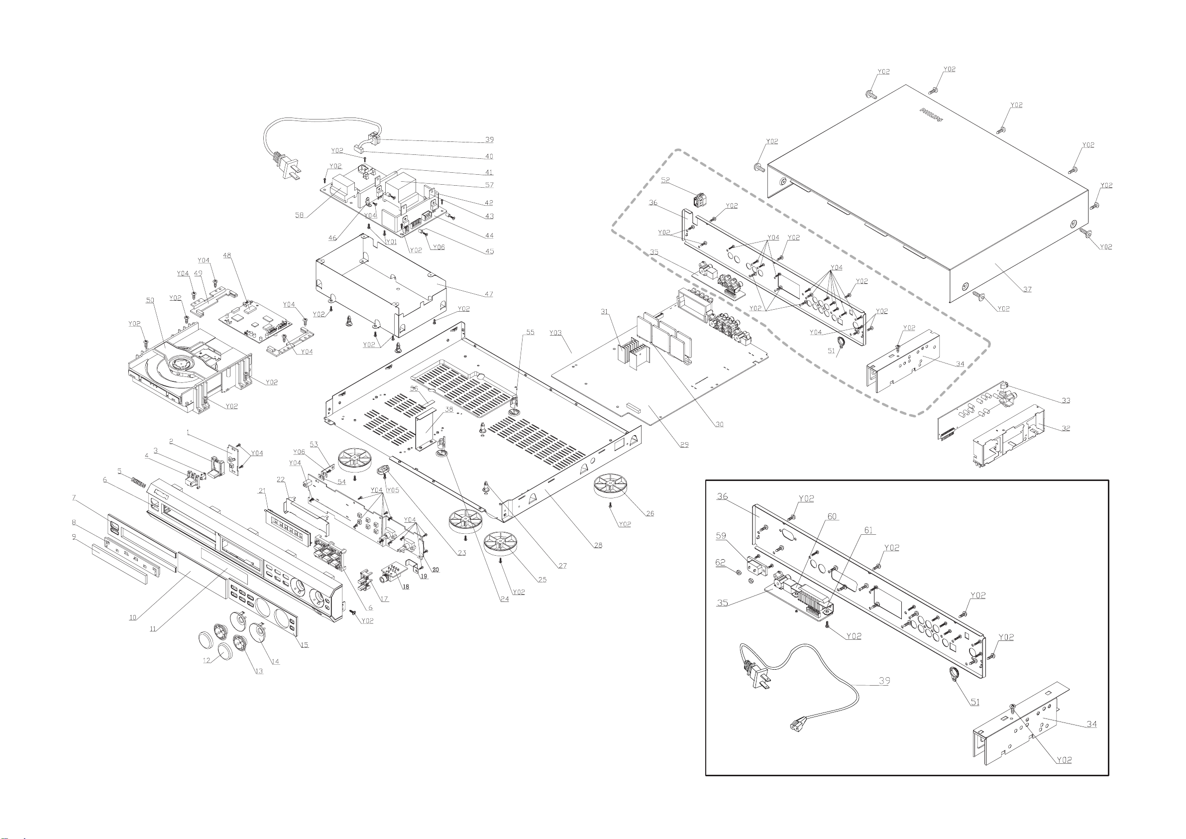
EXPLODED DRAWING
11-1
11-1
FOR MX3800 ONLY
Page 62

11-2
MECHANICAL & ACCESSORIES PARTS LIST - MAIN UINT SCREW LIST - MAIN UINT
11-2
2 9965 000 14096 OPEN / CLOSE KNOB
3 9965 000 14097 LED LENS
4 9965 000 14098 POWER KNOB
5 9965 000 12424 PHILIPS LOGO
6 9965 000 15477 FRONT PANEL MX3550D/37S
6 9965 000 14099 FRONT PANEL MX3600D/37
6 9965 000 14291 FRONT PANEL MX3700D/37S
6 9965 000 14216 FRONT PANEL MX3800D/21H/22S
7 9965 000 14217 POWER LENS /21H/22S
7 9965 000 14100 POWER KNOB TRIM /37
7 9965 000 14292 POWER LENS /37S
8 9965 000 14101 DVD DOOR
9 9965 000 14218 DOOR LENS /21H/22S
9 9965 000 14102 DOOR LENS /37/37S
10 9965 000 14219 VFD LENS /21H/22S
10 9965 000 14103 VFD LENS /37/37S
12 9965 000 14104 VOLUME CAB
13 9965 000 14105 VOLUME SHAFT
14 9965 000 14221 VOLUME RING
15 9965 000 14222 FUNCTION LENS /21H/22S
15 9965 000 14107 FUNCTION KNOB TRIM /37
15 9965 000 14293 FUNCTION LENS /37S
16 9965 000 14108 FUNCTION KNOB
17 9965 000 14109 BASS KNOB
24 9965 000 12437 PCB BRACKET
25 9965 000 14110 FOOT, SILVER
26 9965 000 14111 FOOT, BLACK
27 9965 000 12445 SPACER
39 9965 000 14112 BUSHING FIXED AC CORD
40 9965 000 15983!MAINS CORD /21H/22S
9965 000 14223 INSTRUCTION FOR USE MX3800D/22S
9965 000 14118 INSTRUCTION FOR USE MX3600D/37&
MX3700D/37S
9965 000 15478 INSTRUCTION FOR USE MX3550D/37S
9965 000 13060 REMOTE CONTROL
9965 000 13092 RGB CABLE 3P 1,5M except /22S
9965 000 13059 SCART CABLE 1M /22S
9965 000 14215 SATELLITE SPEAKER PACKAGE FOR
MX3800D/21H/22S
9965 000 14095 SATELLITE SPEAKER PACKAGE FOR
MX355D/37S & MX3600D/37
9965 000 14290 SATELLITE SPEAKER PACKAGE FOR
MX3700D/37S
9965 000 13057 RCA CABLE 1P 5M, SUBWOOFER
9965 000 14119 RCA CABLE 1P 1,2M VIDEO OUT
9965 000 14653 S-VIDEO CABLE
LOUDSPEAKER BOX BREAKDOWN
9965 000 14224 FRONT SPEAKER BOX /21H/22S
9965 000 14120 FRONT SPEAKER BOX /37/37S
9965 000 14225 SURROUND SPEAKER BOX /21H/22S
9965 000 14121 SURROUND SPEAKER BOX /37/37S
9965 000 14226 CENTER SPEAKER BOX /21H/22S
9965 000 14122 CENTER SPEAKER BOX /37/37S
9965 000 11846 GRILLE ASSY, FR/REAR SPK /37/37S
9965 000 11848 GRILLE ASSY, CENTER SPK /37/37S
9965 000 14123 MOUNTING BRACKET
Note: Only the parts mentioned in this list are normal service spare
parts.
Y01 M3 x 6
Y02 D3 x 6
Y03 D3 x 16
Y04 D3 x 8
Y05 D3 x 8
Y06 D3 x 10
40 9965 000 12818!MAINS CORD /37/37S
48 9965 000 13082 DVD FE SERVO PCB ASSY KIT572SE
48 9965 000 16291 DVD FE SERVO PCB ASSY KIT772SI
50 9965 000 12822 DVD LOADER MODULE KIT572SE
50 9965 000 15489 DVD LOADER MODULE KIT772SI
51 9965 000 12441 HOLDER
52 9965 000 12817 BUSHING /37/37S
55 9965 000 12455 PCB BRACKET
59 9965 000 12443
!
MAINS SOCKET /21H/22S
9965 000 14633 AM LOOP ANTENNA /21H
9965 000 14114 AM LOOP ANTENNA /22S/37/37S
9965 000 14115 FLEX CABLE 16PINS (CN201 TO DVD)
9965 000 14116 FLEX CABLE 26PINS (CN103 TO DVD)
9965 000 14117 FM ANTENNA
9965 000 16310 INSTRUCTION FOR USE MX3800D/21H
Page 63

12-1
DOCUMENT HISTORY
Version 1.0
* Initial release
Version 1.1
* New type/version MX3550D/37S has been added
Page 1-2 : Variation table adapted
Page 11-2 : Mechanical parts list adapted
* Correction / adaptation of Service Manual pages
Page 2-1 : Correction of type/version & add MX3550D/37S
Version 1.2
* The following pages are adapted to include new type/version MX3800D/21H:
Page 1-2, 1-3, 2-1, 5-5, 6-6, 8-10 to 8-12, 10-4 and 11-2
* Correction / adaptation of Service Manual pages
Page 7-2 to 7-6 : Improved circuit and layout diagrams (better readablity)
Page 7.7 : Correction of exploded view (pos 3)
Page 7-8 : Addition of service parts
Chapter 7A : Add DVD Module KIT771SI (including additional service parts)
Page 11-2 : correction for pos 14, 40 and add S-video cable
 Loading...