

Page 1

Micro System
MCM7000/12
egaPstnetnoC
1 Technical Specification and Connection Facilities
2 Laser Beam Safety Precautions......................................... 2-1
3 Important Safety Precautions .................................. 3-1 to 3-2
4 Safety Check After Servicing ............................................. 4-1
5 Safety Information General Notes & Lead Free
Requirements .................................................................... 5-1
6 Standard Notes For Servicing,Lead Free Requirements
& Handling Flat Pack IC .......................................... 6-1 to 6-4
7 Direction of Use ....................................................... 7-1 to 7-3
8 Cabinet Disassembly Instructions ........................... 8-1 to 8-2
9 Troubleshooting ....................................................... 9-1 to 9-2
10 Block Diagram .................................................................10-1
11 Wiring Diagram ...............................................................11-1
12 AMP Board
13 Display Board
©
Copyright 2011 Philips Consumer Electronics B.V. Eindhoven, The Netherlands.
All rights reserved. No part of this publication may be reproduced, stored in a
retrieval system or transmitted, in any form or by any means, electronic,
mechanical, photocopying, or otherwise without the prior permission of Philips.
Published by Sophie-KM 1114 AVM Printed in the Netherlands
Circuit Diagram ....................................................12-1
Layout Diagram ...................................................12-2
Circuit Diagram ................................................12-3
Layout Diagram ...............................................12-4
...................................................1-1 to 1-9
Contents
14 Headphone & MP3 Link and USB、LED Board
Circuit Diagram .................................................12-5
Layout Diagram.................................................12-5
15 Key Board
16 Power Board
17 Decoder Board
18 Exploded View....................................................................13-1
19 Revision List .......................................................................14-1
Circuit Diagram .................................................12-6
Layout Diagram ................................................12-7
Circuit Diagram ........................................12-8 to 12-9
Layout Diagram ..............................................12-10
Circuit Diagram .................................12-11 to 12-13
Layout Diagram ..............................................12-14
Feature
Features
RDS
Voltage Selector
ECO Standby
DTS
Subject to modi cation EN
Different
/12
Page
Version 1.0
Page 2

Location of PC Boards
DVD Loader
Key Board
USB Board
Technical Specification and Connection Facilities
Decoder Board
AMP Board
Power Board
Headphone/MP3 Link Board
Version Variations
Type /Versions:
Board in used:
LED Board
Decoder Board
Display Board
AMP Board
Headphone & MP3 Link Board
Power Board
USB Board
Key Board
Features
RDS
VOLTAGE SELECTOR
ECO STANDBY - DARK
DTS
* TIPS : C -- Component Lever Repair.
M -- Module Lever Repair
Service policy
Feature diffrence
-- Used
Display Board
Type /Versions
/05
/05
LED Board
/51
/12
C
M
C
C
C
M
C
C
/37
/12
/55
/55
/58
/58
MCM7000
/61
MCM7000
/61
/79
/79
/93
/93
/94
/94
/96
/96
/98
/98
1-1
Page 3
Technical Specification and Connection Facilities
Technical Specification
1. General Information and Requirement
1.1 Product Family Features
1.1.1 Identity and Key Features
MCM7000 series are Heritage Range Micro Audio System
CD/MP3 player with USB and Tuner FM(20presets)
Elements to include as generic requirements:
1. Detachable mains cord
2. Safety certification (cUL/FCC and CB/EMC/CE)
Following is a list of key features:
1. USB true source
a) MSC & MTP
b) USB High Speed
2. iPod/iPhone docking – Integrated, support iPad
3. MP3 Link (via headphones jack from PC or MP3 player)
4. Headphone Out (Front of the set TBC)
5. Tuner FM
6. Total output power
2x30Wrms
2.1.2 Styling, Forms and Functions
MCM7000 appearances are defined in their respective MUS. MUS is the leading document where product
appearance is applicable..
Features Products MCM7000
Stroke versions All
Design
Optical Drive Loading Tray
Front
Dimension
Weight With packaging 10kg
Cosmetics
Tray Orientation HORIZONTAL
ffothgieH
Main Unit
Speaker Box
W x D x H (mm)
roloC
snottuB
Refer to MUS[3] for
details
wolebnoitacoLyarT
PUDFV
mm3tee
250X92X285mm
174X260X240mm
Silver
Silver
1-2
Page 4
Technical Specification and Connection Facilities
2.1.3 External I/O Connections
Model
Stroke Version
USB
MP3 Link
(3.5mm audio jack)
Aux In
(RCA cinch)
Tuner Socket
(for FM)
Headphone Out
(3.5mm audio jack)
MCM7000
All
2.1.4 Controls, Local Display and LED Indications(tbc)
Control keys on the set are:
Model
Standby
Source(Disc/USB/FM/Aux/MP3_link)
MCM7000
Eject
Play/Pause
Volume Rotator
DSC
DBB
Treble Rotator
Bass Rotator
There is local display VFD. Standby LED colour:
N
N
N
N
Blue in Standby mode
1-3
Page 5

Technical Specification and Connection Facilities
2.1.5. ACCESSORIES (tbc)
Model MCM7000
Stroke Version 12
eporuEnoigeR
Power Cord
1.8M
AV cable 1.5M
Audio cable
(3.5mm audio)
Tuner Antenna
Speaker cable
USB cable
Remote Control
Battery
Quickly guide
IFU
0.5M
1.5M 75ohm
3M
NA
44keys
AAAx2
1
1
3.Mechanical General Information
The product
approves the MUS and it is a leading document where product appearance is applicable.
Please refer to Sh560 for mechanical information.
appearances and functions are defined in their respective MUS.Product management
3.1.Safety Standards
Where applicable:
For /12 (EU), /05 (UK), /51 (Russia) EN/IEC 60065 7th Edition
56006LU)adanaC,SU(73/roF
th
756006CEI)lizarB(87/,)MATAL(55/roF
Edition
For /98 (AP), /69 (Singapore), /75 (Australia) IEC 60065 7th Edition
th
006K)aeroK(16/roF
E
656
dition
756006CEI(8988BG)anihC(39/roF
6006CEI(80441SNC)nawiaT(69/roF
th
Edition)
th
75
3.2.EMC Requirements
Where applicable:
For /12 (EU), /05 (UK), /51 (Russia) EN55013: 2001, EN55020: 2002
51CCF)adanaC,SU(73/roF
31RPSIC)lizarB(87/,)MATAL(55/roF
For /98 (AP), /69 (Singapore), /75 (Australia) CISPR13
02/31RPSIC)aeroK(16/roF
C(39/roF
)31RPSIC(73831BG)anih
)31RPSIC(93431SNC)nawiaT(69/roF
Edition)
1-4
Page 6

Technical Specification and Connection Facilities
3.3.ESD Requirements
The product shall withstand electro static discharges on all user accessible parts of the product.
Reference: IEC61000-4-2.
For contact discharges:
Level
1
2 >2-4 >3-4
3 >4-5 >4-5
4 >5-7 >5-7
5 - >7-8
For air discharge:
Level
1 0-4 0-6
2 >4-8 >6-8
3 >8-10 >8-10
4 >10-15 >10-15
5 - >15-18 No loss of stored data allowed.
General(kV) USA(kV)
0-2 0-3
General(kV) USA(kV)
Requirement
No deviations allowed.
Short perceptible deviations allowed
Normal recallable functions functon changes allowed.
Control recallable functions function changes allowed.
No loss of stored data allowed.
Requirement
No deviations allowed.
Short perceptible deviations allowed
Normal recallable functions functon changes allowed.
Control recallable functions function changes allowed.
General requirement:
1. 10 arcs for positive and negative polarity for unit “on” and “off” for 1kV incremental steps.
2. Component or mechanical damage is not allowed. No loss of fixed stored data (stored in EEPROMs).
3. Hang-ups and malfunctions are allowed, as long as the customer can “recover” from the hang-up by
pressing the Standby or ON/OFF button of the set.
4. Failures that disappear only by unplugging the AC mains cord and/or power sources are not acceptable.
3.4.Environmental Condition
The environmental condition requirements and test method is according to UAN-D1590.
Ambient
temperature : max. 40 㷄 - all climates
Apparatus acc. to spec. : +5 to + 35㷄
Vibration test (acc. IEC 60 068/2/6) : operational vibration test to be proceeded in operating position of the
set.
3.5.Quality
PQR-class: class 2 according to BLC A&MA PQR handbook V2.1 (2006-10-02)
Lifetime: 7 years
Tested According to: General Test Instruction UAN-D 1591
Measured According to: UAN_L 1059 unless otherwise stated
1-5
Page 7
Technical Specification and Connection Facilities
4. Technical Specifications
Power Supply
4.1.1 Type and versions
Build-inSMPS will be used for all models and stroke versions.
All using figure '8' socket, will cater for all versions:
Versions Region/Country SMPS Detachable mains cords
05
/12
37
55
98
94
EUROPE/UK
NAFTA
LATAM
APAC
India
1) 100 ~240Vac nom. (wide
range from 90V~264Vac limit)
used in all versions except
India.
Frequency: 47~63Hz.
2) 100 ~310Vac limit (India
compatible with up cost) used
only for India.
Frequency: 47~63Hz.
EU(/12)round 2-pin & UK(/05) 3-pin
UL flat pin (non-polarized)
INMETRO certified round 2-pin
EU round 2-pin
EU (/12) round 2-pin
All requirements per defined for each country should be met with sufficient testing.
4.1.2 Surge Immunity (Lightning Test)
The product shall withstand mains interference’s of:
Differential mode:
2kV/2 ohm criteria C for Europe.
6kV/12 ohm criteria C for NAFTA.
Parameters:
Bi-wave
Open circuit voltage: 2/50us
Short circuit current: 8/20us
From +/1kV to +/-2kV (for Europe) or +/-6kV (for Nafta) in steps of 1kV.
10 shots per combination.
One shot per minute.
Serial impedance: 2 Ohm for Europe, 12Ohm for Nafta.
Polarity and phase: Positive (phase 90º) & Negative (phase 270º)
Common mode:
6kV/2 ohm criteria C for Europe.
6kV/12 ohm criteria C for Nafta.
Parameters:
Ring-wave (100kHz)
From +/3kV to +/-6kV in steps of 1 kV.
10 shots per combination.
One shot per minute.
Serial impedance: 2 Ohm for Europe, 12Ohm for Nafta
Polarity and phase: Positive (phase 90º) & Negative (phase 270º)
Reference: IEC61000-4-5 and for USA: 3135 019 8029 Reliability evaluation.
Requirements:
Apparatus should fulfil the leakage current requirements of IEC60065 point 9.1.1 (UAN-D1631)
Defects or permanent deviations are not allowed.
1-6
Page 8

Technical Specification and Connection Facilities
4.1.3 Mains Drop-out Immunity
The product shall withstand mains failures of:
Variation 0% (=100% dip) at T-event = 50 mSec. Performance criterion B
Variation 40% (=60% dip) at T-event = 100 mSec. Performance criterion B
Variation 0% (=100% dip) at T-event = 5 Sec. Performance criterion C
Additional for USA apparatus: See 3135 019 8029 Reliability evaluation.
Variation 0% (=100% dip) at T-event = 100 mSec in standby mode. Performance criterion B
Requirement:
No misoperation and no interference of user in order to guarantee continuation of performed function.
Reference: IEC61000-4-11 For measuring method refer to UAN-D1724, as far as applicable.
Performance criterions according to IEC61000-4-4 Amendment 1
Performance Requirement
Criterion A - No any degradation of specification.
Criterion B - Temporary degradation / self recoverable.
Criterion C - No damage, resolvable hang-up.
Criterion D - Not recoverable loss of function.
4.1.4 Power Consumption
Power consumption at nominal AC input:
1. CD play mode at 1/8 P-rated output power MCM7000: 40
2. Low Power Standby Mode :
0.5
W
W
1-7
Page 9

Technical Specification and Connection Facilities
traPlarenreG
Output Stage Protection: NA Temperature : Yes Short Circuit: Yes
srotacidnI
evitcAyalpsiDkcolC:rotacidnIedoMybdnatS
ffOsnruTDEL:edoMybdnatSrewoP
Electrical Data
±
3dB
loV(muHAN:BBD
min
--- Vol
:ecnereffiDlennahCAN:CSD
-20dB) 150nW
max
Wn04)muminiMemuloV(esioNlaudiseRY:ssaB
Bd53/Bd04zHk01/zHk1:noitarepeSlennahCY:elberT
%8.0<lamixaM,DHTY:ssenduoL
Signal to Noise Ratio(A-weighted):
:klatssorC
82dB
55dB
Audio Inputputs
Audio Input Sensitivity( 3dB) rated output power at 1kHz
±
Audio Output(*1)
Tuner FM 67.5kHz, Modulation (Limit:-6dB) Line Out(Left/Right) NA
CD/MP3 0dB track (Audio Disc 1, Track 1) Headphone 15mW ± 2 dB, RL = 32
)SH0.2(evaweniszHK1Bd0BSU
AUX1(back)
MP3_link(front)
IPOD Docking
1000mV 100mV; Rin 22k
500mV 100mV; Rin 22k
800mV 100mV Rin 22k
±
±
±
Output Power(*1) At THD=10%, 1kHz sinewave MCM7000
Main Operation for / all version (rms)
Tuner output power(rms)
Frequency Response( 3dB)
±
±
30W 1dB
±
30W 1dB
30Hz-20kHZ
( At Cold Condition with 10% THD )
( At Cold Condition with 10% THD )
Loudspeaker(Boxes): Separable speaker box Refer to package document of Speaker Box Assy
Speaker driver Impedance: Right/Left: 4 30 Hz ~ 20kHz(-3db)
:refoowbuS
REMARKS:
Electrical Parameters are to be measured at Speaker Terminals across rated impedance Load(6ohm) with
Rated Input Signal in CD Mode setting in DBB/Loudness Off and Pre-eq at Flat unless specified otherwise.
1-8
Page 10

Technical Specification and Connection Facilities
5.TUNER
FM use Silicon Lab Si4704/4705(w/RDS)
GENARAL PART
WAVE RANGE VERSION TOLERANCE TUNING GRID
FM 87.5 – 108.00 MHz /05/12 QUARTZ PRECISION 50kHz
AERIAL
FM : PIG TAIL ANT WIR(ȍ
ELECTRICAL DATA
)edomoeretsta(ytivitisneSgninuThcraeS3541
Search time digital tuning
system.
Overall Frequency Response: 63Hz –
12.5KHz
Channel separation:400 / 1000 / 5000 Hz.
Frequency (MHz)
FM Nom. 18 30 64 1000 22
88.0 Lim. 22 25 45 500 18 (*1)
FM Nom. 18 30 64 1000 22
98.0 Lim. 22 25 45 500 18 (*1)
FM Nom. 18 30 60 116 dBf 45
107.0 Lim. 22 25 65 108 dBf 25
Units dBf DB dB mV/m dB
Noise Limited
Sensitivity 26 dB
RF input: 68 dBf
Image
Rejection
IF Rejection
Large Signal
Handling
-60S
-±3dB
26/30/2020/26/
Selectivity
S9/300 kHz
tinUtimiLmoNMF
fBd6202tnioPgnitimiLBd3-
zHM7.01FI
5405muHnoitaludoM
5405oitaRN/S
18
Bd1584gniteiuQBd64-oeretS
Bd4-0esreveRnoitacifilpmA
%32)zHk57.veDqrF,Vm1FR(noitrotsiD
dB
Susceptibility to unwanted signals(CPU,SMPS,AMP,DSP …):
Limited(dB)Normal
-15dB -20dB Refer to selfpollution curve
(dB)
Remark
1-9
Page 11
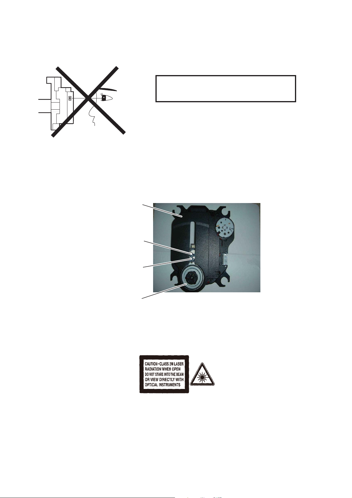
Laser Beam Safety Precautions
This Blu-Ray player uses a pickup that emits a laser beam.
Do not look directly at the laser beam coming
from the pickup or allow it to strike against your
skin.
The laser beam is emitted from the location shown in the figure. When checking the laser diode, be sure to keep
your eyes at least 30 cm away from the pickup lens when the diode is turned on. Do not look directly at the laser
beam.
CAUTION: Use of controls and adjustments, or doing procedures other than those specified herein, may result in
hazardous radiation exposure.
Drive Mechanism Assembly
Laser Beam Radiation
Laser Pickup
Turntable
Location: Inside Top of Blu-Ray mechanism.
2-1
Page 12

Important Safety Precautions
Important
Read and understand all instructions before you use
your home theater. If damage is caused by failure to
follow instructions, the warranty does not apply.
Safety
Riskof electricshock or fire!
Neverexposetheproductand
accessories to rain or water. Never place
liquid containers, such as vases, near the
product. If liquids are spilt on or into the
product, disconnect it from the power
outlet immediately. Contact Philips
Consumer Care to have the product
checked before use.
Never place the product and accessories
near naked
including direct sunlight.
Never insert objects into the ventilation
slots
or other openings on the product.
Where the mains plug or an appliance
coupler is used as the disconnect device,
the disconnect device shall remain readily
operable.
Disconnect the product from the power
outlet before lightning storms.
When you disconnect the power cord,
always pull the plug, never the cable.
Riskof short circuit or
Before you connect the product to the
poweroutlet,ensurethatthepower
voltage matches the value printed on the
back or bottom of the product. Never
connec
if the voltage is different.
Risk of injury or damage to the home theater!
For wall-mountable products, use only
the supplied wall mount bracket. Secure
the wall mount to a wall that can support
the combined weight of the product
and the wall mount. Koninklijke Philips
Electronics N.V. bears no responsibility
for improper wall mounting that results in
accident,injuryordamage.
ames or other heat sources,
re!
ttheproducttothepoweroutlet
For speakers with stands, use only the
supplied stands. Secure the stands to
the speakers tightly. Place the assembled
stands on flat, level surfaces that can
support the combined weight of the
speaker and stand.
Never place the product or any objects
on power cords or on other electrical
equipment.
If the product is transported in
temperatures below 5°C, unpack the
product and wait u
matches room temperature before
connecting it to the power outlet.
Visible and invisible la
open. Avoid exposure to beam.
Do not touch the disc optical lens inside
the disc compartment.
Risk of overheating!
Never install this product in a confined
space. Always leave a space of at least
four inches around the product for
ventilation. Ensure curtains or other
objects never cover the ventilation slots
on the product.
Risk of contamination!
Do not mix batteries (old and new or
carbon and alkaline,
Remove batteries if they are exhausted
or if the remote control is not to be used
for a long time.
Batteries contain chemical substances,
they should be disposed of properly.
ntil its temperature
ser radiation when
etc.).
Product care
Do not insert any objects other than discs
into the disc compartment.
Do not insert warped or cracked discs
into the disc compartment.
Remove discs from the disc compartment
ifyouarenotusingtheproductforan
extended period of time.
Only use microfiber cloth to clean the
product.
3-1
Page 13

Important Safety Precautions
Disposal of your old product and
batteries
Your product is designed and manufactured
with high quality materials and components,
which can be recycled and reused.
When this crossed-out wheeled bin symbol
is attached to a product it means that the
product is covered by the European Directive
2002/96/EC.Pleaseinformyourselfaboutthe
local separate collection system for electrical
and electronic products.
Please act according to your local rules and
do not dispose of your old products with your
normal household waste.
Corr
ect disposal of your old product helps to
prevent potential negative consequences for
the environment and human hea
lth.
Your product contains batteries covered by
the European Directive 2006/66/EC, which
cannot be disposed with normal household
waste.
Please inform yourself about the local rules
on separate collection of batteries because
correct disposal helps to prevent negative
consequences for the environmental and
human health.
3-2
Page 14

Safety Check after Servicing
Examine the area surrounding the repaired location for damage or deterioration. Observe that screws, parts, and
wires have been returned to their original positions. Afterwards, do the following tests and confirm the specified
values to verify compliance with safety standards.
1. Clearance Distance
When replacing primary circuit components, confirm
specified clearance distance (d) and (d’) between
soldered terminals, and between term
surrounding metallic parts. (See Fig. 1)
Table 1: Ratings for selected area
inals and
Chassis or Secondary Conductor
Primary Circuit
AC Line Voltage Clearance Distance (d), (d
110V~220V
Note
: This table is unofficial and for reference only. Be
sure to confirm the precise values.
3.2 mm (0.126 inches)
’)
2. Leakage Current Test
Confirm the specified (or lower) leakage current
between B (earth ground, power cord plug prongs) and
externally exposed accessible parts (RF terminals,
antenna terminals, video and audio input and output
terminals, microphone jacks, earphone jacks, etc.) is
than or equal to the specified value in the table
lower
below.
Measuring Method (Power ON):
Insert load Z between B (earth ground, power cord plug
prongs) and exposed accessible parts. Use an AC
eter to measure across the terminals of load Z.
voltm
See Fig. 2 and the following table.
d' d
Fig. 1
Exposed Accessible Part
Z
AC Voltmeter
(High Impedance)
Earth Ground
B
Power Cord Plug Prongs
Table 2: Leakage current ratings for selected areas
AC Line Voltage Load Z Leakage Current (i) Earth Ground (B) to:
110V~220V
Note: This table is unofficial and for reference only. Be sure to confirm the precise values.
0.15 μF CAP. & 1.5 k
Connected in parallel
RES.
i
0.5 mA Peak Exposed accessible parts
4-1
Fig. 2
Page 15

Safety Information, General Notes & Lead Free Requirements
1 Safety Instructions
1.1 General Safety
Safety regulations require that during a repair:
Connect the unit to the mains via an isolation transformer.
Replace safety components, indicated by the symbol
only by components identical to the original ones. Any
other component substitution (other than original type)
Safety regulations require that after a repair, you must return
the unit in its original condition. Pay, in particular, attention to
the following points:
Route the wires/cables correctly
mounted cable clamps.
damage.
Check the electrical DC resistance between the mains
plug and the secondary side:
1. Unplug the mains cord, and connect a wire between
the two pins of the mains plug.
2. Set the mains switch to the ‘on’ position (keep the
mains cord unplugged!).
3. Measure the resistance value between the mains
plug and the front panel, controls, and chassis
bottom.
4. Repair or correct unit when the resistance
5. Verify this, before you return the unit to the customer/
user (ref. UL-standard no. 1492).
6. Switch the unit ‘off’, and remove the wire between the
two pins of the mains plug.
1.2 Laser Safety
This unit employs a laser
may remove the cover, or attempt to service this device (due
to possible eye injury).
2 Warnings
2.1 General
All ICs and many other semiconductors are susceptible to
,
during repair can reduce life drastically. Make sure that,
during repair, you are at the same potential as the mass
of the set by a wristband with resistance. Keep
components and tools at this same potential.
Available ESD protection equipment:
– Complete kit ESD3 (small tablemat, wristband,
4822 310 10671.
– Wristband tester 4822 344 13999.
Be careful during measurements in the live voltage
section. The primary side of the power supply, including
the heatsink, carries live mains voltage when you
connect the player to the mains (even when the
player is ‘off’!). It is possible to touch copper tracks and/
or components in this unshielded primary area, when
you service the player. Service personnel must take
precautions to prevent touching this area or components
in this area. A ‘lightning stroke’ and a stripe-marked
printing on the printed wiring board, indicate the primary
side of the power supply.
Never replace modules, or components, while the unit is
‘on’.
2.2 Laser
The use of optical instruments with this product, will
Only quali ed service personnel may remove the cover or
attempt to service this device, due to possible eye injury.
Repair handling should take place as much as possible
with a disc loaded inside the player.
T
shield:
electrostatic discharges (ESD,
). Careless handling
Laser Device Unit
epyT
:AIGalnN(BD)
:AIGalnP(DVD)
: AIGalnP(CD)
Wavelength : 650 nm (DVD)
)DC/DCV(mn087:
405nm(BD):
Output Power : 20 mW
)gnitirwWR+DVD(
Wm8.0:
)gnidaerDVD(
Wm3.0:
)gnidaerDC/DCV(
Beam divergence : 60 degree
CLASS 1
LASER PRODUCT
1-2erugiF
Note: Use of controls or adjustments or performance of
procedure other than those speci
ed herein, may result in
A
CAUTION VISIBLE AND INVISIBLE LASER RADIATION WHEN OPENAVOID EXPOSURE TO BEAM
ADVARSEL SYNLIG OG USYNLIG LASERSTRÅLING VED ÅBNING UNDGÅ UDSÆTTELSE FOR STRÅLING
ADVARSEL SYNLIG OG USYNLIG LASERSTRÅLING NÅR DEKSEL ÅPNES UNNGÅ EKSPONERING FOR STRÅLEN
VARNING SYNLIG OCH OSYNLIG LASERSTRÅLNING NÄR DENNA DEL ÄR ÖPPNAD BETRAKTA EJ STRÅLEN
VARO!AVATTAESSA OLET ALTTIINA NÄKYVÄLLE JA NÄKYMÄTTÖMÄLLE LASER SÄTEILYLLE. ÄLÄ KATSO SÄTEESEEN
VORSICHT SICHTBARE UND UNSICHTBARE LASERSTRAHLUNG WENNABDECKUNG GEÖFFNET NICHT DEM STRAHL AUSSETSEN
DANGER VISIBLE AND INVISIBLE LASER RADIATION WHEN OPENAVOID DIRECT EXPOSURE TO BEAM
ATTENTION RAYONNEMENT LASER VISIBLE ET INVISIBLE EN CAS D’OUVERTURE EXPOSITION DANGEREUSE AU FAISCEAU
Figure 2-2
5-1
Page 16

Standard Notes for Servicing, Lead Free Requirements & Handling Flat Pack IC
Circuit Board Indications
1. The output pin of the 3 pin Regulator ICs is
indicated as shown.
Top View
Out
2. For other ICs, pin 1 and every fifth pin are
indicated as shown.
Pin 1
3. The 1st pin of every male connector is indicated as
shown.
Pin 1
Input
In
Bottom View
5
10
Instructions for Connectors
1. When you connect or disconnect the FFC (Flexible
Foil Connector) cable, be sure to first disconnect
the AC cord.
2. FFC (Flexible Foil Connector) cable should be
inserted parallel into the connector, not at an
angle.
FFC Cable
Connector
CBA
* Be careful to avoid a short circuit.
Pb (Lead) Free Solder
When soldering, be sure to use the Pb free solder.
Information about lead-free soldering
Philips CE is producing lead-free sets from 1.1.2005
onwards.
IDENTIFICATION
Regardless of special logo (not always
indicated)
One must treat all sets from
onwards, according to the next rule:
Serial Number gives a 14-digit. Digit 5&6 shows the
YEAR, and digit 7&8 shows the WEEK.
So from onwards=from 1 Jan 2005 onwards
0501
Important note : In fact also products of year 2004
must be treated in this way as long as you avoid
mixing solder-alloys (leaded/ lead-free). So best to
always use SAC305 and the higher temperatures
belong to this.
Due to lead-free technology some rules have to be
respected by the workshop during a repair:
Use only lead-free solder alloy Philips SAC305 with
order code 0622 149 00106. If lead-free solderpaste is required, please contact the manufacturer
of your sol
paste within workshops should be avoided because
paste is not easy to store and to handle.
Use only adequate solder tools applicable for leadfree solder alloy. The solder tool must be able
To reach at least a solder-temperature of 400°C,
To stabilize the adjusted temperature at the solder-
tip
To exchange solder-tips for different applications.
Adjust your solder tool so that a temperature around
360°C
solder joint. Heating-time of the solder-joint should
not exceed ~ 4 sec. Avoid temperatures above
400°C otherwise wear-out of tips will rise drastically
and flux-fluid will be destroyed. To avoid wear-out of
tips switch off un-used equipment, or reduce heat.
Mix of lead-free solder alloy / parts with leaded
solder alloy / parts is possible but PHILIPS
recommends strongly to avoid mixed solder alloy
types (leaded
If one cannot avoid or does not know whether
product is lead-free, clean carefully the solder-joint
from old solder alloy and re-solder with new solder
alloy (SAC305).
Use only original spare-parts listed in the ServiceManuals. Not listed standard-material (commodities)
has to be purchased at external companies.
der-equipment. In general use of solder-
- 380°C is reached and stabilized at the
and lead-free).
1 Jan 2005
6-1
Page 17
Standard Notes for Servicing, Lead Free Requirements & Handling Flat Pack IC
Special information for BGA-ICs:
- always use the 12nc-recognizable soldering
temperature profile of the specific BGA (for desoldering always use the lead-free temperature
profile, in case of doubt)
- lead free BGA-ICs will be delivered in so-called
'dry-packaging' (sealed pack including a silica gel
pack) to protect the IC against moisture. After
opening, dependent of MSL-level seen on indicatorlabel in the bag, the BGA-IC possibly still has to be
baked dry. (MSL=Moisture Sensit
will be communicated via AYS-website.
Donotre-useBGAsatall.
For sets produced before 1.1.2005 (except products
of 2004), containing leaded solder-alloy and
components, all needed spare-parts will be available
till the end of the service-period. For repair of such
sets nothing changes.
On our website
www.atyourservice.ce.Philips.com
information to:
BGA-de-/soldering (+ baking instructions)
Heating-profiles of BGAs and other ICs used in
Philips-sets
You will find this and more technical information within
the “magazine”, chapter “workshop news”.
For additional questions please contact your local
repair-helpdesk.
ivity Level). This
you find more
How to Remove / Install Flat Pack-IC
1. Removal
With Hot-Air Flat Pack-IC Desoldering Machine:
1. Prepare the hot-air flat pack-IC desoldering
machine, then apply hot air to the Flat Pack-IC
(about 5 to 6 seconds). (Fig. S-1-1)
Fig. S-1-1
2. Remove the flat pack-IC with tweezers while
applying the hot air.
3. Bottom of the flat pack-IC is fixed with glue to the
CBA; when removing entire flat pack-IC, first
soldering iron to center of the flat pack-IC and heat
up. Then remove (glue will be melted). (Fig. S-1-6)
4. Release the flat pack-IC from the CBA using
tweezers. (Fig. S-1-6)
apply
CAUTION:
1. The Flat Pack-IC shape may differ by models. Use
an appr
machine, whose shape matches that of the Flat
Pack-IC.
2. Do not supply hot air to the chip parts around the
flat pack-IC for over 6 seconds because damage
to the chip parts may occur. Put masking tape
around the flat pack-IC to protect other parts from
damage. (Fig. S-1-2)
opriate hot-air flat pack-IC desoldering
6-2
Page 18

Standard Notes for Servicing, Lead Free Requirements & Handling Flat Pack IC
3. The flat pack-IC on the CBA is affixed with glue, so
be careful not to break or damage the foil of each
pin or the solder lands under the IC when
removing it.
Hot-air
Flat Pack-IC
Desoldering
CBA
Masking
Tape
Machine
Flat Pack-IC
Tweezers
Fig. S-1-2
With Soldering Iron:
1. Using desoldering braid, remove the solder from
all pins of the flat pack-IC. When you use solder
flux which is applied to all pins of the flat pack-IC,
you can remove it easily. (Fig. S-1-3)
Flat Pack-IC
Desoldering Braid
4. Release the flat pack-IC from the CBA using
tweezers. (Fig. S-1-6)
With Iron Wire:
1. Using desoldering braid, remove
all pins of the flat pack-IC. When you use solder
flux which is applied to all pins of the flat pack-IC,
you can remove it easily. (Fig. S-1-3)
2. Affix the wire to a workbench or solid mounting
point, as shown in Fig. S-1-5.
3. While heating the pins using a fi
iron or hot air blower, pull up the wire as the solder
melts so as to lift the IC leads from the CBA
contact pads as shown in Fig. S-1-5.
4. Bottom of the
CBA; when removing entire flat pack-IC, first apply
soldering iron to center of the flat pack-IC and heat
up. Then remove (glue will be melted). (Fig. S-1-6)
5. Release the flat pack-IC from the CBA using
tweezers. (Fig. S-1-6)
Note: When using a soldering iron, care must be
taken to
being held by glue. When the flat pack-IC is
removed from the CBA, handle it
because it may be dama
flat pack-IC is fixed with glue to the
ensure that the flat pack-IC is not
the solder from
ne tip soldering
gently
ged if force is applied.
Hot Air Blower
Soldering Iron
Fig. S-1-3
2. Lift each lead of the flat pack-IC upward one by
one, using a sharp pin or wire to whic
not adhere (iron wire). When heating the pins, use
a fine tip soldering iron or a hot air de
machine. (Fig. S-1-4)
h solder will
soldering
Sharp
Pin
Fine Tip
Soldering Iron
3. Bottom of the flat pa
CBA; when removing entire flat pack-IC, first apply
soldering iron to center of the flat pack-IC and heat
up. Then remove (glue will be melted). (Fig. S-1-6)
ck-IC is fixed with glue to the
Fig. S-1-4
6-3
To Solid
Mounting Point
CBA
Tweezers
or
Iron Wire
Soldering Iron
Fig. S-1-5
Fine Tip
Soldering Iron
Flat Pack-IC
Fig. S-1-6
Page 19

Standard Notes for Servicing, Lead Free Requirements & Handling Flat Pack IC
2. Installation
1. Using desoldering braid, remove the solder from
the foil of each pin of the flat pack-IC on the CBA
so you can install a replacement flat pack-IC more
easily.
2. The “
(See Fig. S-1-7.) Be sure this mark matches the 1
on the PCB when positioning for installation. Then
presolder the four corners of the flat pack-IC. (See
Fig. S-1-8.)
3. Solder all pins of the flat pack-IC. Be sure that
none of the pins have solder bridges.
” mark on the flat pack-IC indicates pin 1.
Example :
Pin 1 of the Flat Pack-IC
is indicated by a " " mark.
Fig. S-1-7
Instructions for Handling Semiconductors
Electrostatic breakdown of the semi-conductors may
occur due to a potential difference caused by
electrostatic charge during unpacking or repair work.
1. Ground for Human Body
Be sure to wear a grounding band (1 M ) that is
properly grounded to remove any static electricity that
may be charged on the body.
2. Ground for Workbench
Be sure to place a conductive sheet or copper plate
with proper grounding (1 M
other surface, where the semi-conductors are to be
placed. Because the static electricity charge on
clothing will not escape through the body grounding
band, be
with your clothing.
careful to avoid contacting semi-conductors
<Incorrect>
) on the workbench or
CBA
Presolder
Flat Pack-IC
Fig. S-1-8
<Correct>
1M
CBA
Grounding Band
1M
CBA
Conductive Sheet or
Copper Plate
6-4
Page 20

Direction of Use
*The following excerpt of the DFU/QSG serves as an introduction to the set.
The Complete Direction for Use can be download in different languages from
the internet site of Philips Customer care Center : www.support.philips.com
Overview of the main unit
SOURCE
3
1
14
13
1
2
12
Switch to ECO Power or standby
mode.
2
SOURCE
Select a source.
3
/
Skip to the previous/next track.
Skip to the previous/next title or chapter.
Tune to a radio station.
4
Start or pause play.
/
5
Search backward or forward.
Search to a radio station.
6
Stop play.
Erase a program.
(In standby mode) Turn on/off Demo
mode.
7
Open or close the disc
compartment.
8
VOLUME
Adjust volume.
Adjust time.
9
IR sensor
Detect signals from the remote
control. Always point the remote
controlattheIRsensor.
10
Display panel
Display information about current
source.
11
Disc compartment
Hold the disc.
4
11
Overview of the main unit
12
Headphone socket.
13
MP3 LINK
Connect to an external audio device.
14
5
6
10
9
7
Connect to aUSB Àash drive.
Overview of Remote control
1
23
22
8
21
20
19
18
17
16
15
14
1
Switch to ECO Power or standby
mode.
2
DIM
Adjust brightness of display panel.
(Press and hold) Turn on or off the
LEDlightatthebottom of theunit
andatthevolumeknob.
2
3
4
5
6
7
8
9
10
11
12
13
7-1
Page 21

Direction of Use
Remote control
3
SHUFFLE
Play tracks randomly.
4
SLEEP
Set the sleep timer.
5
Navigate through menu.
ALBUM/
album; skip to a preset station.
OK
Con¿rmanentryor selection.
Select FM stereo or mono.
6
RDS/INFO
ForselectedFMradiostations:
display RDS information.
Displaythecurrentstatusorthedisc
information.
Display the ID3 information
(if available) of MP3 tracks.
7
/
Skiptothepreviousornexttitle,
chapter, track, or radio station.
8
Stop play.
Erase a program.
(In standby mode) Turn on/off Demo
mode.
9
/
search backwards or forward.
Search to a radio station.
10
TREBLE / BASS
Activate treble/bass adjustment.
11
CLOCK
Set the clock.
Display the set clock.
12
Numeric keypad.
Select a track directly.
13
SHIFT
Enter a two or three-digit number
(withthenumerickeypad).
14
PROGRAM
Program radio stations.
Program tracks.
15
VOL +/-
Adjust volume.
Adjust time.
16
LOUDNESS
Turn on or off automatic loudness
adjustment.
17
Mute or restore volume.
18
Start or pause play.
:Skiptoprevious/next
19
MENU
Access menu.
This button is not workable for this
model.
20
TIMER
Set alarm timer.
21
Open or close the disc
compartment.
22
REPEAT
Select a repeat play mode.
23
Source buttons
Select a source.
DOCK source is not available for this
unit.
3 Get started
Caution
Useofcontrolsoradjustmentsor
performanceofproceduresotherthanherein
mayresultinhazardousradiationexposureor
other unsafe operation.
Always follow the instructions in this chapter in
sequence.
If you contact Philips, you will be asked for the
model and serial number of this apparatus.The
model number and serial number are on the
back of the apparatus.Write the numbers here:
Model No. __________________________
Serial No. ___________________________
Connect speakers
Note
Ensure that the colors of the speaker wires and
terminals are matched.
For optimal sound, use the supplied speakers
only.
Connectonlyspeakerswithimpedancethatis
the same or higher than the supplied speakers.
Referto theSpeci¿cations section of this
manual.
For the main unit side:
Connect the speaker wires and the main unit as
the following graphic indicates:
7-2
Page 22

For the speaker side:
1 Unscrew the speaker connectors.
2 For the left speaker, identify the speaker
cable that is connected to the left
connectors on the main unit.
3 Insertfullytheredend of thespeaker
cable into the red (+) connector.
4 Screwthered(+)connectortosecure
the cable.
5 Insert fully the silver end of the speaker
cable into the black (-) connector.
6 Screw the black (-) connector to secure
the cable.
7 Repeat steps 2-6 for the right speaker.
Connect FM antenna
Direction of Use
1 Connectthepowercordto:
LL
FM
RR
DEMO
ANTENNA
AUXINLINEOUT
the AC~socketonthemainunit.
the power outlet.
LL
FM
RR
DEMO
ANTENNA
AUXINLINEOUT
FM
Tip
Foroptimalreception,fullyextendandadjust
thepositionoftheantenna.
ForbetterFMstereoreception,connectan
outdoorFMantennatothe FMANTENNA
socket.
TheunitdoesnotsupportMWradio
reception.
1 Connect the supplied FM antenna to the
FMANTENNAsocketonthemainunit.
Connect power
Caution
Risk of product damage! Ensure that the
power supply voltage corresponds to the
voltageprintedonthebackortheunderside
of the unit.
Risk of electric shock! When you unplug the
AC power cord, always pull the plug from the
socket.Neverpullthepowercord.
Before you connect the AC power cord,
ensurethatyouhavecompletedallother
connections.
7-3
Page 23

Cabinet Disassembly Instructions
1. Disassembly Flowchart
This flowchart indicates the disassembly steps to gain
access to item(s) to be serviced. When reassembling,
follow the steps in reverse order. Bend, route, and
dress the cables as they were originally.
[1].Top CAB
[2].Decoder Board
[3].Back CAB/AC Socket
[4].AMP Board
[5].Power Board
[6].Decoration Plates
[7].Front CAB
[8].DVD Loader Bracket/
DVD Loader
2. Disassembly Method
Note:
(1) Identification (location) No. of parts in the figures
(2) Name of the part
(3) Figure Number for reference
(4) Identification of parts to be removed, unhooked,
unlocked, released, unplugged, unclamped, or
desoldered.
Axx = Screw
, CNxx/Jxx/CONxx = Connector
D3.5X12BA is specification of screw.
* = Unhook, Unlock, Release, Unplug, or Desolder
e.g. 7(A01) = seven Screws
A01
A01
ID/Loc.
NO.
[1] Top CAB
[2] Decoder Board
[3]
[4]
[5]
[6]
[7]
[8]
Part
Back CAB
AC Socket
AMP Board
Power Board
Decoration
Plates
Front CAB
DVD Loader
Bracket/DVD
Loader
Fig.NO.
D1
D2
D3
D4
D5
D6
D7
D8
Removal
Remove/Unhook
/Unlock/Release/
Unplug/Desolder
7(A01) D3*12 BA
2(A02)D3X8 PA
3(A03)D3X8 BA
5 (A04) D3X5 PMTT
1 (A05) D3X8 BA
2 (A06) D3X8 PA
1 (A07) D3X8 BM
1 (A08) D3X5 PMTT
1 (A09) D3X8 BA
2 (A10) D3X8 FA
4 (A011) D3X5 PM
4 (A012) D3X12 BA
Note
Fig. D1
A03
A02
Fig. D2
8-1
Page 24

A06
Cabinet Disassembly Instructions
A04
A05
Fig. D3
Fig. D4
A04
A010
A04
Fig. D6
A07
A08
Fig. D7
Fig. D5
A09
A011
A012
Fig. D8
8-2
Page 25

FLOW CHART NO.1
NO Power(The power cannot be turned on)
Troubleshooting
Check the Power Cable connect is ok or not
Yes
TEST Power supply voltage output CON4 each
plate is normal or not(+12V\DC5V\MCU\5V\P25V)
Yes
Check & replace AMP&MCU BOARD
FLOW CHART NO.2
No
No
Check and Change the connect cable
TEST CON4 “ECO”pin whether
has high level signal
No
Check the fuse which location F1
is normal or not.
Replace the power board
Yes
Yes
No
replace a new one
Has not voice form the speaker
Adjust the Volume
Ye s
Check speakers boxes are connected correctly
Ye s
Check if the operate system in MUTE state
Ye s
Check&replace AMP&MCU board
Yes
No
Retry again
Cancel the MUTE setup
9-1
Page 26

FLOW CHART NO.3
VFD no display
Check VFD display board CN301 whether connection to decoder
board CN1 is normal
Ye s
Troubleshooting
Test whether VFD board CN401 pin 12#~13# between
has AC5V provide voltage
Ye s
Check whether VFD board U401 pin 14#\33#\45# has +V5
supply voltage,and the pin 34# whether has -27V supply voltage
Ye s
Check pin #9,#10,#11(STB,CLK,DATA)of CN401 in VFD
board to see the signal is normal or not.
Ye s
Check&replace a new U401(PT6311)
FLOW CHART NO.4
Pass in and out can not read dish sometime.
No
Check VFD display board CN401 whether
connection to KEYS board CN301 is normal
No
Check the KEYS board location
B301 related electric circuit
No
Check&replace MCU board
Check dish if put on the right position or not.
Yes
Check dish if cleanlily or not.
Yes
Check & replace a new driver loader .
9-2
Page 27

Block Diagram
SONY pick up
DM-06BXLX-L2
DVD Loader
USB
USB
5V 1A
M5V
Loader motor drive r
CD5888CB(1.18V)
23.7K 1% resistor
Power Switch
TPS2552DBVT
ESD REJECTOR
MAIN BOARD
EN0
OC0
USB2 FRONT
DVD AUDIO IIS
M3.3V
Main chipset
ZR36966XE2
AMUTE
DVD IIC
DVD ON
DVD RST
M1.8V
CN?
12V /1A (11.7V-12.3V)
6
GND
5
28V 6A
4
28V 6A
3
GND
2
GND
M3.3V
SDRAM
M12L64164A-7T
M3.3V
FLASH
2M * 8 bits
MX25L1605D
M3.3V
SERIALEEPROM
24C02
USBO N
TRIN
MCU 5V
DVD 5 V
1
6P/2.5
CN?
IPOD5V /2.5A
2
IGND
1
2P/2.0
5P/2.5
CN?
MCU5V /1.5A
5
GND
4
ECO-POWER
3
GND
2
DVD +5V
1
12V 1A AMP
MCU 5V /1.5 A
(OPEN/HDMI/VFD)(4.9-5.1V )
110/220V SWICTH
˄4.9V-5.2V
˄
4.9V-5.1V
˅
˅
5V 2.5A IPHONE
MCU5V/1A 5V 3.5A
5.2V
DVD+5V / 2.5A
+12V 1A
ECO_POWER
+26V 6A 150W
ECO POWER <=0.15W
T1
!
AC220
T2
LED control
LED board
IR
KEY
PT 16311
VFD BOARD
HL-D1586
-27V
VF2
VF1
VFD
POWER
SUPPLY
MCU 5V
ROT AB
IPOD/Dock/IPAD
ECO-POWER
AUX1
MP3 LINK
OPEN/CLOSE
Motor
Drive
PHONE
LINE OUT
-27V
POWER CONTROL
FANONLYONOROFF
12V
SD
TAS5342L
FR-
PSSO36
FR+
AUDIO_DETECT
OPTION/NC
FAN CTRL 1
FAN8530
28V
L
6Ohm50Wat10%
L
6Ohm50Wat10%
R
R
10-1
12V
FAN CON
D??
M-BOY audio DET
IN60
IN60
IR
D??
VFD-CLK
VFD-DATA
VFD-STB
ROT A/B
LED CONTROL
VF2
VF1
DAB R/L
DAB 1129
FM Antenna75OHM
M-BOY audio
OPEN/CLOSE
LINE OUT
PHONE
FM
Si4704
or Si4705(RDS)
AUX L/R
MP3 LINK
PHONE
DRV604
HP_MUTE
A5V
FM R/L
VIDEO_SW
JUMP
DVD IIC
TRIN
DVD ON
FAN CON
HP_MUTE
DVD RST
ECO POWER
AUDIO_DETECT
MUTE
MCU 3.3V
R5R0C028
OPEN/CLOSE
MCM7000 MCU/AMP BOARD
24C02
MCU3.3V
MAIN IIC
OTW
AMP_PDN
AMP_PROTECT
PWM_RST
SP1_CS2
CS5346 RST
3.3V
5V
CS5346
DVD AUDIO IIS
RECOUT_P1
RECOUT_P2
MCLK
BCK
LRCK
DATD
3.3V
PS9831
JUMP
FL+
FL-
10-1
Page 28

Wiring Diagram
MBOY
SPEAKER
SPEAKER
L
R
MBOY
SPEAKER
2.0/2P
GND
SPKL+
SPKLSPKR+
SPKR-
FAN
GND
2.5/2P
LINE OUT AUX
DIN9
IP 5V
2.0/2P
TAS5342
PS9831
CS5346
AMP Board
MCU
R5F21258
2.0/9P
HPL
HPR
GND
HPMUTE
INL
INR
GND
2.0/7P
IP GND
2.0/8P
DRV604
2.0/8P
CP
IPHONE
24C02
2.5/4P
2.5/7P
2.0/5P
2.0/2P
2.0/7P
Headphone Board
4705
MOTOR
DRIVER
COAXIAL
CVBS
HDMI
OPTICAL
BCK
MCLK
WCK
DATA
YPbPr
2.0/5P
GND
FFC 1.0/16P
Decoder Board
2.0/4P
TS5V330CDBQR
1389G
FFC 0.5/24P
OPU
SDRAM
2.0/6P
LDO
1117-1.2V
LDO
1117-3.3V
2.0/6P
2.0/5P
2.0/3P
7.9/2P
AC SW1
AC SW2
SPSP+
LIM
GND
SLSL+
A5V
M5V
GND
Power Board
7.9/2P
2.0/3P
FM
FFC 1.0/16P
MUTE
HPD
SSCL
DVDON
GND
SSDA
DVDRST
VIDEOSW
M-OP
GND
M-CL
CECIN
SW-OPCL
CECOUT
TRIN
AUXL
AUXR
GND
FML
FMR
IPL
IPR
GND
PSU
2.5/7P
MOTOR+
MOTOR-
2.0/4P
VCC
DD+
GND
2.0/4P
USB Board
VFDDA
VFDCLK
VFDSTBIRROTA/B
MCU5V
TRAY IN
GND
DVD Loader
S1K1GND
LED
Key Board
2.0/8P
2.0/4P
S1
S2
S3
K1
K2
K3
LED
GND
2.0/8P
GND
GND
VOLLED
Display Board
PT6311
HL-D1586
2.0/9P
2.0/2P
2.0/5P
2.0/4P
2.0/2P
2.0/3P
TRAY OUT
S3
K3
ROTA/B
GND
MCU5V
VOLLED
2.0/4P
M5V
GND
12V
GND
28V
GND
STBY
11-1 11-1
Page 29

AMP Board -- Circuit Diagram
FM_CP_RST
DAB_MUTE
NC/330
R193
ipod/DAB_TX
R169
R170
ipod/DAB_R X
FB600
C188
100P
NC/0
R194
NC/330
1
/RST
2
SEN
SCL3
FB/1K
FB/1K
100P
C184
AUX_INL
AUX_INR
TP38
TP36
TP37
D17
ESD/NC
SNES-PHSNES-PH
TP47
TP46
TP48
TP45
R73 NC/NC/0
R74 N C/0/N C
R82 NC/NC/0
R83 0/0 /NC
R100 NC/NC/NC
DCD7010
1.0/16P
3.3V/I2C_INT
CEC_INPUT
CEC_OUTPUT
HPD
GND
SDA
SCL
CD_MUTE
DVD_ON
GND
3.3V/GND/I_VIDEO_SW
M_OPEN
OPEN/CLOSE_SW
CD_TRIN
L59 FB/600
R175
330/NC
SDA3
L60 FB/600
330/NC
R173
FM5V
FM_INR
FM_INL
CB6
CE22
+
C187
C186332
0.1uF
L51
100uF/1OV
FB/1K
332
R24210K
HC_L_doPI DOPI_HCL
IPod_R_CH
R24610K
R255
10K
R244 1K
RNI_MF
FM_INL
R248 1K
R259
10K
R24110K
RNI_XUA
AUX_INL
R24510K
R253
10K
12
12
1
1
A5V
2
2
0/0805
R209
D12
D16
D18
ESD/NC
ESD/NC
ESD/NC
C215100 0P
+
CE29
100uF/10v
R210 0
MP3_R_C H
C160 2.2uF
C161 2.2UF
MP3_INR
R212 2.2K
R217
10K
C191 332
C190 332
C199 332
C213 332
CN1
CON1.0-1 2
1
VFD-CLK
1
2
VFD-STB
TO DISPLAY PCB
2
3
VFD-DATA
3
4
REMOTE
4
GND
5
5
6
ROT-A/B
6
MCU_5V
7
7
GND
8
8
9
LED_PWM_ VOL
9
ECO_POWER
10
10
11
11
12
12
TP51
TP52
MCU_5V
+
CE28
CD11X/22 0U F16V/D 6.3H 7
TP67
TP68
TP69
TP70
J4
J5
CON2.0-4
4
1
3
2
2
3
1
4
CON1.0-4
I2C_INT/3.3V
3.3V/GND/VIDEO_ SW
TP56
TP55
TP54
TP53
TP50
TP49
CN6
MBD7020
1.0/12P
1
I2C_INT/3.3V
2
CEC_INPUT
3
CEC_OUTPUT
4
HPD
5
GND
6
SDA
7
SCL
8
CD_MUTE
9
10
TESERTESER
RESET
11
GND
12
3.3V/GND/I_VIDEO_SW
13
14
15
16
FPC16P
6x2.0 W/HOU SING
TP60
CON1
M_BOY
2
TP61
TP62
1
1
L58
ST-013
FB/1K
2
D22
ESD/NC
10
11
12
13
DIN9/NC/DIN 9
P2
AUX IN/LINE OUT
Pins
1
2
3
4
5
6
7
8
9
10
11
12
13
14
15
16
3
SCL
4
SDA
5
FM5V
6
GND
7
ROUT
8
LOUT
9
GPIO2
J2
FMZZ-9P
TUNER
CN2
1
1
2
2
3
3
4
4
5
5
6
6
7
7
8
8
9
9
6
5
4
LINE_OUT_ L
3
LINE_OUT_ R
2
1
CON7
1
AGND
2
MP3_INR
MP3_INL
3
AGND
4
HP_R
5
HP_L
6
7
CON2.0-7
TP43
IIC_INT
3.3V_MCU
3.3V_MCU
GND
VIDEO_SW
MCU <=> MPEG
MCM7000
1.0/12P
GND
SDA
SCL
CD_MUTE
NO_DVDNO_DVD
GND
3.3V/GND/I_VIDEO_SW
M_CLOSE M_CLOSE
M_OPEN
OPEN/CLOSE_SW
CD_TRIN
L29
L30
100P
C183
IPod_L_CH
SGND
IGND
ipod/DAB_TX
GND
IPod_R_C H
+IP5V
ipod/DAB_R X
TP35
TP44
A5V MC U_5 V
MSCL
MSDA
L17 FB/600
L31 NC
RCH_IPOD
C196
R256
C197
10K
332
332
AGND
HC_R_MF
FM_L_CH
C200
C201
R260
332
10K
332
AGND
HC_R_XUA
AUX_L_CH
LCH_IPOD
C195
C194
RCH_IPOD
332
332
R254
10K
FM_L
FM_R_CH
C159
U12
2.2uF
D2761
1
10
V+
GND
C175 2.2uF
2
9
OUTA
OUTB
C174 2.2uF
3
8
INA
INB
4
7
INT
SW
5 6
VREF SENCE
C176
C173
2.2UF
0.022uF
R119
3.9K
GND SGND
FB/0805/120R
FB7
C222 100 P
C221 100 P
C220 100 P
C218 100 P
C219 100 P
R195 NC/NC /NC /10 0R
MSCL
MSDA
R207 NC/NC /NC /10 0R
C216 100 P
C217 100 P
TP23
TP20
TP25
TP26
TP27
TP21
TP22
TP24
TP19
3.3V_MCU
U10 C X1117 -3 .3
342
IN
OUT1
OUT2
ADJ
+
SOT223
C189
1
CE27
0.1uF
47uF/16V
J3
CON2.0-4
1
2
3
4
3.3V_MCU
FB11
FB/0805/120R
CB8
0.1uF
TP59
TP58
TP57
I2C_INT/3.3V
L52 FB/1K
CEC_INPU T
L53 FB/1K
L45 FB/1K
CEC_OUT
L44 FB/1K
HDMI_HPD _MC U
L54 FB/1K
GND
SSDA
L42 FB/1K
SSCL
L41 FB/1K
A_MUTE
L40 FB/1K
L39 FB/1K
DVD_ON
DVD_RST
L38 FB/1K
GND
L37 FB/1K
3.3V/GND/VIDEO_ SW
L36 FB/1K
L35 FB/1K
M_CLOSE
M_OPEN
L55 FB/1K
L33 FB/1K
OPEN/CL_SW
L32 FB/1K
TRIN
TP66
TP65
TP64
TP63
R179 0R/NC/NC
R180 NC/0R/NC
R184 NC/NC/0R
3.3V_VD
C142
R142
0.1uF
3.3V_VD
L56
FB/1K
MSDA
MSCL
R164 100R
CS5346_R ST
C172
C171
C170 4.7UF/16V
_CH
C169 4.7UF/16V
R213 0
R215 2.2K
R216
10K
C223 100 P
C225 100 P
C224 100 P
SSCL
DVD_ON
SSDA
R200
4.7K
D15
R211
1N4148
10K
1 2
C177
0.01uF
Y2
32.768KHz
XCIAN
C150
20pF
10K
R143
10K
R146
R147
C143
R172
C144
1uF
0.1uF
10K
R150 100R
R151 100R
C158
0.1uF
4.7UF/16V
4.7UF/16V
MP3_L_CH
MP3_INL
3.3V_MCU
REMOTE
C202 10 0 p
R149 10K
R274 10K
HP-SENS
SSDA
C140 1 00 P
L16 FB/1K
R176 330
R177 1k
L19 FB/1K
R181 330
R185 33
MODE
XCIAN
XCOUT
REST_MCU
10K
R204 10K
R203
M_OPEN
R206 1K/1K/NC
CB7 0.1uF
C178
0.01uF
XCOUT
C151
20pF
10K
10K
1
SDA/CDOU T
2
SCL/CCLK
3
AD0/CS
4
AD1/CDIN
5
VLC
6
RST
7
AIN3A
8
AIN3B
L34
9
AIN2A
10
L46
AIN2B
11
AIN1A
12
FB/1K
AIN1B
FB/1K
+5V_VA
C163
C162
C164
104
222
222
+5V_VA 3.3V_MC U
R269
3.3K
D23
2V
1 2
2
R273
1K
IPod_L_CH
IPod_R_CH
R187 10K/10K/NC
R148 10K
R183 10K
R208 10K
R122 10K
SSCL
FM_CP_RST
AMP_RST
ROT-A/B
OPEN/CL_SW
C127 104
C203 104
C132 104
C212 104/104/NC
C139 1 00 P
1
NC
2
SCLK
3
DVD_ON
4
SSDA
5
MODE
6
XCIAN
7
XCOUT
8
RST
9
XOUT
XOUT
10
VSS
XIN
11
XIN
12
VCC
13
M_OPEN
R234 NC/NC/33
R214 NC/NC/33
USB_EN1#
373839
404142
43
4445464748
NC
NC
NC
NC
VD
INT
SCLK
LRCK
MCLK
DGND
OVFL
SDOUT
VLS
NC
NC
U7
NC
AGND
CS5346
NC
LQFP-48L
NC
PGAOUTB
PGAOUTA
AIN6B
AIN6A
MICBIAS
NC
VQ
AIN4B/MICIN2
AIN5A
AIN5B
VA
AFILTA
AFILTBVQFILT+
AIN4A/MICIN1
AGND
13141516181920
1721222324
+
C166
C165
CE24
104
104
10uF/16v
R271
R270
NC/4.7K
4.7K
CS5346_R ST
R272
1K
Q12
2
8050
3
1 3
Q13
8050
1
R55
C64
R57
1u
33k
R65
100k
105
C68
C72
105
R67
100k
OTW
AMP_RST
HDMI_HPD_MCU
PWM_RST
IPOD_ACC_PWR_DET
TRIN
R159 100
R158 100
R174 330/330/NC
R160 330
R157 100
52
AD4
AD6
AD5
SD_DET
DVD_SW
USB_DET
OPEN_SW
CLOSE_SW
VFD_CLK
VFD_DATA
VFD_STB
M_CLOSE
16
17
15
181920
14
R221 470
R226 470
R227 330
R225 470
R224 330
R223 1K/1K /NC
L25 FB/1K
L24 FB/1K
L26 FB/1K
VFD-CLK
M_CLOSE
USB_OC1#
VFD-STB
HP/LINE_MUTE
VFD-DATA
CS5346_ R ST
CON6
TO MPEG PCB
4
BCK_DVD
3
LRCK_D VD
2
DATA_DVD
1
CON2.0-4
R133 100R
R132 100R
R127 100R
R125 100R
3.3V_VD
VLS
FB8
FB/0805/1K
36
35
34
33
32
31
30
29
28
27
26
25
+
+
CE25
47uF/16v
+12V
VCC_AMP
33k
8
5
+
6
U3B
4558/SO
4
R68 220k
FB9
C145
C146
0.1uF
1uF
+
C148
CE20
100uF/10v
CE21
NC/2.2uF/50 v
C154 4.7UF/16 V
C155 4.7UF/16 V
C156 4.7UF/16 V
C157 4.7UF/16 V
+5V_VA
FB/0603/1K
FB10
C167
+
C168
0805/4.7uF/10 V
CE26
104
100uF/10V
VCC_AMP
L9 FB
C50
+
CE3
104
100uF/16V
U3A
4558/SO
84
3
+
1
2
-
D2
BAS316
C66
1 2
7
105
D3
R61
R62
BAS316
100k
100k
1 2
3.3V_MCU
ROT-A/B
OPEN/CL_SW
DVD_RST
FM_CP_RST
3.3V_MCU
R152 10K
R156 47K
100/100/NC
R165 3.9K
R162 33
R163
R161 100
R265 100
R155
U8
R5F21258
434445464748495051
42
41
40
R8C2425-LQFP52
NC
AD3
AD2
AD1
TREO
AD_VREF
IPOD_SW
39
NC
38
R205 330
AD0
37
L18 FB/1K
R178 100
MSCL
36
R182 100
L20 FB/1K
MSDA
35
R186 330
ECO_POWER
34
R191 330
LED_CTR L
R196 330
33
L23 FB/1K
MUTE_LINE
32
R199 330
MUTE_MCU
31
STANDBY
30
L22 NC/FB-1 K/NC
R263 NC/470/N C
DAB_SW
R266 330
29
TX2(ROTA3)
28
R267 330
RX2(ROTB3)
R268 330
27
ROTB1
REMOTE
ROTB2
ROTA2
TX1
RX1
ROTA1
NC
21
22
26
23
24
25
L21
NC/FB-1K/NC
CP_SCL
NC/100P/N C
C180
R228 33
R229 3 30 /NC
IR
12
IN60
D10
REMOTE
VIDEO_SW
CP_SDA
R232 330
R230 330
R231 330
NC/100P/N C
C179
NC/NC/470
L27 FB/1K
L28 FB/1K
R264
R233 NC/4 70 / NC
IR
1 2
D11
IN60
C185
101
ipod/DAB_TX
IIC_INT
CP_SDA
HP-SENS
ipod/DAB_RX
M_BOY
OTW
TO MCU
AMP_PDN
+3V3
U9 CX1117-3.3
A5V
342
IN
OUT1
OUT2
ADJ
CE30
C181
+
1
0.1uF
C182
SOT223
220uF/10V
TP42
TP40
TP41
TP39
MCLK_AD
LRCK_AD
BCK_AD
DATA_AD
+3V3
FB/0805/1K
C147
C149
104
0805/4.7uF/10 V
MP3_R_C H
MP3_L_CH
AUX_R_C H
AUX_L_CH
A5V
0.1uF
MSCL
MSDA
TO MCU
PWM_RST
MCLK_AD
220uF/16V
DATA_DVD
LRCK_DVD
BCK_DVD
FB/0603/120R
FB5
C209 100 P
C211 100 P
C210 100 P
47uF/16V
FB6
FB/0603/120R
BCK_DVD
L4 FB/1K
L6 FB/1K
LRCK_D VD
DATA_DVD
L7 FB/1K
BCK_AD
LRCK_AD
DATA_AD
MUTE_9831
1.8V_C
C118
C117
C119
103
103
103
C129
C128
C130
103
103
103
LINE_OUT_ R
R238 10K
R237 10K
R236 10K
IPOD_AUDIO_ D ET
MSCL
MSDA
ECO_POWER
FAN_CTR L
LED_PWM_ VOL
MCU_MU TE
CP_SCL
IPOD_DET
CEC_OUT
CEC_INPU T
MUTE_HP/LIN E
A_MUTE
MCU_MU TE
DAB_MUTE
HP/LINE_MUTE
DAB_MUTE
MSDA
MSCL
3.3V_MCU
IPOD_AUDIO_ D ET
IPOD_AUDIO_ DET
+
CE5
100uF/10V
LED_PWM_ VOL
MSCL
MSDA
C153
C152
100pF
100pF
C204 1 00 P
R235
NC/10K/NC
R222
NC/10K/NC
R5 100K
Y1
C4
*12.288MH z
22P
+3V3
R15 10K
R18 100
R19 100
R22
1K
R25 100
R64 0
C112
103
R70 0
R72 0
FB
D13 1N4148
1 2
D14 1N4148
1 2
D20 1N4148
1 2
C20 47uF/16V
C22 104
R66 0
CD11X/10 UF1 6V/D5H 11
CD11X/10 UF1 6V/D5H 11
FB
C192
101
2K2
R171
10K
L14
CD11X/10 UF1 6V/D5H 11
D8 1N 41 48
1 2
D9 1N 41 48
1 2
D19 1N4148
1 2
SDA1
SCL1
CB9
0.1uF
C126
220uF/16V
C110
103
C111
103
PWM_HP_R _M
PWM_HP_R _P
PWM_HP_L _M
PWM_HP_L _P
+
CE6
+
CE8
CD11X/10 UF1 6V/D5H 11
L12
2
R126 0R
+
CE18
CD11X/22 0U F16V/D 5H 11
CE14
+
+
CE16
R24
10K
C11
104
100
IO_VSS
NRESET
SCAN_ENA
TEST_MODE3
1
TEST_MODE1
TEST_MODE2
IO_VSS
2
PLL_DVSS
3
PLL_DVDD
4
IO_VDD
5
IO_VSS
6
PLL_AVDD
7
IO_VSS
8
PLL_AVSS
9
IO_VSS
10
IO_VDD
11
MBCK
12
MLRCK
13
DVDD
14
DVSS
15
MSDIN0
16
MSDIN1
17
MSDIN2
18
MSDIN3
19
SBCK
20
SLRCK
21
IO_VSS
22
IO_VDD
23
SSDIN0
24
SSDIN1
25
SSDIN2
EXT_MUTE
IO_VDD
MIC_MCLK
SSDIN3
IO_VSS
MIC_BCK
26
30
31
272829
GND
1.8V_C
IO_VDD_C
C113
+
C61
103
C62
220uF/16V
104
C70
C69
C74
C73
330P
330P
330P
330P
R84
33K
R88 33K
R87 6.8K
C83
R93 6.8K
R94 33K
150P
R101 33K
LINE_O_R
R103 47R
CE11
+
C91
A5V
100pF/J
R154
10K
ZER0_LINE_O U T
Q11
2N3904
C214
0.1uF
1 3
1000pF
C115
R120 1R
HP_LAA
R123 18K
R129 47K
R128 6.8K
C135
R134 6.8K
330pF/J
R135 47K
R138
18K
R197 470
ETUM1389_ETUM
R202
68K
U11
24C02
ADSSSV
3456
A2
SCL
2
7
A1
TEST
1
8
A0
VDD
MCU
+3V3
FB4 FB/0805/120R
C12
C30
C29
104
TP5
TP6
R51 470
RECOUT_ P_R
RECOUT_M_R
47K
R251
R167
PWM_HP_L _M
PWM_HP_L _P
CD11X/10 UF1 6V/D5H 11
ETUM_A ENIL/PH_ETUM
R239 330
R240 330
3.3V_MCU
C5
22P
IO_VDD
MIC_LRCK
323334
R63 15K
R71 15K
R75 15K
R80 15K
ZER0_LINE_O U T
PS9831
R26
10K
SS
DVDD
DV
DMIX_MCLK
U2
MIC_SDIN
DVDD
DVSS
36
35
C95 1uF
C101 10uF /10V/08 05
C137
+
R11
100
R27
R28
10K
10K
87888990919293949596979899
X_IN
X_OUT
DMIX_BCK
DMIX_LRCK
DMIX_SDOUT
PWM_SW_LINE_P
IO_VSS
IO_VDD
PWM_HP_RIGHT_M
PWM_SW_LINE_M
37
38394041424344
C114
103
R104
10K
R105
C81
56P
C85
56P
C133
82P
82P
R198 1K
CE23
1UF
+3V3
R13
R12
10K
10K
DVDD
DVSS
SP_I2C
IO_VSS
SCK_SCL
SI_I2C_AD0
IO_SO_SDA
N_CS_I2C_AD2
P
_TFEL_
P
H_MWP
DVDD
DVSS
PWM_HP_RIGHT_P
IO_VSS
PWM_HP_LEFT_M
RECOUT_M
IO_VDD
49
454647
48
C125
104
470uF/16V
R108
R106
10K
10K
10K
U6
1
+LD_L
2
-LD_L
3
OUT_LD L
4
AGND
5
EN_LD
6
PVSS_LD
7
CN_LD
8
CN_HP
9
PVSS_HP
10
EN_HP
11
AGND
12
OUT_HPL
13
-HP_L
14 15
DRV604
7677787980818283848586
EPD_ENA
Overload
RECOUT_P
RECOUT_M
IO_VSS
RECOUT_P
50
C63
C79 2.2uF
C141 4.7uF
+3V3
R7
R6
4K7
4K7
100
R9
2K7
R14
Q3
1
3904
C6
3 2
C7
103
104
R30 NC
C124 104
R37 100
FR+
75
R39 100
PWM4_P
FR-
74
PWM4_M
73
C123 103
IO_VSS
72
R42 100
IO_VDD
FL+
71
R43 100
PWM3_P
70
FL-
PWM3_M
69
IO_VSS
68
PWM2_P
67
C35
C36
C34
+
CS8415-T SSOP28
C37
66
100P
100P
100P
100P
65
64
63
C122 103
62
61
60
59
58
57
56
55
C121
54
104
53
52
51
R47 10K
RECOUT_P1
R56
C65
10K
104
RECOUT_M1
RECOUT_M
R118 15K
R110 15K
RECOUT_P
R81 15K
R92 15K
C75
C76
R76
R99
10K
10K
330P
330P
R78 22K
R77
10K
C77
R79
6.8K
471p
R85
33K
C82
56P
R90 6.8K
R89 33K
28
+LD_R
-LD_R
OUT_LD R
EX_UVP
PGND
PVDD_LD
CP_LD
CP_HP
PVDD_HP
NC
PGND
OUT_HPR
-HP_R
R_PH+L_PH+
C84
R95 33K
27
150P
R96 6.8K
C86
56P
26
33K
R102
LINE_O_L
25
R107 47R
CD11X/10 UF1 6V/D5H 11
C93
24
100pF/J
23
C96 1uF
22
21
+
CE13
CD11X/47 0U F16V/D 5H 11
20
C102 1uF
18
C116
R121 1R
1000P
19
17
16
CD11X/22 0U F16V/D 5H 11
R124 18K
C134
R131 6.8K
R130 47K
82P
C136
R136 47K
330pF/J
R137 6.8K
C138
82P
R140
18K
PWM2_M
DVDD
IO_VDD
IO_VSS
DVSS
PWM1_P
PWM1_M
IO_VSS
NC
NC
IO_VSS
IO_VDD
NC
NC
IO_VSS
C10
C9
47uF/25V
104
R31
10
U1 TAS5342L
1
C13 104/2012
OTW
R33 1K
R36 100
/SD
R41 100
AMP_RST
C60
104
C57 104
R52
1R/0805
47uF/25V
C59
RECOUT_P1_L
RECOUT_M1_L
RECOUT_M_R
RECOUT_P_R
C80
C78
330P
330P
44
GVDD_B
GVDD_A
2
43
/OTW
BST_A
3
42
NC
NC
4
41
NC
PVDD_A
5
40
/SD
PVDD_A
6
39
PWM_A
OUT_A
7
38
/RESET_AB
GND_A
8
37
PWM_B
GND_B
9
36
R44 27k
OC_ADJ
OUT_B
10
35
GND
PVDD_B
11
34
AGND
BST_B
12
33
C39 104
VREG
BST_C
13
32
M3
PVDD_C
14
31
OUT_C
M2
15
30
M1
GND_C
16
29
PWM_C
GND_D
17
28
/RESET_CD
OUT_D
18
27
PWM_D
PVDD_D
19
26
NC
PVDD_D
20
25
NC
NC
21 24
VDD BST_ D
22
23
GVDD_C
GVDD_D
10R
R53
A5V
CD11X/10 UF1 6V/D5H 11
+
RECOUT_P1_L
CE7
+
RECOUT_M1_L
CE9
CD11X/10 UF1 6V/D5H 11
FB
L11
LINE_OUT_ L
+
CE10
C193
47K
R252
101
+3V3
1
L13
C100
1uF
R139 0
L15
FB
+
HP_RAA
R_PHL_PH
CE19
CD11X/10 UF1 6V/D5H 11
+
PWM_HP_R _M
CE15
+
PWM_HP_R _P
CE17
CD11X/10 UF1 6V/D5H 11
DC5V
MARK2
MARK3
MARK1
MARK4
A5V
+12VP25 V
+
CE1
CD11X/10 0U F16V/D 6.3H 7
FB1
FB/0805/120R
C2
R2
C1
3.3
CD263/1 000u F/35 V
104
104
CB2
CB1
103
R29
10
41C
401
L43
C15 680PF
C17 333
C38 333
C40 333
C55 333
104(2)
10(3)
R54
FB100/5A
C19
XXX->470P
C25
XXX->470P
224(2)
C26
C32
224(2)
C43
224(2)
C49
224(2)
C58
FAN_CTR L
FRO-
FRO+
FLO+
FLO-
C31 680PF
FB100/5A
L47
FB100/5A
L48
C41 680PF
C45
XXX->470P
C51
XXX->470P
FB100/5A
L49
C54 680PF
P28V
C67
103
C71
R69
104
3.3
1K
R3
1K
R4
2
Q2
8050
C3
1 3
0.1uF
22K
R10
2
1 2
1 3
R16 12K
Q4
D1
8550,DIP
1N4148
8550,DIP
R21
1 3
R23 12K
Q6
10K
2
R32
22K
C16 104
R34
10R
R38
10R
R45
10R
R48
10R
H1
SYP580
R1
47K
R20
22K
R35
L1
10uH5A
10uH5A
L2
L8 10uH5A
L10
+12V
13
Q1
2
8550,DIP
2
+
C8
100UF16V/D 6.3 H7
C18 102
6.2R
C24
C21 104
C23 102
474
R40
6.2R
C27 104
C28 102
L3
TC0903-1 00 U H 3A
FRO+
3
TP1
C33 104
C42 104
R46
6.2R
C46 104
R49
10uH5A
6.2R
C52 104
C56 104
P25V
MCU_5V
C230 104
C231 104
R8
FB2
FB/0805/33R
4.7 1W
+
CE2
100UF16V/D 6.3 H7
FB/0805/33R
FB3
3
Q5
R17
8050,DIP
82/1W
1
FRO-
241
TP2
TP3
TP4
C44 102
C47 102
C48 474
C53 102
+12V
P25V
DC5V
ECO_POWER
C206 102
C205 102
C208 102
C207 102
1
2
J1
CON2.54-2
3
4
FLO-
1
241
FLO+
2
3
L5
P1
TC0903-1 00 U H 3A
PRC-201 A
CON2.54-4
C228 NC/100P
C226 NC/100P
C227 NC/100P
C229 NC/100P
CON3
ECO_POWER
1
TO POWER PCB
GND
2
P25V
3
P25V
4
GND
5
GND
6
+12V
7
DC5V
8
MCU_5V
9
CON2.54-9
TP30
TP28
TP29
TP31
TP32
TP33
12-1 12-1
Page 30

AMP BOARD -- Layout Diagram
12-2 12-2
Page 31

Display Board -- Circuit Diagram
CN401
1.0/16P FFC
V+5V__
16
REM__
15
-27V__
14
VF1__
13
VF2__
12
VFD_DATA__
11
VFD_CLK__
10
VFD_STB__
9
K3__
8
K2__
7
K1__
6
SK3__
5
SK2__
4
SK1__
3
LED_BD__
2
1
L401
NC/601
-27V
S1
C407
NC/105
V+5V
L402 601
L403 601
L404 601
L405 601
L406 601
L407 601
L408 601
L409 601
L410 601
L411 601
L412 601
L413 601
L414 601
L415 601
L416 601
S1
R404
0/NC
35-MBD7020-04A1
VFD BOARD
VFD401
HL-D1586
R409
NC/0
R417
0.47
VF2
VF2
0.47
R416
C410
V+5V
106
V+5V
C402
10KOhm/104
C404
104
V+5V
VFD_DATA
VFD_CLK
VFD_STB
VF11VF12S14S25S36S47S58S69S710S8
S2-2
S1-1
S3-3S4S5S6S7G9S9
-27V
C406
104
40
G5
41
G4
42
G3
43
G2
44
G1
45
46
47
48
49
50
LED_BD
51
L417 1K
52
R424 47K
R425 4K7
R421 10K
R422 10K
R418
R419
R420
S912S1013S1114S1215S1316S1417S1518S16
11
S10
S11
S12
S13G8S15
S8
G6G7G8G9G10
35
36
33
34
G837G738G6
Vdd
VEE
S20/G9
S19/G10
U401
PT16311
SW11SW22SW33SW44DOUT5DIN6NC7CLK8STB9KEY110KEY211KEY312KEY4
VFD-DATA
100
100
100
G5
G4
G3
G2
G1
Vdd
LED5
LED4
LED3
LED2
LED1
Vss
OSC
39
S14
G11
32
VFD-CLK
G12
S17/G1231S18/G11
VFD-STB
G128G2
G330G431G532G633G734G835G936G1037G1138G12
29
19
G1G2G3G4G5G6G7
S16
S13
S14
S15
S16
30
S1327S1428S1529S16
S12/KS12
S11/KS11
S10/KS10
S9/KS9
S8/KS8
S7/KS7
S6/KS6
S5/KS5
S4/KS4
S3/KS3
S2/KS2
S1/KS1
Vdd
13
33K
R42633K
R42733K
R42833K
R429
VF241VF2
R431
0.47
R430
SK3
SK2
SK1
0.47
VF1
VF1
42
39
G10
G11
G12
C403
NC/104
C411
104
26
S12
25
S11
24
S10
23
S9
22
S8
21
S7
20
S6
19
S5
18
S4
17
S3
16
S2
15
S1
14
C405
104
4148
D401
4148
D402
4148
D403
K3
K2
K1
R410
NC/0
Q401
NC/9014
S1-1
R413
NC/10K
R423
R405
100
C408
106
C412
101
V+5V
REM
-27V
VF1
VF2
VFD_DATA
VFD_CLK
VFD_STB
K3
K2
K1
SK3
SK2
SK1
LED_BD
D-GND
S2
V+5V
R402
NC/0
NC/4K7
S2 S3
R406
0/NC
REMOTE
C401
104
V+5V
R401
NC/4K7
R411
Q402
NC/9014
S2-2
R414
NC/10K
S401
3
S3
V+5V
NC/0
NC/0
R407
R403
NC/4K7
R412
NC/0
Q403
NC/9014
S3-3
R408
R415
0/NC
NC/10K
REM1GND2Vcc
REM
C409
101
12-3 12-3
Page 32

Display Board -- Layout Diagram
12-4 12-4
Page 33

Headphone & MP3 Link and USB、LED BOARD -- Circuit and Layout Diagram
PHONE & MP3LINK BOARD
L501 100uH
L502 100uH
C506
330P
C503
332
R501
10K
CN501
HP MUTE
8
HP OUT L
7
HP OUT R
6
HP GND
5
MP3L
4
MP3R
3
GND
2
1
8P
R502
10K
C504
332
R503
R504
C507
330P
L503 601
L504 601
L505 601
L506
L507
1K
L508
1K
MUTE-HP
OUT L-HP
OUT R-HP
601
GND
1K
1K
MP3-L
MP3-R
J501
9
10
11
6
7
8
5
R
4
3
2
L
1
PHONE3.5
GND
1
2
MP3-L
3
MP3-R
4
5
J502
5P
GND
5
4
3
2
1
CN601
2.0/5P
U+5V
UDM
UDP
UGND
USB BOARD
C601
L601 601
L602 601
1
1GND
2
2I/O1
U601 5V02AX
104
4VCC
3I/O2
4
3
GNDGND
U+5V
DM
DP
UGND
J601
USB
1
2
CN701
2.0/2P
LED-LG-1
L+5V
LED701
WHITELED
220
LED-LG-1
GND
5
4
VCC
3
DM
DP
2
UGND
1
R701
LED GUIDE BOARD
L+5V
12-5 12-5
Page 34

Key Board -- Circuit Diagram
KEYS BOARD
CN301
10P
10
9
8
7
6
5
4
3
2
1
KEYS SCAN
VFD-CLKVFD-STBVFD-DATAREMV-GNDROT-AB+5VV-GNDLED-VOLECO-
SW301
SW304
12
SW307
L301 601
L302 601
L303 601
L304 601
L305 601
L306 601
L307 601
L308 601
L309 601
L310 601
VOLUME LE D
SW302
1 2
LED_VOL
SW305
SW308
SW303
DIS-CLK
DIS-STB
DIS-DATA
IR
GND
ROT-AB
+5V LED-VOL
GND
LED_VOL
ECO
D303
4148
SW306
SW309
+5V
R312
10UF/10V
SK3-1
SK2-1
SK1-1
K3-1
K2-1
K1-1
ROT-AB ROT-AB
V-GND- V-GND-
1.2K
R310
1.2K
R311
R313
4.7K
R314
CE303
47K
R317
R318
WhiteLED
4.7K
LED302
WhiteLED
LED303
L326
+5V
CE301
47uF/16V
R302
R303 5K6
ECO
C302
R301
22K
104
0R
0R
STANDBY LED
+5V
ECO
D304
4148
VOLUME
3
C
Q303
1
B
8050
E
2
ROT-AB
C305
102
R316 100
R315 10K
200UH
C301
104
Q301
D965
5K6
Q302
D965
10
R304
R309
R320
10K
3
R319
C
1
B
Q304
8050
E
2
ROT_A
ROT_B
B301
1
LED301
RED LED
6
2
7
3
9
R305
D302
4
FR104
220
10
5
CE302
220U/35V
BZ1
+5V
3
C
Q305
E
8050
2
IR
-27V
VF1~
VF2~
DIS-DATA
DIS-CLK
DIS-STB
K3-1
K2-1
K1-1
SK3-1
SK2-1
SK1-1
LED-LGGND
C304
473M
C303
104
1K
1K
1
B
1
G
2
B
3
A
ROT301
VOL
VF2~
VF1~
10
R307
6V2
1
L311 601
L313 601
L314 601
L315 601
L319 601
L320 601
L321 601
L322 601
L323 601
L324 601
L325 601
CN303
2.0/2P
-27V
R308
DZ302
30K
27V
CN302
16P
V+5V
1
2
-27V-
3
VF1-
4
VF2-
5
6
7
8
K3
9
K2
10
K1
11
SK3
12
SK2
13
SK1
14
LED-LG
15
16
R306
220
DZ301
LED-LG-
+5V
2
12-6 12-6
Page 35

Key Board -- Layout Diagram
12-7 12-7
Page 36

Power Board -- Circuit Diagram 1
LF1
CX1
T5AH 250V
F1
L-50uH T12*6*4mm
2
1
CON1
110/230Vac
50/60Hz
0.1uF/275V
TR1
MF728D13
R3
R1
R4
4*4.7M 1206
R2
2R2/1206
UU1.5-30mH
R11
LF3
47uF/50V
FR107
CY1
222M/400V
T1
D5
FR157
Lp=0.48mH
1
CE6
Vin
Gnd En
3
STB
IC6
KA78L12
Vout
4
220uF/16V
A
C9
104/50V/1206
2
CE13
C
C10
104/50V/1206
+17.5V/3.5A
GND
+12V/0.5A
GND
D8
R8
10A/150V
R18/19/20/R21
4X120R/1206
R30/R31
47R/1206*2
D10/D9
2*SF34
C8
102/1KV
102/500V/1206
C12
CE7
1500uF/25V
L5
10uH/0.6mm
CE4
1500uF/25V
L3
10uH/0.6mm
1000uF/25V
CE5
680uF/25V 680uF/25V
B
C11
CE8
104/50V/1206
LF2
T18*10*7mm 20mH
CX2
0.1uF/275V
D7
C4
104/50V/0805
CE3
CX3
0.1uF/275V
CY2
471M/400V
CY3
471M/400V
1
D1
D2
CE1
4
4*RL257
D4
2
33uF/400V
D3
CE2
33uF/400V
472/630V
C1
120K/1W
3
R10
100K/1206
R9
100K/1206
BL3
100K/0805
6
4
1
2 3
EL817
IC2-A
C5
471/50V/0805
R16
IC1
LD7575
8
5
471/50V/0805
D6
IN4148
R14
100R/1206
R12
1K/0805
C3
10K/0805
Q1
5A/600V
R13
BL2
0.33R/2W
R11
C2
101/1kv
1.2K/0805
IC3
TL431
R23
IC2-B
R25
10K/0805
6.49K 0805
ZD1
Jump
39K/0805
R24
2.7K/0805
C7
104/50V/0805
104/50V/0805
R26
B
A
R28
D14
IN4148
R22
240K/0805
C6
R27
56K/0805
12-8 12-8
Page 37

Power Board -- Circuit Diagram 2
471pF/50V
+9-16Vdc
B
3
C16
45
R32
R33
2*0.3R/1206
67
8
IC4
MC 34063
1
2
R34
1K/0805
Q6
C945 SOT-23
Q5
A733 SOT-23
PIN1,2,3
S
Q7
AF 9435P
PIN4
G
PIN5,6,7,8
L4
TO-6026
SB560
80uH/0.7mm
CE9
D12
1000uF/10V
9.1K/0805
C15
N/O
R37
6.2V/0.5W
R35
N/C
R36
3K/0805
C24
104/25V/1206
ZD3
D
Q4
APM4800 SOP-8
R38
10K/0805
STB
+20V/4A
CON2
9P/2.5
1
STB
2
GND
3
+17.5V
4
+17.5V
5
GND
6
GND
+12V/0.5A
7
8
D+5V/1.5A
9
MCU5V
12-9 12-9
Page 38

Power Board -- Layout Diagram
T5AH 250V
12-10 12-10
Page 39

Decoder Board -- Circuit Diagram 1
U1
MX25L1605D
SF_CS
1
8
/CS
VDD
2
DSPVCC33
SF_CS
SFCS
Release
Debug
Download
C25
0.1uF
C26
10nF
SFDI
R9 4.7K
DSPVCC33
Pin1-2 short
Pin2-3 short
Pin1-2 short
7
SO
/HOLD
3
6
/WP
SCK
4 5
GND
SI
C18
NC(10nF)
R19
10K
JP100 JP101
DSPVCC18
DSPVCC18
C29
C27
C28
10nF
10nF
10nF
C5
1nF
C15 100pF
R8 4.7K
+
EC7
100uF/10V
DSPVCC33I
INSW
FB5
C17 10nF
SFCLK
SFDO
DSPVCC33
R16
10K
Open
Pin2-3 short
Pin1-2 short
C36
C37
0.1uF
10nF
DSPVCC33
DRVSB
R3 1K
DSPVCC33
C30
10nF
HOMESW
C6
1nF
C38
10nF
J2
P3
DRVSB
J3
HOMESW
SPDL_SENS-
RF_B
RF_F
RF_A
RF_E
SPDL_SENS+
C8 1nF
RF_C
FOCUS_PWM
TRACK_PWM
SPDL_PWM
INSW-CPU
CD_TRIN
CD_DVD
DSPVCC18
DSPVCC33I
DSPVCC33
R12
10K
CD_MUTE
SFCS
SFDO
SFDI
SFCLK
I2CCLK
R17
I2CDAT
10K
KLCC2ITADC2I
C22
10pF
SDRAM3.3V
C32
C33
C31
10nF
C34
10nF
10nF
10nF
DSPVCC33I
C40
C39
10nF
10nF
IPCLK
FB6
R26
56R
PCLK
FB9
MBW2012-221
R10
R11
R14
FB7 FB/2K
C35
10nF
R15
USB_DP
USB_DN
RAMADD4
RAMADD3
RAMADD5
RAMADD2
RAMADD6
RAMADD1
RAMADD7
+
EC8
100uF/10V
33R
33R
33R
33R
FB/2K
DSPVCC33
MBW2012-221
SFCS_0
SFDO_0
SFDI_0
SFCLK_0
DSPVCC33
FB10
CD_DVD
103
104
105
106
107
108
109
110
111
112
113
114
115
116
117
118
119
120
121
122
123
124
125
126
127
128
TP1
Gen_4/VID7
SFCS
GND
SFDO/RS_SF
SFDI/RS128_Bootsel2
VDDC
VDDP
SFCLK/RS128_Bootsel1
GPIO[5]
SD_D/IGPIO[7]
PWM5
SD_CMD/GPIO[6]
SD_CLK/IGPIO[7]
VDDP
DP
DN
RAMADD[4]
RAMADD[3]
RAMADD[5]
VDDIP
RAMADD[2]
RAMADD[6]
RAMADD[1]
RAMADD[7]
VDDC
GND
SLED_PWM
C13
1nF
R5 220R
P1
LD_DVD
RXD
TRACK_PWM
SPDL_PWM
SLED_PWM
FOCUS_PWM
LD_DVD
INSW
USB_EN
DRVSB
CD_DVD_1
HOMESW
VDDPWM
96
102
93929190868487
1009998
97
94
101
Gen_5/GPIO[0]
89
95
VDDP
Gen_9
Gen_7
Gen_8
VDDC
Gen_6
Gen_11
DVD_LD
VDDPWM
Gen_12/VID0
GPIO[49]/PWM CO[0]
GPIO[51]/PWM CO[2]/F IELD
GPIO[52]/PWM CO[3]/H SYNC
GPIO[50]/PWM CO[1]/VC LKx2
U2A
ZR36966
Vaddis-966XE
RAMADD[0]
RAMADD[8]
RAMADD[10]
VDDP
RAMADD[9]
RAMCS0#
RAMADD[11] /GPO[64]
RAMBA
RAMRAS#
RAMCS1#/GPO[65]
RAMCAS#
RAMWE#
RAMDQM
GNDPCLK
PCLK
VDDP
1234576810911131415161217
RAMADD9
RAMADD8
RAMCS0-
RAMADD0
RAMADD11
RAMCS1-
RAMWE-
RAMADD10
RAMDQM
IPCLK
RAMBA
RAMCAS-
RAMRAS-
K4S641632H-UC70]
LD_CD
MD_DVD
MD_CD
MD_DVD
MD_CD
LD_CD
8582838188
CD_LD
CD_MD
DVD_MD
VDDPCLK
RAMDAT[8]
RAMDAT[7]
18
192123222425272628293230333435
RAMDAT7
RAMDAT8
RF_D
RF_F
SPDL_SENS+
78
FJE
VFE_YIN
GND1AFE
RAMDAT[4]
RAMDAT[3]
RAMDAT[12]
RAMDAT12
RAMDAT3
U5
NM
RF_E
RF_A
RF_B
RF_D
SPDL_SENS-
RF_C
VDDAFE
70807276777475
7168697367
B
K
C
D
VDDAFE
GPIO[24]/DUPRD 1/ALRCLK/APWM4-
IGPIO[23]/DUPTD1/ ABCLK/APWM5-
VDDC
VDDIP
RAMDAT[13]
RAMDAT[14]
RAMDAT[2]
RAMDAT[1]
RAMDAT[15]
313637
RAMDAT13
RAMDAT14
RAMDAT15
RAMDAT2
RAMDAT0
RAMDAT1
RAMDAT15
RAMDAT13
RAMDAT12
RAMDAT14
48
495051
54
52
53
VSS
DQ13
DQ14
DQ15
VSSQ
VDDQ
VDD
DQ0
VDDQ
DQ1
DQ2
VSSQ
234
5
1
6
789
RAMDAT0
RAMDAT2
RAMDAT1
RAMDAT3
RFN
RFP
VDDAFE
66
A
RFN
VDD1AFE
GPIO[43]/DUPRD 0/TDO/SSCTXD
VDDP
GNDAPWM
RAMDAT[0]
38
RAMDAT11
RAMDAT10
47
DQ11
DQ12
VSSQ
DQ3
DQ4
VDDQ
101112
RAMDAT5
RAMDAT4
C11
15.4K(1%)
0.1uF
VC
R4
RESOUT
VC
VREF
VDDAFE
79
VC
VREF
RESOUT
GNDREF
VDDSAFE
RAMDAT[9]
RAMDAT[6]
RAMDAT[5]
RAMDAT[10]
RAMDAT[11]
20
RAMDAT11
RAMDAT10
RAMDAT4
RAMDAT6
RAMDAT9
RAMDAT5
SDRAM3.3V
SDRAM3.3V
C9 1nF
65
RFP
GNDDACBS2
IGPIO[44]
GPIO[32]/SPDIFO
GPIO[29]/AMCLK/APWM0-
GPIO[28]/APWM1GPIO[26]/APWM2-
GPIO[25]/AOUT2/APWM3-
VDDAPWM
VDDAPWM
3.30V
C19
0.1uF
PCLK
RAMDAT9
RAMDQM
RAMDAT8
404142
43
39
444546
NC
VSS
CLK
DQ8
DQ9
DQ10
VDDQ
DQMH
DQ5
DQ6
VSSQ
DQ7
VDD
DQML
WE#
CAS#
13
1415161718
RAMDAT7
RAMDQM
RAMWE-
RAMCAS-
RAMDAT6
VDDDAC
VDDDAC
VDDPLL
GNDPLL
RESET#
RAMCKE
CKE
RAS#
RAMRAS-
RSET
DAC1
DAC2
DAC3
DAC4
GNDC
VDDC
VDDP
GND
VDDP
NC
CS#
19
RAMCS1-
XIN
XO
+
EC4
220uF/6.3V
RAMADD9
RAMADD11
3435363738
A11
BA0
202122
RAMCS0-
RAMBA
C10
R21 10R
RAMADD8
33
BA1
RAMADD10
RF
33pF
64
63
62
61
60
59
58
57
56
55
54
53
52
51
50
49
48
47
46
45
44
43
42
41
40
39
RAMADD7
A10A0A1A2A3
23
RAMADD0
RF
R13
392 Ohm 1%
VDDDAC
VDDDAC
OSCIN
OSCOUT
VDDPLL
RESET#
IRRCV
USB_OCO TXD
FB600R
FB600R
FB15
FB16
FB600R
FB17 FB600R
DSPVCC33
RAMADD4
RAMADD5
RAMADD6
29
303132
A4
A5
A6
A7A8A9
VDD VSS
24
252627 28
RAMADD3
RAMADD1
RAMADD2
ALRCLK
ABCLK
VDDPWM
VDDAFE
VDDDAC
VDDPLL
R18 75R1%
TP2
P2
AMCLKFB14
AOUT
C1
10nF
C3
C4
+
10nF
10nF
EC1
100uF/10V
C12
10nF
C14
+
1nF
EC2
220uF/6.3V
AMCLK
ABCLK
ALRCLK
AOUT
USB_DN
USB_DP
M5V
FB8 MBW2012-221
EC5
+
47uF/16V
FB1
FB2
MBW2012-221
FB3
MBW2012-221
FB4
R68 33R
R69 33R
R70 33R
R71 33R
R22 27R
R23 27R
C23
1nF
MBW2012-221
MBW2012-221
USB_DN1
USB_DP1
USB_EN
C66
20pF
DSPVCC33
DSPVCC33
DSPVCC18
R24
15K
R28
10K
100pF
VDDAFE
DSPVCC33
C67
C68
100pF
USB_VCC
R25
15K
TPS2552DBVT
1
IN
2
GND
3 4
EN#
DSPVCC33
R1
OSCOUT
OSCIN
75R
R2
220K
Y1
27.000MHz
22pF
C7C222pF
DSPVCC33
R6
4.7K
R7 0R
RESET#
+
C16
EC3
1nF
22uF/16V
CN7
4P/2.0
R73 0R
4
RXD
TXD
RAMCKE
FB24
U3
OUT
ILIM
FAULT#
R74 0R
D5
ESD
C69
100pF
MBW2012-221
1 2
6
5
USB_OCO
4
3
3
2
2
1
1
CN1
5P/2.0
5
5
4
4
3
3
2
2
1
1
10K
R20
SDRAM3.3V
CN2
2.0-4P
1
2
3
4
FB28
D6
MBW2012-221
ESD
1 2
USB_VCC
+
C24
R27
1nF
EC6
10K
100uF/10V
R29
10K
REST
12-11 12-11
Page 40

Decoder Board -- Circuit Diagram 2
DVDLD
C41
NM
[470pF]
CN3
24Pin OPU connecto r
24
GND-LD
23
DVD-LD
22
NC
21
HFM
20
MD
19
CD-LD
18
VR-DVD
17
VR-CD
16
NC
15
E
OPU5V
14
VCC
VC1
13
VC(VREF)
12
GND/PD
11
F
10
B
9
A
8
RF
7
CD/DVD_SW
6
D
5
C
TACT-
4
T-
TACT+
3
T+
FACT+
2
F+
FACT-
1
F-
GND
GND
GND
GND
TP20
26
27
25
28
SLEDSLED+
HOMESW
GND
SP+
SP-
CN4
6P/2.0
LOAD+
LOAD-
OUTSW
GND
INSW
CN5
5P/2.0
OPU
Sony310
DL3
IAT510
TOP1100S
SEMCO-SP1
MITSM820W
HD8(DV23)
HOP1200W
HD65/HD62
502W
Arima681
OPU
HOP1200W
Arima681
Others
FOCUS_S
3V3_DRV
1V8_FB
SLED_S
3V3_FB
OPEN-M
TP22
CLOSE-M
TP23
+
C50
0.1uF
SL_MOT+
SL_MOT-
FACT-
FACT+
M5V
+
EC14
220uF/6.3 V
3V3_DRV
1
+
+
EC16
100uF/10V
3V3_FB
Motor driver
CD5888(1.18V)
AM5888
1
2
2
3
FB11
FB/0805
Q3
SS8550
1.18V
D2
HER20 4
R54
1.8K(1%)
R59
1.1K(1%)
100R
100R
10R
0
91R
0
NM
0
91R
NM
0
100R
100R
NM
R39
1
VINFC
2
CFCERR1(TRB_1)
3
CFCERR2(REGO2)
4
VINSL+
5
VINSL-(REGO1)
6
VOSL(FWD)
7
VNFFC(REV)
8
VCC
9
PVCC1(LOAD-)
10
PGND(LOAD+)
11
VOSL-(VOSL+)
12
VOSL+(VOSL-)
13
VOFC-
14
VOFC+
1 2
R56
1K 1%
1.2K 1%
100R
0
100R
10R
0
91R
0
NM
0
VR_CD
91R
VR_DVD
NM
R40
100R
100R
NM
U6
CD5888C B(1.18V)
CTKERR1(TRB_2)
CTKERR2(NC)
GND
GND1
29
30
1N4001
D3
23
Q4
1V8_DRV
1
SS8550
R55
430R(1%)
1V8_FB
1.18V
R60
1K(1%)
R653
1.8K 1%
2K 1%
PREGND
VNFTK(NC)
PGND(VCC2)
DSPVCC18
R54
510R 1%
430R 1%
VINTK
VINLD
PVCC2
VOLD-
VOLD+
VOTK-
VOTK+
STBY
BIAS
R31
0R
[NM]
R38
NM
[91R]
28
27
26
25
24
23
22
21
20
19
18
17
16
15
S8050/S8550
2 E
MD_DVD
MD_CD
R33
0R
[NM]
R39
NM
[91R]
DRVSB
VC2
TRACK_S
1V8_DRV
SPDL_S
M5V
SP_M-
SP_MOT+
TACT-
TACT+
3 C
1 B
SP_M-
SP_MOT-
R35
2.2R
FOCUS_S
TRACK_S
SPDL_S
SLED_S
R34 2K
R36
2.2R
R40 2K
C51
1nF
VC2
C60
0.1uF
1K(1%)
SPDL_SENS-
SPDL_SENS-
D1
DSPVCC33
2
C44
3
0.1uF
1
BAT54C
SPDL_SENS+
SPDL_SENS+
R45 51K
FOCUS_PWM
R46 51K
TRACK_PWM
R47 22K
SPDL_PWM
R48 51K
C54
C52
C53
1nF
27nF
27nF
DSPVCC33
R51
R56
1K(1%)
SLED_PWM
R52
33K
C61
0.1uF
BT2907
BT2907
E
L1 10uH
R43 33R
F
B
A
D
C
TP9
TP10
TP11
TP16
TP21
+
EC12
47uF/16V
C58
C57
33pF
33pF
OPEN-SW
CLOSE-SW
Q5
SS8550
Q7
SS8550
R30
3.3R
R37
3.3R
SL_MOTSL_MOT+
HOMESW
SP_MOT+
SP_MOT-
C59
33pF
2 3
2 3
EC17
220uF/16V
DSPVCC33
+
C43
0.1uF
EC9
220uF/6.3 V
23
1
Q1
DSPVCC33
+
EC10
220uF/6.3 V
23
1
Q2
TP4
C47
TP5
1nF
TP6
TP7
2.1V
TP17
TP14
TP18
TP12
TP19
TP13
TP15
DSPVCC33
CLOSE-SW
OPEN-SW
470R
R57
1
R62
470
1
+
SS8050
220R
R32
LD_DVD
Others
OPU
HD65PS
R38: 3.3R 4.7R
R31: 3.3R 4.7R
220R
R41
LD_CD
0R [300R]
R42
RF_F
RF_B
RF_A
RF
RF_D
RF_C
R49
4.7K
HOMESW
Q8
2 3
RFA5V
+
EC11
RFA5V
220uF/6.3 V
RF_E
VC
HOMESW
R50
4.7K
R53
100
Q6
1
SS8050
2 3
C62
R61
2.2K
0.47uF
R63
1K
1
C63
R64
2.2K
0.47uF
PDICCon trol:
R44
DVD=LOW
3.3K
CD=HIGH
CD_DVD
CD_DVD
M5V
EC13
220uF/6.3 V
DSPVCC33
OPEN/CLOSE_SW
EC15
100uF/10V
R58
1K
M_CLOSE
M_CLOSE
M_OPEN
M_OPEN
CDLD
C42
NM
[470pF]
TP3
C45
C46
1nF
1nF
DVDLD
OPU_HFM
CDLD
VR_DVD
VR_CD
TP8
C49
C48
0.1uF
0.1uF
6
5
4
3
2
1
C56
C55
33pF
33pF
LOAD-
1
LOAD+
2
3
4
5
LOAD+
MCU5V
LOAD-
R32
R35
12-12 12-12
Page 41

Decoder Board -- Circuit Diagram 3
J1
CON12
1
2
3
4
5
6
7
8
9
10
11
12
FB18
FB19
FB27
FB26
FB25
FB20
FB21
FB22
FB23
FB200/0603
FB200/0603
FB200/0603
FB200/0603
FB200/0603
R75
0R
FB200/0603
FB200/0603
FB200/0603
FB200/0603
SDA
SCL
CD_MUTE
CD_ON_OFF
REST
M_CLOSE
M_OPEN
OPEN/CLOSE
CD_TRIN
I2CDAT
I2CCLK
REST
M_CLOSE
M_OPEN
OPEN/CLOSE_SW
CD_TRIN
CD_MUTE
+5V
R65
Q9
AO3407
10K
R66
1K
FB12
FB13
FB/080 5
FB/080 5
+
EC18
220uF /10V
C64
0.1uF
+
EC19
220uF /10V
C65
0.1uF
M5V
RFA5V
CN6
5P/2.0
MCU5V
+5V
1
1
2
2
3
3
R67 1K
R72
10K
3
Q10
1
NNPT3904
2
12-13 12-13
Page 42

Decoder Board -- Layout Diagram
12-14 12-14
Page 43

Exploded View
FRONT PLATE DURALUMIN
BRACKET PLATE DURALUMIN
12
PCB8
BACK PLATE
11
PCB2
13
PCB3
DVDL
14
FAN1
100
PCB5
PCB1
S401
VFD401
13-1 13-1
PCB4
BOTTOM PLATE
RUBBER FOOT
RUBBER FOOT
RUBBER FOOT
RUBBER FOOT
PCB7
PCB9
Page 44

Revision List
Version 1.0
* Initial Release
Revision List
14-1
 Loading...