

Page 1

Service
Service
Micro System
Service Manual
Service
Service
Service
MCM510/22/25/33
TABLE OF CONTENTS
Page
Location of pc boards & Version variations................1-2
Technical Specifications .............................................1-3
Measurement setup ....................................................1-4
Service Aids, Safety Instruction, etc................ 1-5 to 1-6
Lead-free Information & Service Instruction ..............1-7
Preparations & Controls & Troubleshooting.. 1-8 to 1-10
Disassembly Instructions & Service positions .............. 2
Service Test Programs ............................................... 3-1
Set Block diagram ...................................................... 4-1
Set Wiring diagram .....................................................5-1
Front Board (MCU Board) ............................................. 6
Tuner Board (ECO Non Cenelec) .............................. 7A
Tuner Board (ECO Cenelec) ...................................... 7B
Main Board .................................................................... 8
Cassette Board .............................................................. 9
CD & MP3-CD2002 Board........................................... 10
Rectifier Board ............................................................. 11
Set Mechanical Exploded view & parts list ................. 12
COMPACT
DIGITAL AUDIO
CLASS 1
©
Copyright 2005 Philips Consumer Electronics B.V. Eindhoven, The Netherlands
All rights reserved. No part of this publication may be reproduced, stored in a retrieval system or
transmitted, in any form or by any means, electronic, mechanical, photocopying, or otherwise
without the prior permission of Philips.
Published by SL 0535 Service Audio Printed in The Netherlands Subject to modification
Version 1.0
LASER PRODUCT
GB
3141 785 30540
Page 2
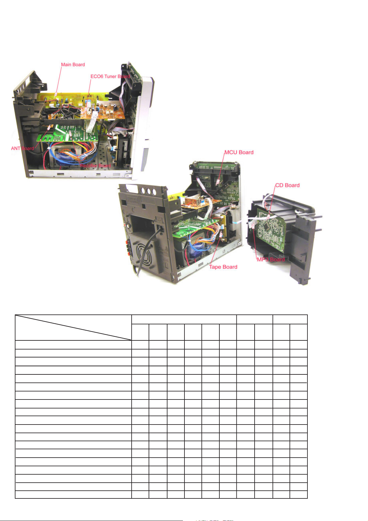
LOCATION OF PCBS
1-2
VERSION VARIATIONS:
Type /Versions: MCM510
Features &
Board in used:
Aux in / CDR in
Line Out
Video Out
Surround Out
Subwoofer Out
Power Booster Out
Digital Out
Digital in
Matrix Surround
RDS x x
News x x
Dolby Pro Logic (DPL)
Incredible Surround
Karaoke Features
Voltage Selector
ECO Power Standby (LCD Display Off) x x
ECO6 Tuner Board - Systems Non-Cenelec
ECO6 Tuner Board - Systems Cenelec
/22
x x
x x
xx
/25
/33
x
x
x
x
Page 3

SPECIFICATIONS
1-3
GENERAL:
Mains voltage :
230V ± 10% for /22/25
220V ± 10% for /33
Mains frequency : 50/60Hz
Clock accuracy : < 4 seconds per day
Dimension centre unit : 175(W) x 254(H) x 315(D) (mm)
Power consumption
Active : 15W
Standby : < 3W (DEMO mode off)
ECO Power Standby : < 1W for /22/25
TUNER:
FM
Tuning range : 87.5-108MHz
Grid : 50kHz
IF frequency : 10.7MHz ± 20kHz
Aerial input : 75 Ω coaxial
Sensitivity at 26dB S/N : < 22dBf
Selectivity at 300kHz bandwidth : > 33dB
Image rejection : > 20dB [> 25dB]
Distortion at RF=1mV, dev. 75kHz : < 3%
-3dB Limiting point : < 23.5dB
Crosstalk at RF=1mV, dev. 40kHz : > 26dB
MW
Tuning range : 531-1602kHz
Grid : 9kHz
IF frequency : 450kHz ± 1kHz
Aerial input : Frame aerial 18.1µH
Sensitivity at 26dB S/N : < 4.0mV/M
[> 3.25mV/M]
Selectivity at 300kHz bandwidth : > 20dB
IF rejection : > 24dB
Image rejection : > 20dB [> 28 dB]
Distortion at RF=50mV, M=80% : < 5%
AMPLIFIER:
Output power
L & R : 2 x 25W (4Ω, 1kHz, 10% THD)
Frequency response within -3dB : 60Hz-14kHz
Digital Sound Control (DSC) : Jazz / Rock / Pop / Classic
Dynamic Bass Boost (DBB) : ON / OFF
Input sensitivity
Aux in (at 1kHz) : 500mV at 600 Ω
Output sensitivity
Headphone output at 32 kΩ : 15mW ± 2dB (Max. vol.)
COMPACT DISC:
Frequency response within ± 3dB : 63Hz - 14kHz
Output level (in Vrms) : 500mV, Z
= 100Ω
out
Signal/Noise ratio (A-weighted) : > 65dBA
Distortion at 1kHz : < 0.02%
Channel unbalance at 1kHz : < ±2dB
Channel separation at 1kHz : > 30dB
Emphasis : 15/50 µS (switched
automatically by CD10)
THD Noise(1kHz) : < 1.0%
Outband Attenuation : > 35dB
MP3-CD Bit Rate : 8-320 kbps
WMA-CD Bit Rate
: 64-192 kbps
Sampling Rate : 8, 11.025, 12, 16, 22.05,
24, 32, 44.1, 48, 96 kHz
Format
: ISO9660, Joliet
CASSETTE RECORDER:
Number of track : 2 stereo
Tape speed : 4.76 cm/sec
±
2%
Wow and flutter : < 0.48% JIS
Fast-wind/Rewind time C60 : 130 sec
±
Bias system : 76kHz
10kHz
Rec/Pb frequency response within 8dB : 125Hz - 10kHz
Signal to Noise Ratio (Type I) : > 48dBA
LW
Tuning range : 153-279kHz /22
Grid : 3kHz
IF frequency : 450kHz ± 1kHz
Aerial input : Frame aerial
Sensitivity at 26dB S/N : [< 7.7mV/M]
Selectivity at 18kHz bandwidth : [> 24dB]
IF rejection : [> 24dB]
Image rejection : [> 20dB]
Distortion at RF=50mV, m=80% : [< 5%]
[....] Values indicated are for "ECO Cenelec Board" only.
Page 4
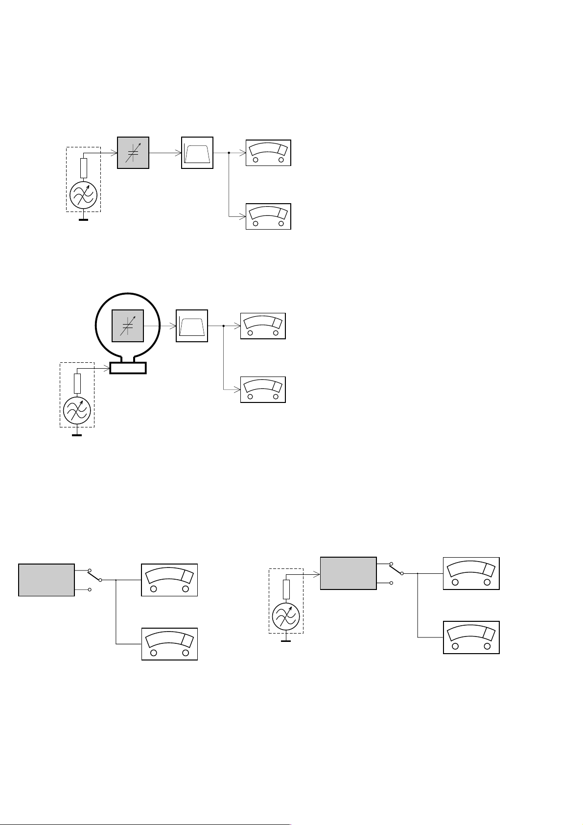
MEASUREMENT SETUP
Tuner FM
1-4
Bandpass
LF Voltmeter
e.g. PM2534
RF Generator
e.g. PM5326
DUT
250Hz-15kHz
e.g. 7122 707 48001
Ri=50Ω
S/N and distortion meter
e.g. Sound Technology ST1700B
Use a bandpass filter to eliminate hum (50Hz, 100Hz) and disturbance from the pilottone (19kHz, 38kHz).
Tuner AM (MW,LW)
RF Generator
e.g. PM5326
Ri=50Ω
DUT
Frame aerial
e.g. 7122 707 89001
Bandpass
250Hz-15kHz
e.g. 7122 707 48001
LF Voltmeter
e.g. PM2534
S/N and distortion meter
e.g. Sound Technology ST1700B
To avoid atmospheric interference all AM-measurements have to be carried out in a Faraday´s cage.
Use a bandpass filter (or at least a high pass filter with 250Hz) to eliminate hum (50Hz, 100Hz).
CD
Use Audio Signal Disc
(replaces test disc 3)
DUT
L
R
SBC429 4822 397 30184
S/N and distortion meter
e.g. Sound Technology ST1700B
LEVEL METER
e.g. Sennheiser UPM550
with FF-filter
Recorder
Use Universal Test Cassette CrO2 SBC419 4822 397 30069
or Universal Test Cassette Fe SBC420 4822 397 30071
LF Generator
e.g. PM5110
DUT
L
R
S/N and distortion meter
e.g. Sound Technology ST1700B
LEVEL METER
e.g. Sennheiser UPM550
with FF-filter
Page 5
SERVICE AIDS
1-5
Service Tools:
Universal Torx driver holder .................................. 4822 395 91019
Torx bit T10 150mm ............................................. 4822 395 50456
Torx driver set T6 - T20 ......................................... 4822 395 50145
Torx driver T10 extended ...................................... 4822 395 50423
Cassette:
SBC419 Test cassette CrO2 ................................. 4822 397 30069
SBC420 Test cassette Fe ..................................... 4822 397 30071
MTT150 Dolby level 200nWb/M ............................ 4822 397 30271
Compact Disc:
SBC426/426A Test disc 5 + 5A ............................ 4822 397 30096
SBC442 Audio Burn-in Test disc 1kHz ................. 4822 397 30155
SBC429 Audio Signals disc .................................. 4822 397 30184
Dolby Pro-logic Test Disc ...................................... 4822 395 10216
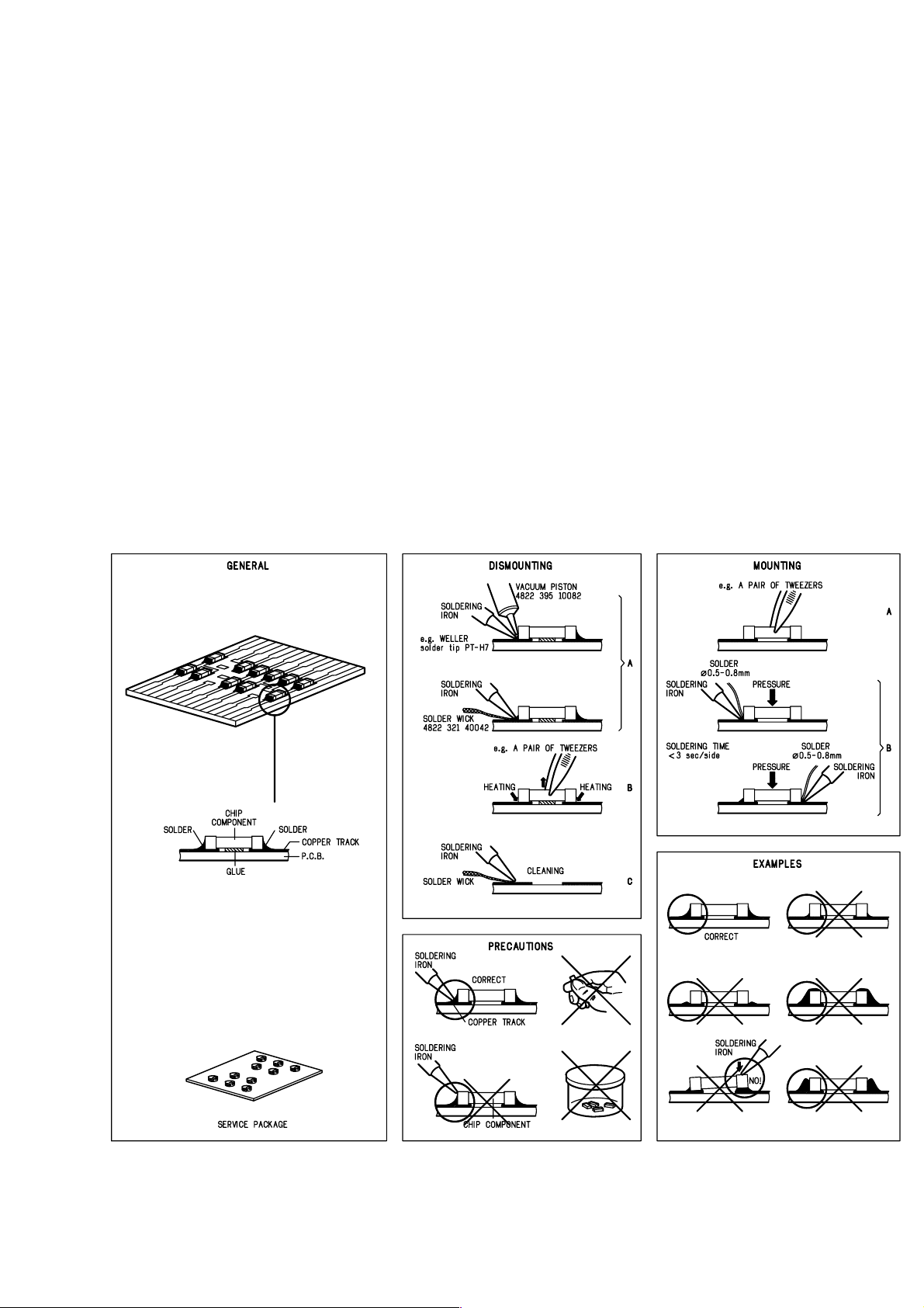
HANDLING CHIP COMPONENTS
ESD Equipment:
Anti-static table mat - large 1200x650x1.25mm ... 4822 466 10953
Anti-static table mat - small 600x650x1.25mm ..... 4822 466 10958
Anti-static wristband .............................................. 4822 395 10223
Connector box (1MΩ) ............................................ 4822 320 11307
Extension cable
(to connect wristband to conn. box) .................. 4822 320 11305
Connecting cable
(to connect table mat to conn. box) .................. 4822 320 11306
Earth cable (to connect product to mat or box) .... 4822 320 11308
Complete kit ESD3
(combining all above products) ......................... 4822 320 10671
Wristband tester .................................................... 4822 344 13999
Page 6

WARNING
GB
All ICs and many other semi-conductors are
susceptible to electrostatic discharges (ESD).
Careless handling during repair can reduce life
drastically.
When repairing, make sure that you are
connected with the same potential as the mass
of the set via a wrist wrap with resistance.
Keep components and tools also at this
potential.
F
ATTENTION
Tous les IC et beaucoup d’autres
semi-conducteurs sont sensibles aux
décharges statiques (ESD).
Leur longévité pourrait être considérablement
écourtée par le fait qu’aucune précaution n’est
prise à leur manipulation.
Lors de réparations, s’assurer de bien être relié
au même potentiel que la masse de l’appareil et
enfiler le bracelet serti d’une résistance de
sécurité.
Veiller à ce que les composants ainsi que les
outils que l’on utilise soient également à ce
potentiel.
1-6
ESD
D
WARNUNG
Alle ICs und viele andere Halbleiter sind
empfindlich gegenüber elektrostatischen
Entladungen (ESD).
Unsorgfältige Behandlung im Reparaturfall kan
die Lebensdauer drastisch reduzieren.
Veranlassen Sie, dass Sie im Reparaturfall über
ein Pulsarmband mit Widerstand verbunden
sind mit dem gleichen Potential wie die Masse
des Gerätes.
Bauteile und Hilfsmittel auch auf dieses gleiche
Potential halten.
WAARSCHUWING
NL
Alle IC’s en vele andere halfgeleiders zijn
gevoelig voor electrostatische ontladingen
(ESD).
Onzorgvuldig behandelen tijdens reparatie kan
de levensduur drastisch doen verminderen.
Zorg ervoor dat u tijdens reparatie via een
polsband met weerstand verbonden bent met
hetzelfde potentiaal als de massa van het
apparaat.
Houd componenten en hulpmiddelen ook op
ditzelfde potentiaal.
I
AVVERTIMENTO
Tutti IC e parecchi semi-conduttori sono
sensibili alle scariche statiche (ESD).
La loro longevità potrebbe essere fortemente
ridatta in caso di non osservazione della più
grande cauzione alla loro manipolazione.
Durante le riparazioni occorre quindi essere
collegato allo stesso potenziale che quello della
massa dell’apparecchio tramite un braccialetto
a resistenza.
Assicurarsi che i componenti e anche gli utensili
con quali si lavora siano anche a questo
potenziale.
GB
Safety regulations require that the set be restored to its original
condition and that parts which are identical with those specified,
be used.
NL
Veiligheidsbepalingen vereisen, dat het apparaat bij reparatie in
zijn oorspronkelijke toestand wordt teruggebracht en dat onderdelen,
identiek aan de gespecificeerde, worden toegepast.
F
Les normes de sécurité exigent que l’appareil soit remis à l’état
d’origine et que soient utiliséés les piéces de rechange identiques
à celles spécifiées.
D
Bei jeder Reparatur sind die geltenden Sicherheitsvorschriften zu
beachten. Der Original zustand des Geräts darf nicht verändert werden;
für Reparaturen sind Original-Ersatzteile zu verwenden.
“Pour votre sécurité, ces documents
doivent être utilisés par des spécialistes agréés, seuls habilités à réparer
votre appareil en panne”.
CLASS 1
LASER PRODUCT
GB
Invisible laser radiation when open.
Avoid direct exposure to beam.
Osynlig laserstrålning när apparaten är öppnad och spärren
är urkopplad. Betrakta ej strålen.
Warning !
S
Varning !
3122 110 03420
I
Le norme di sicurezza esigono che l’apparecchio venga rimesso
nelle condizioni originali e che siano utilizzati i pezzi di ricambio
identici a quelli specificati.
"After servicing and before returning set to customer perform a
leakage current measurement test from all exposed metal parts to
earth ground to assure no shock hazard exist. The leakage current
must not exceed 0.5mA."
Varoitus !
SF
Avatussa laitteessa ja suojalukituksen ohitettaessa olet alttiina
näkymättömälle laserisäteilylle. Älä katso säteeseen!
DK Advarse !
Usynlig laserstråling ved åbning når sikkerhedsafbrydere er
ude af funktion. Undgå udsaettelse for stråling.
Page 7
1-7
INFORMATION ABOUT LEAD-FREE SOLDERING
Philips CE is producing lead-free sets from 1.1.2005 onwards.
IDENTIFICATION:
Regardless of special logo (not always indicated) one must treat all sets from 1 Jan 2005 onwards, according next rules:
Example S/N:
• Use only lead-free solder alloy Philips SAC305 with order code 0622 149 00106. If lead-free solder-paste is required, please contact
the manufacturer of your solder-equipment. In general use of solder-paste within workshops should be avoided because paste is not
easy to store and to handle.
• Use only adequate solder tools applicable for lead-free solder alloy. The solder tool must be able
• Adjust your solder tool so that a temperature around
• Mix of lead-free solder alloy / parts with leaded solder alloy / parts is possible but PHILIPS recommends strongly to avoid mixed
• Use only original spare-parts listed in the Service-Manuals. Not listed standard-material (commodities) has to be purchased at
• Special information for BGA-ICs:
• For sets produced before 1.1.2005 (except products of 2004), containing leaded solder-alloy and components, all needed spare-parts
• On our website www.atyourservice.ce.Philips.com
o To reach at least a solder-temperature of 40
o To stabilize the adjusted temperature at the solder-tip
o To exchange solder-tips for different applications.
solder-joint should not exceed ~ 4 sec. Avoid temperatures above 400 otherwise wear-out of tips will rise drastically and flux-fluid
will be destroyed. To avoid wear-out of tips switch off un-used equipment, or reduce heat.
solder alloy types (leaded and lead-free).
If one cannot avoid or does not know whether product is lead-free, clean carefully the solder-joint from old solder alloy and re-solder
with new solder alloy (SAC305).
external companies.
- always use the 12nc-recognizable soldering temperature profile of the specific BGA (for de-soldering always use the lead-free
temperature profile, in case of doubt)
- lead free BGA-ICs will be delivered in so-called 'dry-packaging' (sealed pack including a silica gel pack) to protect the IC against
moisture. After opening, dependent of MSL-level seen on indicator-label in the bag, the BGA-IC possibly still has to be baked dry.
(MSL=Moisture Sensitivity Level). This will be communicated via AYS-website.
Do not re-use BGAs at all.
will be available till the end of the service-period. For repair of such sets nothing changes.
BGA-de-/soldering (+ baking instructions)
∗
Heating-profiles of BGAs and other ICs used in Philips-sets
∗
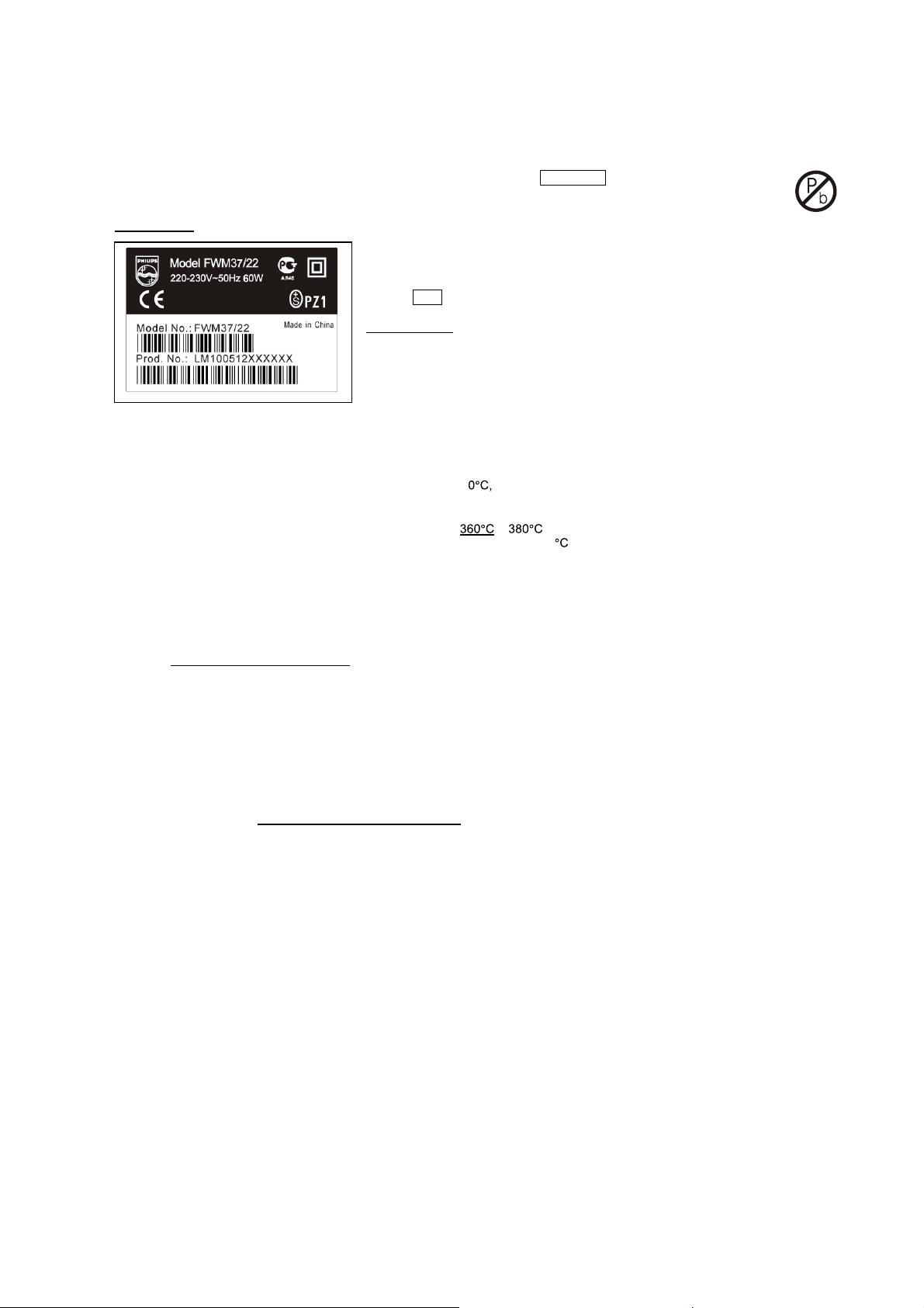
Bottom line of typeplate gives a 14-digit S/N. Digit 5&6 is the year, digit 7&8 is the week number,
so in this case 2005 wk12
So from 0501 onwards = from 1 Jan 2005 onwards
Important note
you avoid mixing solder-alloys (leaded/ lead-free). So best to always use SAC305 and the
higher temperatures belong to this.
Due to lead-free technology some rules have to be respected by the workshop during a repair:
: In fact also products of year 2004 must be treated in this way as long as
− is reached and stabilized at the solder joint. Heating-time of the
you find more information to:
For additional questions please contact your local repair-helpdesk.
You will find this and more technical information within the "magazine", chapter "workshop news".
SERVICE INSTRUCTION
Safety regulations require that after a repair, the set must be returned in its original condition. Pay in particular attention to
the following points:
· Route the wire trees correctly and fix them with the
mounted cable clamps.
· Check the insulation of the AC Power lead for external
damage.
· Check the strain relief of the AC Power cord for proper
function.
· Check the electrical DC resistance between the AC Power
Plug and the secondary side (only for sets which have a AC
Power isolated power supply):
1. Unplug the AC Power cord and connect a wire
between the two pins of the AC Power plug.
2. Set the AC Power switch to the "on" position (keep the
AC Power cord unplugged!).
3. Measure the resistance value between the pins of the
AC Power plug and the metal shielding of the tuner or
the aerial connection on the set. The reading should be
larger than 4.5 Mohm (For U.S. it should be between
4.2 Mohm and 12 Mohm).
4. Switch "off" the set, and remove the wire between the
two pins of the AC Power plug.
• Check the cabinet for defects, to avoid touching of any
inner parts by the customer.
Page 8
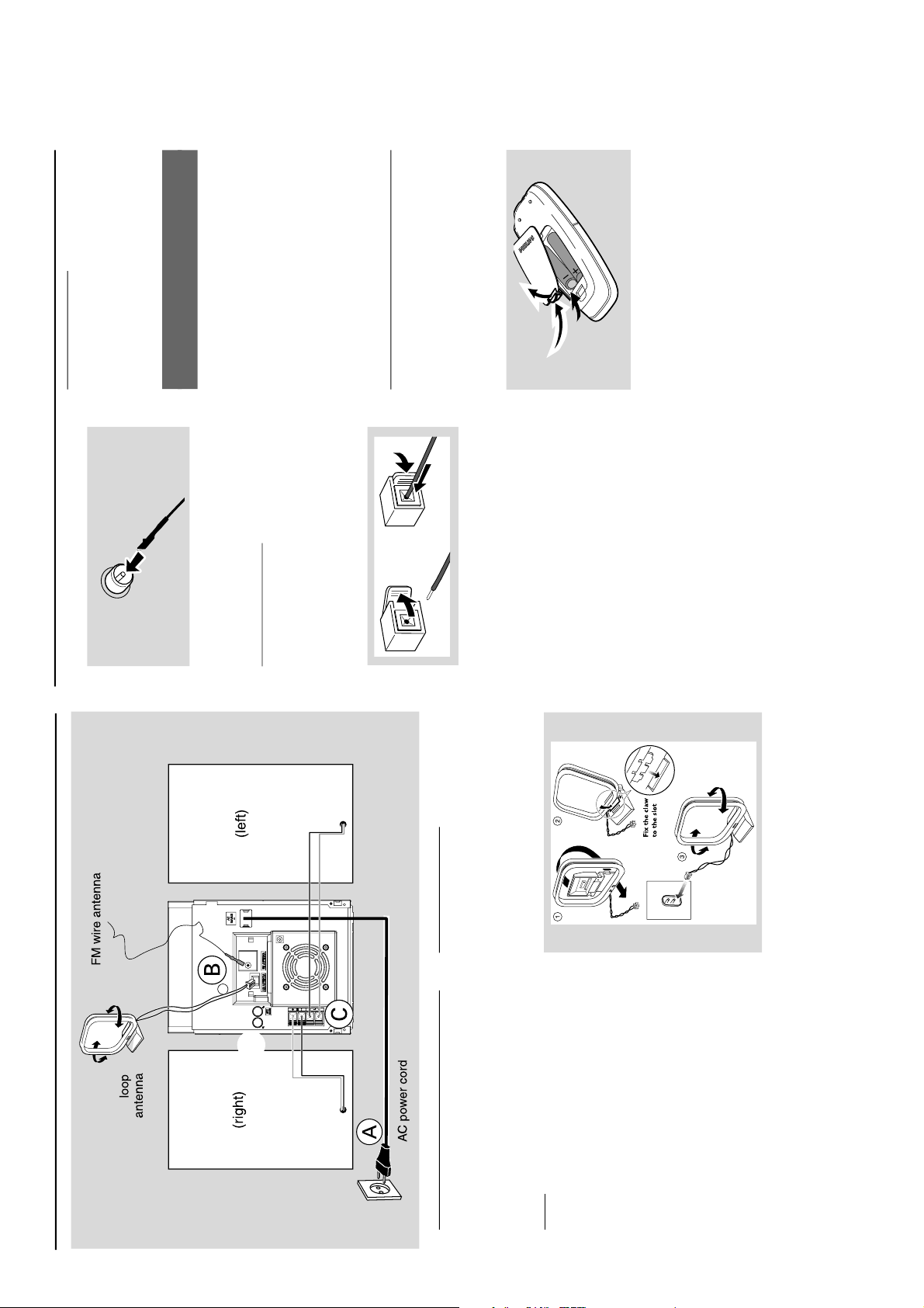
PREPARATIONS AND CONTROLS
Preparations
Rear connections
The type plate is located at the rear of the
system.
For users in the U.K.: please follow the
instructions on page 2.
A
Pow er
Before connecting the AC power cord to the
wall outlet, ensure that all other connections
have been made.
WARNING!
–For optimal performance, use only the
original power cable.
–Never make or change connections with
the power switched on.
To avoid overheating of the system, a safety
circuit has been built in. Therefore, your
system may switch to Standby mode
automatically under extreme conditions. If
this happens, let the system cool down
before reusing it (not available for all versions).
B
Antennas Connection
Connect the supplied MW loop antenna and FM
antenna to the respective terminals. Adjust the
position of the antenna for optimal reception.
MW Antenna
-
AM ANTENNA
Position the antenna as far as possible from a TV,
VCR or other radiation source.
MW
Speaker
Speaker
D
Preparations
FM Antenna
For better FM stereo reception, connect an
outdoor FM antenna to the FM AERIAL (FM
ANTENNA) terminal.
C
Speakers Connection
Front Speakers
Connect the speaker wires to the SPEAKERS
terminals, right speaker to "R" and left speaker to
"L", coloured (marked) wire to "+" and black
(unmarked) wire to "-".
1
2
Fully insert the stripped portion of the speaker
wire into the terminal as shown.
Notes:
–For optimal sound performance, use the
supplied speakers.
– Do not connect more than one speaker to any
one pair of
+
/
-
speaker terminals.
– Do not connect speakers with an impedance
lower than the speakers supplied. Please refer to
the SPECIFICATIONS section of this manual.
D
Optional connection
The optional equipment and connecting cords
are not supplied. Refer to the operating
instructions of the connected equipment for
details.
Connecting other equipment to your
system
Connect the audio left and right OUT terminals
of a TV, VCR, Laser Disc player, DVD player or
CD Recorder to the AUX IN terminals.
Note:
– If you are connecting equipment with a
monaural output (a single audio out terminal),
connect it to the AUX IN left terminal. Alternatively,
you can use a “single to double” cinch cable (the
output sound still remain monaural).
Inserting batteries into the
remote control
Insert two batteries (type R03 or AAA) into the
remote control with the correct polarity as
indicated by the "+" and "-" symbols inside
the battery compar tment.
CAUTION!
– Remove batteries if they are exhausted
or will not be used for a long time.
– Do not use old and new or different
types of batteries in combination.
– Batteries contain chemical substances, so
they should be disposed of properly.
1-8
Page 9

PREPARATIONS AND CONTROLS
VOLUME
MP3
-
CD/CD
-
R/CD
-
RW COMPATIBLE
INCREDIBLE
SURROUND
PROGRAM
TUNING
ALBUM
PRESET
SOURCE
TIMER SET
DBBDSC
OPEN/
CLOSE
RDS
CLOCK SETBAND
STANDBY
-
ON
ECO POWER
RECORD DISPLAY
MCM510 MICRO SYSTEM
iR
/
5
9
8
$
!
0
3
^
1
2
%
4
#
@
7
6
&
(
OPEN CLOSE
*
%
)
$
¡
8
6
#
@
7
™
9
£
24
25
Controls
Controls on the system and
remote control
1
Eco Power/STANDBY ON y
– to switch the system on or to Eco Power
standby/normal standby with clock display.
2
Display screen
– to view the current status of the system.
3
BAND/DISPLAY
for Tuner ............. to select waveband : FM, MW or
LW.
for CD/MP3-CD…to select disc information
display mode.
4
PROGRAM
for CD/MP3-CD…to programme disc tracks.
for Tuner ............. to programme preset radio
stations.
5
CLOCK SET/RDS
for Tuner ............. to activate RDS news.
for Clock ............ (on the system only) to set the
clock function.
6
TUNING S/T ( 5 /6)
for CD ................. to fast reverse/forward the disc.
for CD/MP3 CD…(on the system only) to select
a desired track.
for Tuner ............. to tune to a lower or higher
radio frequency.
for Tape ............... to rewind or fast forward.
7
ALBUM/PRESET/TIMER SET 4/3
for MP3-CD .....to select previous/next album.
for Tuner ............. to select a preset radio station.
for Timer Set (3) (on the system only) to set the
timer function.
8
STOP 9
for CD/MP3-CD…to stop playback or to clear a
programme.
for Tape ............... to stop playback or recording.
9
PLAY/PAUSE 2;
for CD/MP3 CD…to start or interr upt playback.
for Tape ............... to start playback.
0
Ta pe deck
!
OPEN/CLOSE 0
– to open tape compar tment.
@
DBB/INCREDIBLE SURROUND (IS)
– to create a super-enhanced stereo effect.
– to enhance the bass.
#
DSC (Digital Sound Control)
– to select the desired sound effect : OPTIMAL/
ROCK/POP/JAZZ.
$
VOLUME (VOL + / -)
– to increase or decrease the volume.
– (on the system only) to adjust the hours and
minutes for the clock/timer functions.
%
SOURCE
– to select the respective sound source : CD,
TUNER, TAPE or AUX.
^
RECORD
– to start recording.
&
iR sensor
– infrared sensor for remote control.
*
OPEN•CLOSE
– to open or close the disc tray.
(
n Headphone
– Plugs in the headphones jack. The speakers
output will be cancelled.
)
MODE
– to shuffle and repeat a track/disc.
¡
w /
– to select a desired track.
™
MUTE
– interrupts and resumes sound reproduction.
£
TIMER
– to activate/deactivate the timer function.
SLEEP
– to activate/deactivate or set the sleep timer.
∞
B
– to switch the system to standby mode.
Notes for remote control:
– First select the source you wish to control
by pressing one of the source select keys on
the remote control (for example CD,
TUNER).
– Then select the desired function (for
example 6 ,
w
,
).
24
w
0
w
1-9
Page 10

1-10
Cleaning the Cabinet
Use a soft cloth slightly moistened with a mild
detergent solution. Do not use a solution
containing alcohol, spirits, ammonia or abrasives.
Cleaning Discs
When a disc becomes dirty,
clean it with a cleaning cloth.
Wipe the disc from the centre
out.
Do not use solvents such as
benzene, thinner, commercially
available cleaners, or antistatic spray intended for
analogue records.
Cleaning the disc lens
After prolonged use, dirt or dust may
accumulate at the disc lens. To ensure good
playback quality, clean the disc lens with Philips
CD Lens Cleaner or any commercially available
cleaner. Follow the instructions supplied with
cleaner.
Cleaning the Heads and the Ta pe Paths
To ensure good recording and playback quality,
clean the heads
A
, the capstan(s)
B
, and
pressure roller(s)
C
after every 50 hours of
tape operation.
Caution: Do not rotate the heads during
cleaning.
Use a cotton swab slightly moistened with
cleaning fluid or alcohol.
You can also clean the heads by playing a
cleaning tape once.
A A
B
C
Demagnetizing the heads
Use a demagnetizing tape available at your
dealer.
Maintenance
“NO DISC” is displayed.
Radio reception is poor.
Insert a disc.
Check if the disc is inserted upside down.
Wait until the moisture condensation at the lens
has cleared.
Replace or clean the disc, see “Maintenance”.
Use a finalised CD-RW or CD-R.
If the signal is too weak, adjust the antenna or
connect an external antenna for better
reception.
Increase the distance between the Micro HiFi
System and your TV or VCR.
WARNING
Under no circumstances should you try to repair the system yourself, as this will
invalidate the warranty. Do not open the system as there is a risk of electric shock.
If a fault occurs, first check the points listed below before taking the system for repair. If
you are unable to remedy a problem by following these hints, consult your dealer or
Philips for help.
Problem
Solution
Troubleshooting
Recording or playback cannot be made.
“CHK TAPE” is displayed.
The tape deck door cannot open.
The system does not react when buttons
are pressed.
Sound cannot be heard or is of poor
quality.
The left and right sound outputs are
reversed.
The remote control does not function
properly.
The timer is not working.
The Clock/Timer setting is erased.
Clean deck parts, see “Maintenance”.
Use only normal (IEC I) tape for recording.
Apply a piece of adhesive tape over the missing
tab space.
Remove and reconnect the AC power plug and
switch on the system again.
Remove and reconnect the AC power plug and
switch on the system again.
Adjust the volume.
Disconnect the headphones.
Check that the speakers are connected correctly.
Check if the stripped speaker wire is clamped.
Make sure the MP3-CD was recorded within
32-256 kbps bit rate with sampling frequencies
at 48 kHz, 44.1 kHz or 32 kHz.
Check the speaker connections and location.
Select the source (CD or TUNER, for example)
before pressing the function button
().
Reduce the distance between the remote
control and the system.
Insert the batteries with their polarities
(+/– signs) aligned as indicated.
Replace the batteries.
Point the remote control directly toward
IR sensor on the front of the system.
Set the clock correctly.
Press TIMER SET 3 (TIMER on the remote
control) to switch on the timer.
If a recording is in progress, stop the recording.
Power has been interrupted or the power cord
has been disconnected. Reset the clock/timer.
Problem
Solution
Tr oubleshooting
6 ,
w
,
w
Page 11

DISMANTLING INSTRUCTIONS
2-1
2-1
Dismantling of the Cover Cassette and Universal Loader
1) Push 1 catch each on the left & right side then remove
the Cover Cassette in the direction as shown in Figure 1
and Figure 1A.
2) Loosen 4 screws to remove the Cover Top by sliding
it out towards the rear before lifting up.
-2 screws on the rear
-1 screw each on the left & right side
3) Loosen 2 screws each to remove the Panel Left and
Panel Right. The Panels are removed by sliding it
towards the rear and outwards.
-1 screw on the rear
-1 screw on the side
- see Service position A
6) Loosen 2 screws A (see Figure 2) to remove the Bracket
Module Mounting and CD Module.
-1 screw each on the left & right side
Detaching the Front Panel assembly from the Bottom/Rear assembly
Lift up and out
Figure 1
Push catches on two sides
Figure 1A
Detaching the Front Panel assembly from the Bottom/Rear assembly
1) Remove 2 screws B (see Figure 3) from the bottom of the
Cabinet Front.
2) Release the fixation of the Combi Board (pos1102-1003)
to Bracket Combi (pos 155) by releasing the 2 catches C1
(see Figure 7) and pulling the Combi Board outwards as
shown in Figure 7A.
3) Uncatch 2 catches C2 (see Figure 7) on the left & right
sides of the Cabinet Front (pos 101) and slides the Front
Panel assembly out towards the front.
- see Service position C
A
Figure 2
Figure 4A
Dismantling of the Front Panel assembly
1) The Knob Volume can be remove by pulling it out
in the direction as shown in Figure 5.
2)
Loosen 3 screws C (see Figure 6) to remove the Bracket
Front Cabinet Display.
3)
Loosen 3 screws D (see Figure 6) to remove Front
Display Board.
4)
Loosen 2 screws E (see Figure 6) to remove the
Headphone Board.
5)
Loosen 4 screws F (see Figure 7) to remove the Module
Tape Deck.
Figure 4
Figure 5
B
Figure 3
Page 12
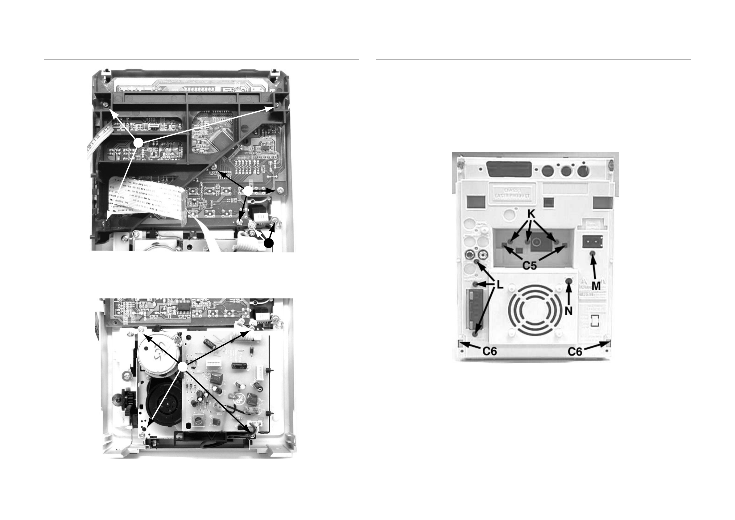
DISMANTLING INSTRUCTIONS
2-2
2-2
Dismantling of the Front Panel assembly
C
D
Dismantling of the Rear Panel assembly
1) Loosen 3 screws K and 2 catches C5 (see Figure 8) to
remove the Tuner Board assembly.
2) Loosen 3 screws L (see Figure 8) to free the Main
Board.
3) Loosen 1 screw M (see Figure 8) to free the Mains
Socket Bracket.
4) Loosen 1 scew N and 2 catches C6 (see Figure 8) to
free the Panel Rear by sliding it out towards the rear.
Note : Tuner Board assembly and Mains Socket Bracket
can also be removed together with the Panel Rear..
Figure 6
F
E
Figure 8
Figure 7
Page 13
DISMANTLING INSTRUCTIONS
2-3 2-3
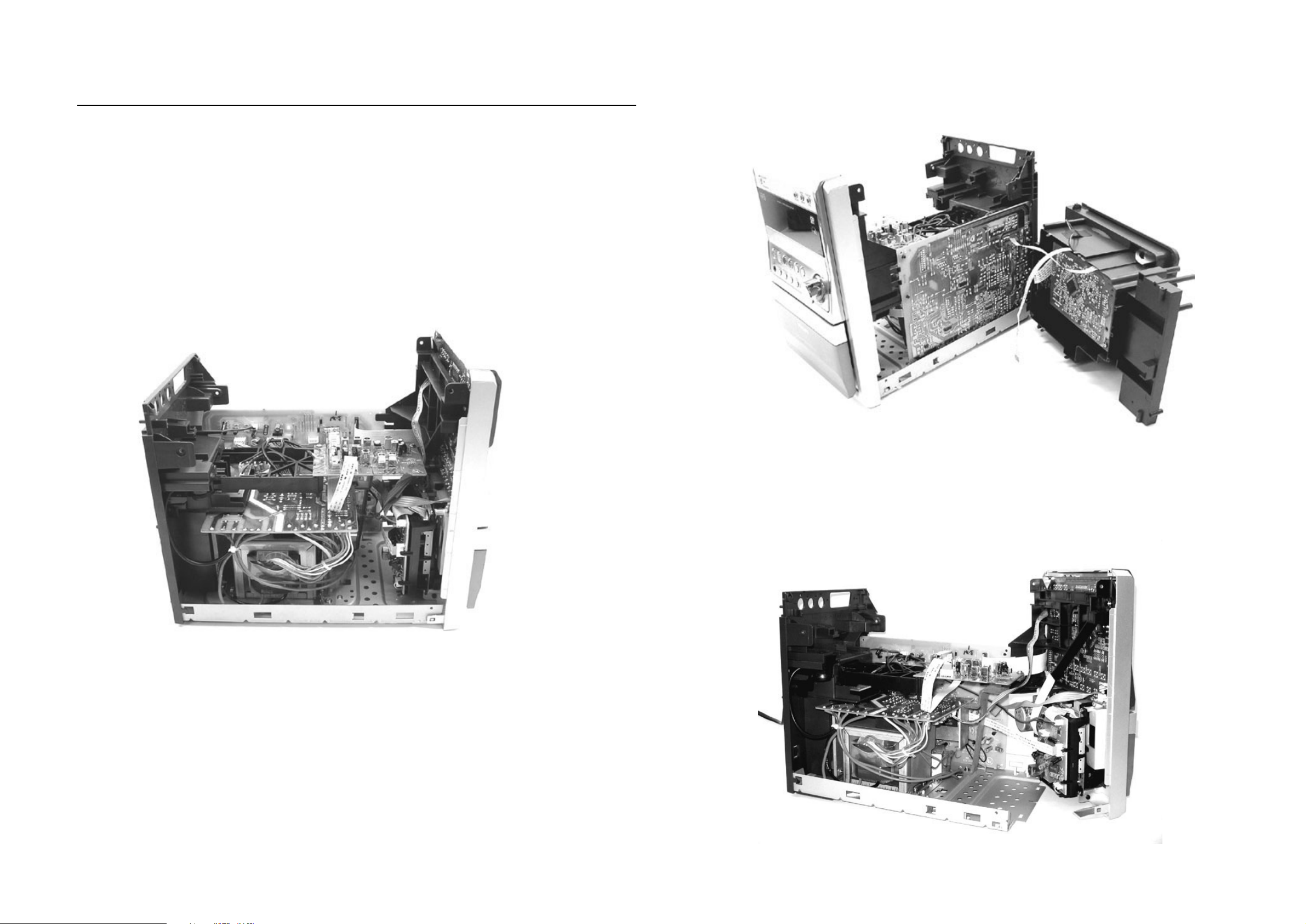
Repair Hints & Service Positions
1) During repair it is possible to disconnect the Tuner Board
and/or CD Module completely unless the fault is sus-
pected to be in that area. This will not affect the
performance of the rest of the set.
Service position A
Service position B
Note: The flex cables are very fragile, care should be taken
not to damage them during repair. After repair, be
very sure that the flex cables are inserted properly
into the flex sockets before encasing, otherwise faults
may occurs.
Service position C
Page 14
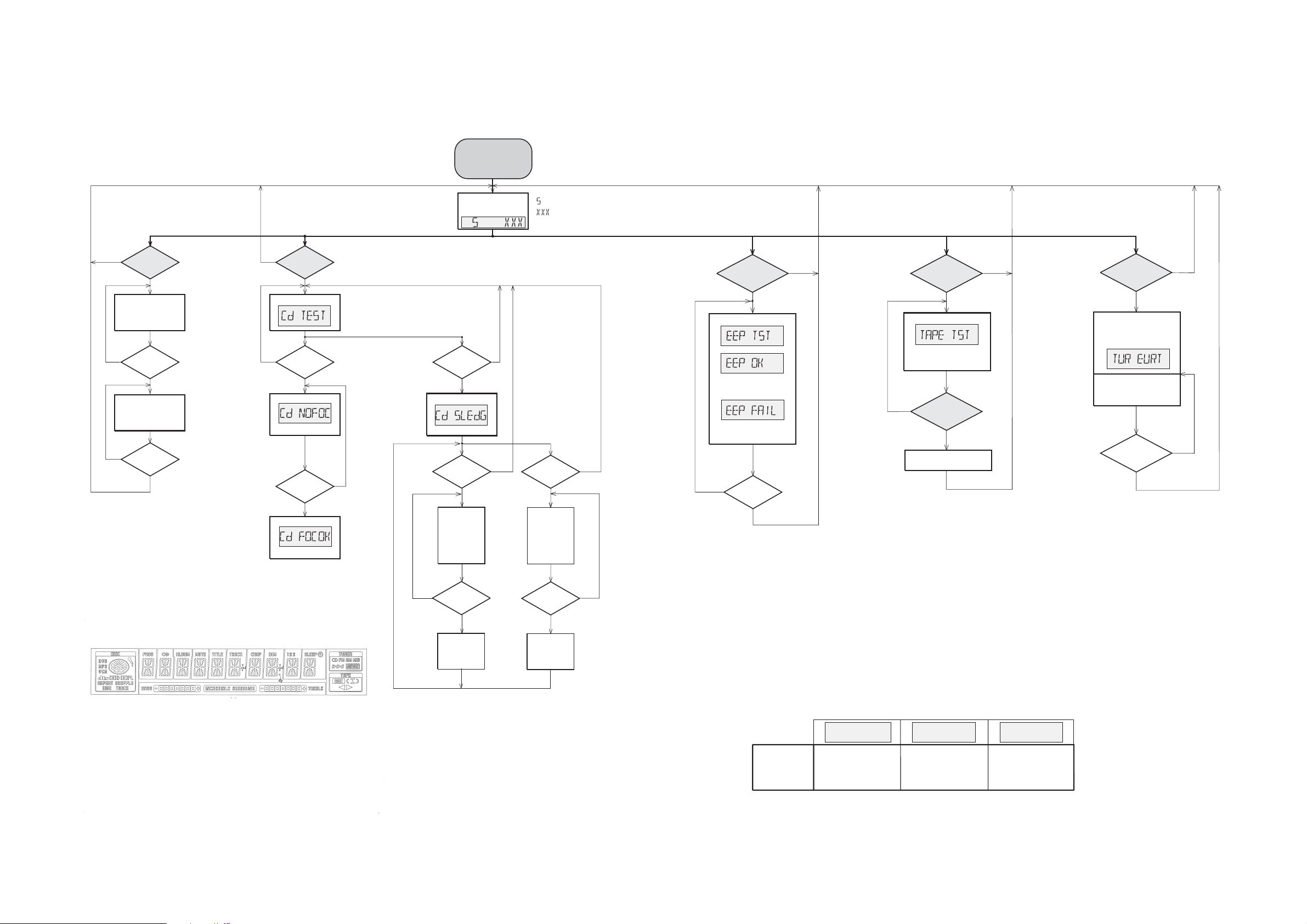
SERVICE TEST PROGRAM
3-1
3-1
DISPLAY TEST
PLAY button
N
pressed?
Y
Display shows all
segments and flags
for checking open circuits.
see figure 1
N
PLAY button
pressed?
Y
BLANK
STOP button
N
pressed?
Y
CD SERVO TEST
NEXT button
N
pressed?
Display shows
N N
ALBUM UP
pressed?
FOCUS search
Display shows
Enter focus test
FOCUS found?
Display shows
disc motor turns
STOP button pressed in any step returns
to begin of Service Testprogram.
Y
SLIDE MOTOR test
Y
N
Y
To enter Service
Testprogram hold
PLAY & DISPLAY buttons
depressed while
plugging mainscord in.
Display shows
version number
of the µP - software.
ALBUM DN
pressed?
Y
Display shows
Enter sledge test
NEXT button
pressed?
Y
Slide moves
outwards as
button
long as
is held
depressed.
Door switch is ignored → CD door can be opened.
*
Tuner test the sound settings Volume up/down,
*
DSC, IS and DBB function as in normal mode,
but flags will not be indicated on the display in all steps.
stands for Service mode,
is software version, eg. S 1262
FORMAT EEPROM
DISPLAY
button
pressed?
Y
Display shows
skip to
if it is fail,
skip to
EEPROM is cleared and
default values are stored.
N
PREV button
pressed?
Y
Slide moves
inwards as
button
long as
is held
depressed.
N
STOP button
N
pressed?
Y
This test should be done at the
end of the production process
N
TAPE TEST
REC button
Display shows
Solenoids of the deck
are activated for 2s and
deactivated for 3s.
N
PLAY/DISPLAY button
Switch all actions off
pressed?
Y
pressed?
Y
N
SOURCE TEST
PRESET UP
Display shows version
of tuner board as long as
PROGRAM
e.g.
Tuner is normal working
except for the PROGRAM
button.
STOP button
pressed?
N
key will be
pressed.
pressed?
Y
N
N
so that every set is customised
before leaving factory.
Figure 1
N
PLAY button
pressed?
Y
Slide stops
moving
PLAY button
pressed?
Y
Slide stops
moving
N
TUNER VERSIONS
REGION
&
SET VERSIONS
TUN EURT
EUROPE
FM/MW
/22/25
TUN USA
USA
FM/MW
/37 / 21/21M/30
table 2
TUN OSE
OVERSEAS
FM/MW
1)
Grid switchable
100/10kHz - 50/9kHz
Page 15
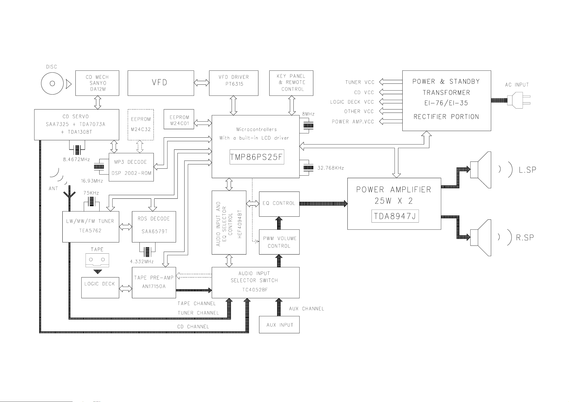
SET BLOCK DIAGRAM
4-1
4-1
Page 16

SET WIRING DIAGRAM
(
)
Front PCB
5-1
5-1
Page 17

6-1
FRONT BOARD
6-1
LAYOUT DIAGRAM - HEADPHONE BOARD
TABLE OF CONTENTS
Headphone Board Layout ............................................... 6-1
Front Board Layout Top View .......................................... 6-2
Front Board Layout Bottom View .................................... 6-3
Circuit Diagram ................................................................ 6-4
Electrical Parts List .......................................................... 6-5
Page 18

LAYOUT DIAGRAM - FRONT BOARD
TOP SIDE
6-2
6-2
Page 19

LAYOUT DIAGRAM - FRONT BOARD
BOTTOM SIDE
6-3
6-3
Page 20

CIRCUIT DIAGRAM - FRONT BOARD
6-4
6-4
/22/25
Page 21

ELECTRICAL PARTS - FRONT BOARD
EN701 9940 000 03211 ENCODER
IC701 9940 000 03213 IC OTP TMP86PS25F
IC702 9940 000 03272 IC M24C01-RDW6T
IC703 9940 000 03215 RDS IC SAA6581T
IC704 9940 000 03214 VFD DRIVER IC PT6315
L703 9940 000 03216 CHOKE COIL 100µH
L705 9965 000 17286 FIXED INDUCTOR 0.47µH-K
LED701 9940 000 01442 LED 5.25X2.9 RED 3R4SDC-8
RS701 9940 000 03271 IR RECEIVER
SW701 9965 000 13779 TACT SWITCH
SW702 9965 000 13779 TACT SWITCH
SW703 9965 000 13779 TACT SWITCH
SW704 9965 000 13779 TACT SWITCH
SW705 9965 000 13779 TACT SWITCH
SW706 9965 000 13779 TACT SWITCH
6-5
6-5
SW707 9965 000 13779 TACT SWITCH
SW708 9965 000 13779 TACT SWITCH
SW709 9965 000 13779 TACT SWITCH
SW710 9965 000 13779 TACT SWITCH
SW711 9965 000 13779 TACT SWITCH
SW712 9965 000 13779 TACT SWITCH
SW713 9965 000 13779 TACT SWITCH
SW714 9965 000 13779 TACT SWITCH
VFD701 9940 000 03212 VFD HNA-13SM42T
X701 9940 000 03209 CRYSTAL 4.332MHZ
X702 9940 000 03207 CERAMIC FILTER 8.0MHZ +-5%
X703 9940 000 03208 CRYSTAL 32.768KHZ 12.5PF
Note: Only these parts mentioned in the list are normal
normal service parts.
Page 22

7A-17A-1
1
FM
Osc.
FM
Mixer
AM
Mixer
AM
Osc.
AM IF
IF1
IF2
FM
Det.
AM
Det.
3393733
RADIO IC
TEA 5757H
TUNER BOARD
ECO 6
Systems
1018 11
14
15
24
right
right
left
left
stereo
VCO
4140 36 193244 25
Stereo
Decoder
AFC
AFC +
AFC -
4
4
AGC
Pre-
scaler
Multi-
plexer
Charge
pump
Stabilizer
CONTROL
Reference
Oscillator
29
28
27
clock
data
enable
P1
P0
31
30
programmable
output ports
V
Loop
V
Loop
V
Loop
V
Loop
V
Loop
2
6
5
43
C
D
450kHz450kHz450kHz
20
75kHz
V
Stab
AV
Stab
BV
Stab
B
V
Stab
A V
Stab
B
10,7 MHz 10,7 MHz
35 9
Vdd Vcc1
723
V
Stab
A
V
Stab
B
38
34
22
Vcc2
8
ECO6 Systems, 140499
LF filter
RDS
(MPX)
RDS
(MPX)
stereo
clock
data
enable
Version
1120
1
8
FM
Frontend
AM
Frontend
AM-FRAME AERIAL
B
1103
1101
(1102)
A
FM
MPX
buffer ampl.
5
Discriminator
10,7 MHz
Vdd
Vcc1
Vcc
Vcc2
AM-RF
AM-Osc.
FM-Osc.
FM-RF FM-IF 1 FM-IF 2
AM-IF 1 AM-IF 2
AM-AFC
3
2
BLOCK DIAGRAM
ECO6 Tuner Board
version:
SYSTEMS non-CENELEC
TABLE OF CONTENTS
Blockdiagram ..................................................................7A-1
Schematic Diagram.........................................................7A-2
Component Layout..........................................................7A-3
Adjustment table .............................................................7A-3
Electrical Partslist............................................................7A-4
Page 23

7A-2 7A-2
ECO6 Sys-non Cenelec, 000911
1101 A1
1102 B1
1103 F2
1120 E14
1130 A2
1131 B2
1132 G13
2101 B3
2102 B1
2103 C7
2104 B3
2105 A2
2106 F3
2107 F4
2119 H6
2120 G6
2124 H6
2125 H6
2126 F7
2127 E7
2128 C8
2129 C7
2130 F11
2131 G8
2132 G8
2133 G8
2134 H8
2135 H9
2136 G14
2137 G13
2138 F9
2139 G9
2140 G9
2141 F10
2143 G12
2144 G11
2145 F12
2146 E12
2147 E12
2148 E12
2149 H7
2150 A10
2152 E4
2153 E5
2154 D5
2155 D5
2159 F6
2161 C11
2163 D11
2164 F10
2165 C7
2166 E11
2167 E11
2169 H8
3101 E4
3102 D4
3103 C6
3104 A7
3105 B6
3132 G5
3134 H6
3141 E7
3142 E7
3143 G7
3144 H7
3145 F8
3146 G13
3152 G14
3153 G13
3154 G13
3155 G11
3156 C12
3157 C12
3158 E13
3159 D13
3160 D12
3161 D13
3167 F12
3168 F11
3169 E11
3170 C12
3172 G12
3176 G7
3181 E6
5102 F2
5109 B9
5110 B10
5111 A8
5112 A11
5114 B11
5119 G9
5121 E11
5123 G5
5130 E5
5131 C6
6103 B2
6105-1 F3
6105-2 G5
6106 C3
6107 G13
6120 C13
6130 E5
6131 D5
7101 C8
7102 C6
7103 H7
7111 C13
7112 G12
T102 B2
T103 B2
T105 F2
T106 F2
T109 B6
T110 F5
T111 F4
T112 F7
T113 A8
T114 B10
T115 A8
T116 F10
T117 G13
T118 G11
T120 F13
T121 F13
T122 F13
T123 E13
T124 G14
T125 F14
T126 F13
T127 F13
T128 D7
T140 F11
T141 F10
T142 F10
1
34
6
87
2
1
34
6
87
2
LEGEND
p ...for provision only
USA ... for USA version only
E-EU ... for East European version only
22n
USA
22n
USA
p
p
p
7
1
2
3
8
6105
6
HN1V02H
54
3
6
1
2
7
29
25
13
30
31
16
4
42
15
1
7
22
9
23
38 34
2118
37 35
33
43 39
5
3
8
171412
24
11
10
2019
44
32
41 3640
6
2
27
28
26
1
3
4
5
6
87
2
1
34
6
87
2
1
34
6
87
2
p
SCALER
MULTI-
PLEXER
CONTROL
FILTER
AM
IF
AM
DET
FM
DET
VSTABB
DECODER
CHARGE
PUMP
AGC
OSC
AM DET
FM
IF2
RIPPLE
AGC
STABILIZER
AFC
VDD
VSTABA
AM-IF
MONO/
FM
FRONTEND
CONTROL
XTAL
AGC
PRE-
CTRL
AGC
AM
OSC
AGC
VCC2
FM
OSC
AM
MIXER
MIXER
FM
FM
IF1
FRONTEND
AM
STEREO
STEREO
RDS only
DISCRIMINATOR
to/from
FM-OSCILLATOR
PROGR.
MPX
Q-multiplier
MW
OUTPUT PORTS
to 1120
pin 5
ENABLE/MPX
BUFFER
kHz
VERSION DETECTION
VCO
RIGHT
14
12 3
AM FRAME AERIAL
DATA
C
D
E
F
AM-OSCILLATOR
FM 75 OHM
FM-IF2
MW
2345
AM-RF
450kHz
450kHz
AM-IF2
from 2169
78
AM-AFC
LEFT
6 7 8 9 10 11 12 13
456
FM-RF
TUNER BOARD ECO6
/ SYSTEMS NON CENELEC
9 1011121314
A
B
G
H
A
B
1
VCC
STEREO
CLOCK
AMPLIFIER
GND
H
C
D
E
F
G
470n
2132
BAS216
6120
2103
1u
2107
1n
3134
22K
6105-2
HN1V02H
100n
2163
T141
7KL
1K
3144
5102
3157
100K
T109
470R
3153
2130
22n
220R
3105
3142
100K
3167
120R
33p
2149
2K2
3145
1132
C-PAD
T103
T111
2164
470n
T102
2140 15p
2139
2138
2u2
82p
2133
1u
3103
8K2
T120
4p7
2154
3156
1101
USA
YKD21
100K
2161
100n
5119
2119
10p
T142
5123
11p
2106
3172
6106
BAS216
100n
2165
5K6
3154
3155
220R
330R
2124
33K
3176
22n
WRITE-EN
5114
7P
MUTE
P0
P1
PILOT
RF-GND1
RF-GND2
RIGHT
RIPPLE
VCC1
VCC2
VCO
VDD
VSTABA
VSTABB
FM-DEMOD
FM-IF1-IN
FM-IF2
FM-IF2-IN
FM-IN
FM-MIXOUT
FM-OSC
FM-RF
I-TUNE
IF-GND
LEFT
LPF
MPX-IN
AF-OUT
AFC+
AFC-
AGC
AM-AFC
AM-IF1-IN
AM-IF2
AM-MIXOUT
AM-OSC
AM-RF
CLOCK
DATA
DIG-GND
FIELDSTR-IND
5130
T127
T126
220n
2127
5121
DT-381
150K
3169
75K
3102
100K
56K
3141
1131
C-PAD
3132
5112
7P
6107
47R
6131
1SV228
BZX284-C11
1120
FE-BT-VK-N
T118
T140
T117
T112
2131
470n
33K
3101
1SV228
6130
3168
120R
2125
560p
T116
2n2
2148
100n
2141
470R
18p
2120
470R
3158
3152
3159
XH-S
1103
3160
470R
470R
220n
2143
2150
T125
1
2
3
4
5
6
7
8
22R
3146
BF550
7102
5131
11p
2155
O
100K
5110
G
I
1102
not USA
3170
T122
2135
15n
2167
2145
220p
T110
12p
HN1V02H
1n
2166
T105
6105-1
T106
T121
T123
BC547C
7112
3143
2129
100u
C-PAD
1130
22K
220n
2137
T128
3181
1K
330p
2126
2101
47p
BAV99
6103
2104
100p
2153
15p
T124
2152
33n
560p
E-EU
12p
E-EU
2p2
J
33p
2159
220p
2146
2169
2n2
1u
15n
2134
2144
220n
2136
22K
3161
BC857C
BC847C
7111
7103
2147
220p
VCC2
VCC2
VDD
T114
MPX
P1
P0
P1
VDD
MPX
VCC1
VCC1
VCC1
printed
printed
printed
1
2
13
2
1
2
3
1
2
TEA5757H
TEA5759H
J
7101
2128
10u
7111
component mounted
/14 FM-OIRT/MW
/00 /02 FM/MW/LW
6120 3170
/01 FM/MW
VERSION
/00 /02 FM/MW
3156
/17 FM/AM
/06 FM-Japan/AM
3157
VERSION PROGRAMMING COMPONENTS
J ... for Japanese version only
AM-IF1
450kHz
8
5111
1
2
3
4
6
7
T113
T115
FM-IF1
2
G
1I3
O
5109
3104
330R
100n
0R
4103
...V MW mode
...V LW mode
voltages measured while
set is tuned to a strong transmitter
...V FM mode stereo
EVM
V
5V
0V
152kHz, 50mV
pp
stereo stereomono
9.6V
9.5V
9.5V
10.4V
12V
1V
1.3V
1.4V
stereo 0.2V
mono 4.8V
9.6V
12Vtyp
stereo 0.4V
0.15V
11.1V
7.8V
2V
0.7V
0V
1.2V
7.6V
(10-14V)
0.2V
0V
1.2V
0.1V
D
1.4V
0.7V
4
0V
0V
mono 4.8V
1.4V
9.6V
1.4V
0.2V
0.7V
1.4V
7.9V
7.7V
0V
0V
0V
0V
0.6V
0.8V
0.1V
1.6-8V
1-8V
11.1V
0V
1V
1.4V
1.4V
B
7.6V
5
3
2
A
1.3V
0.7V
7.8V
11.1V
0.8V
0.6V
0.6V
1V
0.7V
1V
1.1V
1.1V
0V
0V
2V
C
1
0.8V
1.2V
1.1V
IF-AMP.
BFS20
7119
J
1K
3113
J
2112
J
100p
330R
3119
J
Signal path
FM
AF - left/right
AM
MPX (Audio Frequency)
2102
100n
2105
USA
100n
Page 24

7A-37A-3
VARICAP ALIGNMENT
FM RF
FM IF
VCO
AM IF
AM RF
3)
108MHz
87.5MHz
(65.81MHz)
87.5MHz
(65.81MHz)
87.5MHz
(65.81MHz)
279kHz
153kHz
1602kHz
531kHz
5130
check
5122
check
5123
check
8V ±0.2V
4.3V ±0.5V
(1.2V ±0.5V)
8V ±0.2V
1.1V ±0.4V
8V ±0.2V
1.1V ±0.4V
1494kHz
558kHz
560kHz 5102
1500kHz
5103198kHz
1494kHz
558kHz
560kHz
1500kHz
198kHz
2106
5102
2106
3142 152kHz ±1kHz
1)
98MHz
5112
MAX
FM
87.5 - 108MHz
(65.81 - 74, 87.5 - 108MHz)
LW
153 - 279kHz
MW
FM/MW/LW- version, 9kHz grid
531 - 1602kHz
1700kHz
530kHz
5123
check
8V ±0.2V
1.1V ±0.4V
1602kHz
531kHz
5123
check
6.9V ±0.2V
1.1V ±0.4V
108MHz
108MHz 2155
5131
MW
FM/AM-version, 10kHz grid
530 - 1700kHz
FM
MW
LW
98MHz, 1mV
continuous wave
450kHz
connect pin 6 of
IC 7101 (AM Osc.)
with 3.3kΩ to Vcc
Use Service Testprogram. By selecting the TUNER TEST test frequencies will be stored as preset frequencies automatically.
4
1
3
5
5
A
A
5119FM
10.7MHz, 45mV
continuous wave
2D
mod=1kHz
∆f=±22.5kHz
1)
If sensitivity of frequency counter is too low adjust to max. channel separation
(input signal: stereo left 90% + 9%, adjust output on right channel to minimum)
Repeat
ECO6, Sys + PA with frame aerial, 070799
TUNER ADJUSTMENT TABLE ( ECO6 FM/MW- and FM/MW/LW - versions with AM-frame aerial )
∆f=±10kHz
VRF = 0.5mV
C
see
remark
2)
220R
100nF
36
IC 7101
220R
100nF
40
IC 7101
2141
shortcircuit
to block AFC
21
IC 7101
max.
symmetric
f
o
AM AFC
MW
C
continuous wave
VRF = 2mV
5111
5114
2
0 ± 2 mV DC
0 ± 3 mV DC
MW
4)
FM/MW/LW- and FM/MW-version
( 9kHz grid)
531 - 1602kHz
B
∆f = ±30kHz
V
RF
as low as
possible
max.
symmetric
f
o
MW
FM/AM-version, 10kHz grid
530 - 1700kHz
3)
For AM RF adjustments the original frame antenna has to be used !
2)
RC network serves for damping the IF-filter while adjusting the other one.
4)
MW has to be aligned before LW.
Waverange Input frequency Input Tuned to Adjust Output Scope/Voltmeter
FM
87.5 - 108MHz
(65.81 - 74, 87.5 - 108MHz)
FM/MW-version, 9kHz grid
531 - 1602kHz
(as low as
possible)
ECO6 System non Cenelec stage .3, 120900
TUNER BOARD ECO6
Systems non Cenelec
/ componentside view
1101 A6
1102 B6
1103 D6
1120 A4
1130 B5
1131 D5
1132 A5
2106 C5
2107 B5
2128 C4
2129 B4
2133 D2
2138 C2
2144 B2
2155 C4
3142 D2
5102 D6
5109 A3
5110 B3
5111 B4
5112 A3
5114 A2
5119 C2
5121 B2
5123 D5
5130 D3
5131 D4
7112 C1
9101 A2
9103 B2
9104 B5
9105 B1
9106 B3
9107 D4
9108 C4
9109 D2
AM FRAME AERIAL
FM 75Ω
B
A
TUNER BOARD ECO6
Systems - non Cenelec
/
copperside view
2101 B4
2102 B1
2103 D4
2104 B4
2105 C1
2112 B5
2119 D3
2120 D3
2124 D3
2125 D3
2126 D6
2127 C5
2130 D5
2131 C5
2132 D6
2134 D7
2135 D7
2136 A4
2137 A4
2139 C6
2140 C6
2141 C6
2143 C7
2145 A5
2146 B7
2147 A5
2148 B6
2149 D6
2150 B5
2152 C5
2153 C5
2154 C4
2159 C5
2161 A6
2163 B6
2164 C6
2165 C4
2166 B6
2167 B6
2169 A4
3101 D5
3102 C3
3103 C4
3104 B4
3105 C4
3113 B5
3119 B5
3132 D5
3134 D3
3141 C5
3143 D6
3144 B7
3145 C5
3146 C7
3152 A4
3153 A4
3154 C7
3155 C7
3156 A6
3157 A6
3158 A4
3159 A5
3160 A5
3161 A5
3167 B7
3168 C7
3169 B6
3170 A6
3172 C7
3176 D6
3181 D4
4103 B5
4106 C4
4107 C5
4108 C5
6103 B3
6105 C3
6106 C3
6107 C7
6120 A6
6130 D4
6131 C4
7101 C5
7102 D4
7103 D7
7111 A5
7119 B5
These assembly drawings show a summary of all possible versions.
For components used in a specific version see schematic diagram respectively partslist.
ECO6 Systems non CENELEC stage .3, 120900
41..
in schematic diagram)
(not all items shown
SMD jumper
EB
C
A
K
1
2
7
8
4
D
A
C
1
2
5
3
V
dd
Vcc2
Vcc1
Page 25

MISCELLANEOUS
–––––––––––––––––––––––––––––––––––––––––––––––––––––
1101 2422 015 19376 SOCKET 2P CLICKFIT USA only
1102 4822 267 10283 SOCKET COAX, IEC 75Ω not USA
1103 4822 265 31184 JST CONNECTOR 2 POLE
1120 4822 265 11515 FFC SOCKET, 8P
CAPACITORS
–––––––––––––––––––––––––––––––––––––––––––––––––––––
2101© 4822 126 13692 47pF 1% 63V
2102© 4822 126 13838 100nF 10% 50V not USA
2103© 5322 122 31647 1nF 10% 63V
2104© 5322 122 32531 100pF 5% 50V
2105© 4822 126 13838 100nF 10% 50V USA only
2106 2020 800 00191 3-11pF TRIMCAP.,N450
2107 4822 121 51319 1µF 20% 50V
2120© 4822 126 13689 18pF 1% 63V
2124© 5322 122 32654 22nF 10% 63V
2125© 2020 552 96199 560pF 1% 50V
2126© 5322 122 31863 330pF 5% 50V
2127© 4822 126 14076 220nF 20% 25V
2128 4822 124 40248 10µF 20% 63V
2129 4822 124 41584 100µF 20% 10V
2130© 5322 122 32654 22nF 10% 63V
2131© 4822 126 13482 470nF 20% 16V
2132© 4822 126 13482 470nF 20% 16V
2133 4822 124 21913 1µF 20% 63V
2134© 4822 126 13188 15nF 5% 63V not USA
2134© 5322 122 32654 22nF 10% 63V USA only
2135© 4822 126 13188 15nF 5% 63V not USA
2135© 5322 122 32654 22nF 10% 63V USA only
2136© 4822 126 14076 220nF 20% 25V
2137© 4822 126 14076 220nF 20% 25V
2138 4822 124 22652 2,2µF 20% 50V
2139© 4822 126 14236 15pF 5% 50V
2140© 4822 126 13695 82pF 1% 63V
2141© 4822 126 13838 100nF 10% 50V
2143© 4822 126 14076 220nF 20% 25V
2144 4822 124 21913 1µF 20% 63V
2145© 4822 122 33575 220pF 5% 50V
2146© 4822 122 33575 220pF 5% 50V
2147© 4822 122 33575 220pF 5% 50V
2148© 4822 122 33127 2,2nF 10% 63V
2149© 5322 122 32659 33pF 5% 50V RDS only
2150© 4822 126 13838 100nF 10% 50V
2152© 4822 126 12105 33nF 5% 63V not for East Europe
2152© 5322 116 80853 560pF 5% 63V for East Europe only
2153© 4822 126 13486 15pF 2% 63V not for East Europe
2153© 4822 122 33926 12pF 2% 50V for East Europe only
2155 2020 800 00191 3-11pF TRIMCAP.,N450
2159© 5322 122 32659 33pF 5% 50V
2164© 4822 126 13482 470nF 20% 16V
2165© 4822 126 13838 100nF 10% 50V
2166© 5322 122 31647 1nF 10% 63V
2167© 4822 122 33926 12pF 5% 50V
2169© 4822 122 33127 2,2nF 10% 63V RDS only
RESISTORS
–––––––––––––––––––––––––––––––––––––––––––––––––––––
3101© 4822 051 20333 33kΩ 5% 0,1W
3102© 4822 117 10837 100kΩ 1% 0,1W
3103© 4822 051 20822 8,2kΩ 5% 0,1W
3104© 4822 117 13577 330Ω 1% 0,1W
3105© 4822 117 11503 220Ω 5% 0,1W
3132© 4822 051 20479 47Ω 5% 0,1W
3134© 4822 051 20223 22kΩ 5% 0,1W
3141© 4822 117 11148 56kΩ 1% 0,1W
3142 4822 100 12159 TRIMPOT. 100kΩ
RESISTORS
–––––––––––––––––––––––––––––––––––––––––––––––––––––
3143© 4822 051 20223 22kΩ 5% 0,1W RDS only
3144© 4822 051 10102 1kΩ 2% 0,25W RDS only
3145© 4822 117 11449 2,2kΩ 1% 0,1W
3146© 4822 051 20229 22Ω 5% 0,1W
3152© 4822 051 20471 470Ω 5% 0,1W
3153© 4822 051 20471 470Ω 5% 0,1W
3154© 4822 117 13577 330Ω 1% 0,1W
3155© 4822 117 11503 220Ω 5% 0,1W
3156© 4822 117 10837 100kΩ 1% 0,1W
3157© 4822 117 10837 100kΩ 1% 0,1W
3158© 4822 051 20471 470Ω 5% 0,1W
3159© 4822 051 20471 470Ω 5% 0,1W
3160© 4822 051 20471 470Ω 5% 0,1W
3161© 4822 051 20223 22kΩ 5% 0,1W
3167© 4822 051 20121 120Ω 5% 0,1W
3168© 4822 051 20121 120Ω 5% 0,1W
3169© 4822 051 20154 150kΩ 5% 0,1W
3170© 4822 117 10837 100kΩ 1% 0,1W
3172© 4822 051 20562 5,6kΩ 5% 0,1W
3176© 4822 051 20333 33kΩ 5% 0,1W RDS only
3181© 4822 051 10102 1kΩ 2% 0,25W
4103© 4822 051 20008 CHIP JUMPER 0805
4106© 4822 051 20008 CHIP JUMPER 0805
4107© 4822 051 20008 CHIP JUMPER 0805
4108© 4822 051 20008 CHIP JUMPER 0805
COILS
–––––––––––––––––––––––––––––––––––––––––––––––––––––
5102 4822 157 71634 RF-COIL MW
5109 4822 242 70665 FM-IF FILTER 10,7MHz
5110 4822 242 70665 FM-IF FILTER 10,7MHz
5111 2422 549 44023 AM-IF FILTER 450kHz
5112 4822 157 70302 AM-IF FILTER 450kHz
5114 4822 157 70302 AM-IF FILTER 450kHz
5119 4822 157 11443 DISCRIMINATOR COIL
5121 4822 242 10261 QUARTZ 75kHz
5123 2422 549 44108 RF-COIL, AM-OSCILLATOR
5130 4822 157 11843 RF COIL 1,5 TURNS
5131 4822 157 11843 RF COIL 1,5 TURNS
DIODES
–––––––––––––––––––––––––––––––––––––––––––––––––––––
6103© 5322 130 34337 BAV99
6105© 4822 130 83075 HN1V02H
6106© 4822 130 83757 BAS216
6107© 9340 386 90115 BZX284-C11
6120© 4822 130 83757 BAS216
6130© 4822 130 82833 1SV228
6131© 4822 130 82833 1SV228
TRANSISTORS
–––––––––––––––––––––––––––––––––––––––––––––––––––––
7102 4822 130 42131 BF550
7103© 5322 130 42756 BC857C RDS only
7111© 5322 130 42755 BC847C
7112 4822 130 44503 BC547C
INTEGRATED CIRCUITS
–––––––––––––––––––––––––––––––––––––––––––––––––––––
7101© 9351 740 80557 TEA5757H/V1, RADIO IC
7A-4
Electrical Partslist
ECO6
SYSTEMS NON-CENELEC
7A-4
Page 26

7B-1 7B-1
1
AM
Mixer
AM
Osc.
AM IF
IF1
IF2
FM
Det.
AM
Det.
37 33
RADIO IC
TEA 5762
TUNER BOARD
ECO 6
Systems Cenelec
1018 11
143915
24
right
AM/FM
right
left
left
stereo
VCO
4140 36 193244 25
Stereo
Decoder
AFC
AFC +
AFC -
4
4
AGC
Pre-
scaler
Multi-
plexer
Charge
pump
Stabilizer
CONTROL
Reference
Oscillator
292827
clock
data
enable
P1
P0
31
30
programmable
output ports
V
Loop
V
Loop
V
Loop
2
6
5 FM Osc.
C
D
450kHz450kHz450kHz
20
75kHz
V
Stab
AV
Stab
BV
Stab
B
V
Stab
A V
Stab
B
10,7 MHz 10,7 MHz
35 9
Vdd Vcc1
723
V
Stab
A
V
Stab
B
38
34
22
Vcc2
8
ECO6 Systems Cenelec, 140499
V
Loop
+FM
AM-RF
AM-Osc.
FM-IF 1 FM-IF 2
LF filter
MPX
buffer ampl.
RDS
(MPX)
5
RDS
(MPX)
stereo
clock
data
enable
Version
3
1120
AM-IF 1 AM-IF 2
AM-AFC
1
8
AM
Frontend
2
AM-FRAME AERIAL
B
1103
1101
(1102)
A
FM
AM/FM
Discriminator
10,7 MHz
Vdd
+FM
Vcc1
Vcc
Vcc2
MW/LW
AM-RF,
AM-Osc.
1
Ant.
Osc.
out
GND
234 6 5
8
7
V
CC
V
varicap
MIXER
FM FRONTEND
IF
out
ECO6 T uner Board
version:
SYSTEMS CENELEC
TABLE OF CONTENTS
Blockdiagram...................................................................7B-1
Schematic Diagram.........................................................7B-2
Component Layout..........................................................7B-3
Adjustment table .............................................................7B-3
Electrical Partslist............................................................7B-4
BLOCK DIAGRAM
Page 27

7B-2 7B-2
MIXER
varicap
FM FRONTEND
GND
PRE-
SCALER
MULTI-
PLEXER
VSTABA
AM-IF
MONO/
XTAL
AGC
CONTROL
OSC
AM DET
AM
OSC
AGC
VCC2
AGC
PUMP
AM
MIXER
DECODER
CHARGE
FM
IF1
FRONTEND
AM
VSTABB
DET
FM
CONTROL
FILTER
AM
IF
AM
DET
STEREO
STEREO
FM
IF2
RIPPLE
AGC
STABILIZER
AFC
VDD
CTRL
AGC
A
B
C
D
E
F
G
H
I
234567891011121314
123456
31576120
MW=HIGH
FM 75 OHM
PROGRAMMABLE
OUTPUT PORTS
FM-IF2
LW
VERSION DETECTION
FM-IF1
7
I
7 8 9 1011121314
A
B
C
D
E
F
G
H
from
kHz
3170
BUFFER AMPLIFIER
VCC
1
1
2
LEGEND
* ... only assembled in FM/AM-version SMD jumper
MW=HIGH
BIRDY FILTER
/00 /02 FM/MW
/00 /02 FM/MW/LW
2169
/ SYSTEMS-CENELEC
STEREO
3
450kHz
AM-IF2
3156
RIGHT
MW
LW only
450kHz
DISCRIMINATOR
AM-AFC
AM-IF1
8
/01 FM/MW
6105
6
LW only
LW =HIGH
VERSION PROGRAMMING COMPONENTS
marked components not for LW version
MW/LW-RF
VCO
RDS only
MPX
to/from
GND
from 7101/39
LEFT
/17 FM/AM
to 1120
HN1V02H
VERSION
/14 FM-OIRT/MW
450kHz
LW=HIGH
TUNER BOARD ECO6
pin 5
54
LW ... for LW version only
MW
ENABLE/MPX
LW
component mounted
7111
AM-OSCILLATOR
CLOCK
DATA
AM FRAME AERIAL
p ...for provision only
USA ... for USA version only
2166
1n
T117
4
IF-OUT
7
910
8
OSC.
OUT
V
5
VCC
6
150K
3169
1110
FE450
ANT
1
23
T110
3168
T115
T109
3161
22K
120R
2130
22n
3142
100K
22u
2162
2137
220n
2123
390p
6
78
T106
T121
5103
1
2
3
4
T140
T118
T114
BC337-40
7105
T113
7124
100u
2129
68K
3151
BC847C
220p
2146
HN1V02H
6105-1
1
2
7
2K2
3128
2190
100n
0R
4102
*
3159
470R
YKD31-
0432
1
2
470R
3160
2149
33p
1102
1103
XH-S
1
2
22
VCC2
9 VCO
23
VDD
38
VSTABA
VSTABB
34
29
WRITE-EN
25
470n
2131
IF-GND
14
LEFT
12
LPF
24
11
MPX-IN
13
MUTE
43
NC
30P0
31P1
16
PILOT
4 RF-GND1
42
RF-GND2
15
RIGHT
1 RIPPLE
7 VCC1
40
AM-MIXOUT
6 AM-OSC
2 AM-RF
39
AM|FM
27
CLOCK
28
DATA
26DIG-GND
21
FIELDSTR-IND
18
FM-DEMOD
3 FM-GND
37
FM-IF1-IN
35
FM-IF2
33FM-IF2-IN
5 FM-OSC
8
I-TUNE
17
TEA5762
7101
10
AF-OUT
20
AFC+
19
AFC-
44
AGC
32AM-AFC
41
AM-IF1-IN
36
AM-IF2
2107
1u
56K
3141
BAS216
6106
22K
3134
7110
BC857B
6
7
8
2u2
2138
1120
FE-BT-VK-N
1
2
3
4
5
1
2
34
6
78
5111
22K
3143
470R
3158
2143
220n
T124
330R
3154
T123
T125
T111
3190
120R 120R
3191
BAS216
6120
1K
3144
100K
3156
2144
1u
47K
3171
3194
2K2
2132
470n
1132
C-PAD
2118
2p2
220R
3105
2161
100n
p
2141
100n
T105
3157
100K
2119
10p
2K2
3145
2120
18p
22p
LW
1
2
3
2124
10n
*
YKD21
1101
USA
T126
7122
BC847C
2109
10p
T116
2
34
6
78
1u
2133
5114
7P
1
3
6
22K
3137
22R
3146
HN1V02H
6105-2
5
2122
3n3
2159
33p
10u
2128
10K
3150
47R
3132
BC857C
7103
3172
5K6
2167
12p
DT-381
5121
75
T142
2147
220p
T104
BC857B
7109
2K2
3108
4K7
3123
T122
T120
T127
7112
BC547C
2134
22n
USA
22n
USA
C-PAD
1131
T141
2106
11p
20p_LW
0R
4104
*
0R
41xx
2165
100n
1130
C-PAD
10K
3180
2150
100n
BZX284-C11
6107
T102
2127
220n
2169
2n2
100K
3170
1I3
O
2125
560p
5109
2
G
470R
3152
2108
100p
3125
10K
3153
470R
330R
3193
T103
120R
3167
100R
3195
78
33K
3176
8
5122
1
2
34
6
5123
1
2
34
6
7
5110
G
2
I1O
3
5115
123
46
7
8
2
34
6
78
5119
1
2135
100n
2163
LW
7104
BC337-40
2145
220p
150R
3155
220n
2136
6
78
T112
T107
*
5102
7KL
1
2
34
5
3109
4K7
4101
0R
7111
BC847C
1
2
34
6
7
8
330R
3192
2n2
2148
5112
7P
470n
2164
ECO6 Sys-Cenelec, 010517
2140
82p
VCC1
VCC1
2139
15p
MPX
+FM
P0
P1
VDD
VDD
VCC2
VCC2
VCC1
MPX
P01
P1
P0
P01
P0
VDD VDD
AM/FM
+FM
AM/FM
P0
1101 A2
1102 B1
1103 E2
1110 B2
1120 E14
1130 A2
1131 C2
1132 F13
2102 B1
2105 A2
2106 E3
2107 E4
2108 G3
2109 G3
2118 H6
2119 H6
2120 H6
2122 I6
2123 H6
2124 H6
2125 H6
2127 E7
2128 B8
2129 C7
2130 F11
2131 F8
2132 F8
2133 F8
2134 I8
2135 I9
2136 H14
2137 H13
2138 F9
2139 G9
2140 G9
2141 F10
2143 G12
2144 G11
2145 E11
2146 E12
2147 E12
2148 E12
2149 H7
2150 A10
2159 D5
2161 C11
2162 H12
2163 D11
2164 G10
2165 C7
2166 E11
2167 E11
2169 G8
2180 C4
2190 C3
2191 C3
3105 D5
3108 D2
3109 G4
3123 H3
3125 H2
3128 H3
3130 I9
3131 I9
3132 G4
3134 H6
3135 E7
3137 H7
3141 E7
3142 E6
3143 G7
3144 G8
3145 F8
3146 G13
3150 H12
3151 H12
3152 G14
3153 G13
3154 F13
3155 G12
3156 C12
3157 D12
3158 E13
3159 D13
3160 D13
3161 D13
3167 F12
3168 F11
3169 E11
3170 D12
3171 G12
3172 G12
3176 H7
3180 I3
3190 B6
3191 B7
3192 B6
3193 B4
3194 C4
3195 C3
4101 E2
4102 F3
4104 H5
5102 E3
5103 F2
5109 B9
5110 B10
5111 A9
5112 A11
5114 B11
5115 E7
5118 G9
5119 G9
5121 E11
5122 H5
5123 G5
6105-1 E4
6105-2 G6
6106 D4
6107 G13
6120 C13
7101 C8
7103 H8
7104 D2
7105 F4
7109 H3
7110 H12
7111 C13
7112 G12
7122 H4
7124 H7
T102 B2
T103 B2
T104 B6
T105 E2
T106 E2
T107 C3
T109 D5
T110 D5
T111 E5
T112 F7
T113 A9
T114 B11
T116 F10
T117 F13
T118 G11
T120 F13
T121 F13
T122 E13
T123 E13
T124 G14
T125 F14
T126 F13
T127 F13
T140 F11
T141 F10
T142 F10
p
p
p
2191
100u
2102
100n
2105
USA
100n
5118
1nH
15n
15n
3131
820R
3130
820R
1K
3135
2180
10n
8.3V
7.5V
7.2V
9V
11V
8.2V
0.1V
1.2V
1.6-8V
5
1
A
3
2
D
C
4
...V MW mode
...V LW mode
voltages measured while
set is tuned to a strong transmitter
0.7V
0.7V
1.3V
0.7V
0V
7.4V
0V
7.5V
0.7V
0V
mono 4.8V
0V
0V
stereo 0.4V
7.5V
7.5V
1.4V
1.6-8V
0.1V
0V
0V
2V
0.2V
1.4V
1.4V
0.4V
0.7V
1.4V
1.4V
1.1V
0.7V
1.4V
0.6V
0.6V
0.8V
0.15V
...V FM mode stereo
EVM
V
B
8V
6.7V
8.3V
0.7V
0V
0V
0V
0.1V
0V
11V
2V
1.1V
1.1V
1V
1V
8.2V
7.8V
1.2V
0V
8.9V
12Vtyp
8.2V
mono 4.8V
stereo 0.2V
1.4V
0V
0V
0V
0V
0.1V
0V
0.7V
0.1V
0V
0.2V
(10-14V)
9.6V
12V
8.9V
8.2V
7.5V
8.3V
8.2V
0.8V
1.2V
0.7V
1.3V
1V
8.2V
7.8V
1-8V
0V
5V
0V
152kHz, 50mV
pp
stereo stereomono
Signal path
FM
AF - left/right
AM
MPX (Audio Frequency)
Page 28

7B-3 7B-3
98MHz
Waverange Input frequency Input Tuned to Adjust Output Scope/Voltmeter
VARICAP ALIGNMENT
FM - VCO
FM RF (channel separation)
AM IF
AM RF
3)
108MHz
87.5MHz
check
check
8V ±1.2V
1.6V ±0.5V
8V ±0.2V
6.9V ±0.2V
1.1V ±0.4V
152kHz ±1kHz
1)
98MHz 3142
198kHz198kHz 5103
5111
FM
87.5 - 108MHz
(50kHz grid)
1602kHz
531kHz
5123
check
MW
531 - 1602kHz
(9kHz grid)
8V ±0.2V
1.1V ±0.4V
279kHz
153kHz
5122
check
LW
153 - 279kHz
(3kHz grid)
FM
FM
LW
558kHz558kHz
1494kHz
5102
1494kHz 2106
MW
MW
98MHz, 1mV
continuous wave
98MHz, 1mV
90% Left + 9% pilot
mod=1kHz
IF coil
inside
FM
frontend
1110
1
3
5
5
A
FM - IF
0mV ±3mV5119
FM
10.7MHz, 45mV
continuous wave
2D
right channel min.
4A
0mV ±2mV5114
2
C
Repeat
C
5112
1)
If sensitivity of frequency counter is too low adjust to max. channel separation
(input signal: stereo left 90% + 9%, adjust output on right channel to minimum)
2)
RC network serves for damping the IF-filter while adjusting the other one.
3)
For AM RF adjustments the original frame antenna has to be used!
TUNER ADJUSTMENT TABLE
( ECO6 Cenelec FM/MW - and FM/MW/LW - versions with AM-frame aerial )
max.
symmetric
f
o
max.
symmetric
f
o
ECO6 Sys Cenelec, 190599
B
∆f = ±30kHz
V
RF
as low as
possible
MW has to be aligned before LW.
3-band
2-band
Note: The FM-frontend unit has already been adjusted by the factory
and needs therefore no further adjustments for service purposes.
2141
shortcircuit
to block AFC
21
IC 7101
see
remark
2)
220R
100nF
36
IC 7101
220R
100nF
40
IC 7101
450kHz
connect pin 6 of
IC 7101 (AM Osc.)
with 3.3kΩ to Vcc
AM AFC
MW
continuous wave
VRF = 2mV
∆f = ±10kHz
V
RF
= 0.5mV
(as low as
possible)
Use Service Testprogram. By selecting the TUNER TEST test frequencies will be stored as preset frequencies automatically.
AM FRAME AERIAL
FM 75Ω
FM FRONTEND
Birdy Filter
ECO6 Sys-Cenelec, layout stage .8, 200803
1101 B5
1102 B5
1103 C5
1110 B4
1120 A4
1130 A5
1131 C5
1132 A4
2106 B4
2107 B3
2128 A3
2129 B3
2133 C1
2138 B1
2144 B1
2162 A4
2191 B4
3142 C2
5102 C4
5103 C4
5109 B3
5110 A2
5111 A3
5112 A2
5114 A2
5115 C2
5119 B2
5121 B2
5122 C3
5123 C3
7104 C4
7105 C5
7112 B1
9101 A2
9102 B2
9103 A1
9104 B1
9105 B1
9106 B1
9107 B4
9108 B3
9109 C2
9110 A4
9111 A3
TUNER BOARD ECO6
Systems - Cenelec
/ componentside view
B
A
These assembly drawings show a summary of all possible versions.
For components used in a specific version see schematic diagram respectively partslist.
ECO6 Sys-Cenelec, layout stage .8, 200803
41..
in schematic diagram)
(not all items shown
SMD jumper
EB
C
A
K
TUNER BOARD ECO6
Systems - Cenelec
/ copperside view
2102 B1
2105 B1
2108 C1
2109 C1
2118 C3
2119 C3
2120 C3
2122 C3
2123 C3
2124 C3
2125 C3
2127 C4
2130 B3
2131 C4
2132 C4
2134 C5
2135 C5
2136 A3
2137 A3
2139 B4
2140 B4
2141 B5
2143 B5
2145 B5
2146 B5
2147 A5
2148 B4
2149 C4
2150 B3
2159 B3
2161 A4
2163 A4
2164 B4
2165 B3
2166 B5
2167 B4
2169 A3
2180 B2
2190 B2
3105 B3
3108 C2
3109 C1
3123 A5
3125 A5
3128 C2
3130 C4
3131 C4
3132 B3
3134 C3
3135 C4
3137 C4
3141 B3
3143 C5
3144 A5
3145 C4
3146 B5
3150 B3
3151 A2
3152 A3
3153 A3
3154 B5
3155 B5
3156 A4
3157 A4
3158 A3
3159 A3
3160 A3
3161 A4
3167 A5
3168 C5
3169 B4
3170 A4
3171 B5
3172 B5
3176 C4
3180 A5
3190 B2
3191 A3
3192 A2
3193 B2
3194 B2
3195 B2
4101 C2
4102 C2
4104 C3
4105 B2
4106 B3
4107 C4
5118 C4
6105 B2
6106 B2
6107 B5
6120 A4
7101 B4
7103 C5
7109 A5
7110 B2
7111 A4
7122 C3
7124 C3
1
1
8
2
7
8
5118
2180
3135
4
D
A
C
1 25
3
V
dd
Vcc2
Vcc1
+FM
Page 29

7B-4 7B-4
Electrical Partslist
ECO6
SYSTEMS-CENELEC
MISCELLANEOUS
–––––––––––––––––––––––––––––––––––––––––––––––––––––
1101 2422 015 19376 SOCKET CLICKFIT 2P
USA only
1102 4822 267 10283 SOCKET COAX, IEC 75Ω not USA
1103 4822 265 31184 JST CONNECTOR, 2 POLE
1110 2422 542 90071 FM FRONTEND
1120 4822 265 11515 FFC SOCKET, 8P
CAPACITORS
–––––––––––––––––––––––––––––––––––––––––––––––––––––
2102© 4822 126 13838 100nF 10% 50V
not USA
2105© 4822 126 13838 100nF 10% 50V USA only
2106 2020 800 00204 TRIMCAP. 4,2 - 20pF, N750 LW only
2106 2020 800 00191 TRIMCAP. 3 - 11pF, N450 FM/AM only
2107 4822 121 51319 1µF 20% 50V
2108© 5322 122 32531 100pF 5% 50V
LW only
2109© 5322 122 32448 10pF 5% 50V LW only
2120© 4822 126 13689 18pF 1% 63V FM/AM only
2120© 5322 122 32658 22pF 5% 50V LW only
2122© 4822 122 33891 3,3nF 10% 63V LW only
2123© 2020 552 93494 390pF 1% 50V LW only
2124© 4822 122 33177 10nF 20% 50V FM/AM only
2125© 2020 552 96199 560pF 1% 50V
2127© 4822 126 14076 220nF 20% 25V
2128 4822 124 40248 10µF 20% 63V
2129 4822 124 41584 100µF 20% 10V
2130© 5322 122 32654 22nF 10% 63V
2131© 4822 126 13482 470nF 20% 16V
2132© 4822 126 13482 470nF 20% 16V
2133 4822 124 21913 1µF 20% 63V
2134© 3198 017 31530 15nF 10% 50V
not USA
2134© 5322 122 32654 22nF 10% 63V USA only
2135© 3198 017 31530 15nF 10% 50V not USA
2135© 3198 017 32230 22nF 10% 25V USA only
2136© 4822 126 14076 220nF 20% 25V
2137© 4822 126 14076 220nF 20% 25V
2138 4822 124 22652 2,2µF 20% 50V
2139© 4822 126 14236 15pF 5% 50V
2140© 4822 126 13695 82pF 1% 63V
2141© 4822 126 13838 100nF 10% 50V
2143© 4822 126 14076 220nF 20% 25V
2144 4822 124 21913 1µF 20% 63V
2145© 4822 122 33575 220pF 5% 50V
2146© 4822 122 33575 220pF 5% 50V
2147© 4822 122 33575 220pF 5% 50V
2148© 4822 122 33127 2,2nF 10% 63V
2149© 5322 122 32659 33pF 5% 50V
RDS only
2150© 4822 126 13838 100nF 10% 50V
2159© 5322 122 31151 22µF 20% 50V
2163© 4822 126 13838 100nF 10% 50V
LW only
2164© 4822 126 13482 470nF 20% 16V
2165© 4822 126 13838 100nF 10% 50V
2166© 5322 122 31647 1nF 10% 63V
2167© 4822 122 33926 12pF 5% 50V
2169© 4822 122 33127 2,2nF 10% 63V
RDS only
2180© 3198 017 31030 10nF 10% 50V
2190© 4822 126 13838 100nF 10% 50V
2191 4822 124 40178 100µF 20% 10V
RESISTORS
–––––––––––––––––––––––––––––––––––––––––––––––––––––
3105© 4822 117 11503 220Ω 5% 0,1W
3108© 4822 117 11449 2,2kΩ 1% 0,1W
LW only
3109© 4822 051 20472 4,7kΩ 5% 0,1W LW only
3123© 4822 051 20472 4,7kΩ 5% 0,1W LW only
3125© 4822 117 10833 10kΩ 1% 0,1W LW only
RESISTORS
–––––––––––––––––––––––––––––––––––––––––––––––––––––
3128© 4822 117 11449 2,2kΩ 1% 0,1W
LW only
3130© 3198 021 38210 820Ω 5% 0,06W
3131© 3198 021 38210 820Ω 5% 0,06W
3132© 4822 051 20479 47Ω 5% 0,1W
3134© 4822 051 20223 22kΩ 5% 0,1W
3135© 3198 021 31020 1kΩ 5% 0,06W
3137© 4822 051 20223 22kΩ 5% 0,1W
LW only
3141© 4822 117 11148 56kΩ 1% 0,1W
3142 4822 100 12159 TRIMPOT. 100kΩ
3143© 4822 051 20223 22kΩ 5% 0,1W
RDS only
3144© 4822 051 10102 1kΩ 2% 0,25W RDS only
3145© 4822 117 11449 2,2kΩ 1% 0,1W
3146© 4822 051 20229 22Ω 5% 0,1W
3150© 4822 117 10833 10kΩ 1% 0,1W
3151© 4822 051 20683 68kΩ 5% 0,1W
3152© 4822 051 20471 470Ω 5% 0,1W
3153© 4822 051 20471 470Ω 5% 0,1W
3154© 4822 117 13577 330Ω 1% 0,1W
3155© 4822 117 10353 150Ω 5% 0,1W
3156© 4822 117 10837 100kΩ 1% 0,1W
3157© 4822 117 10837 100kΩ 1% 0,1W
3158© 4822 051 20471 470Ω 5% 0,1W
3159© 4822 051 20471 470Ω 5% 0,1W
3160© 4822 051 20471 470Ω 5% 0,1W
3161© 4822 051 20223 22kΩ 5% 0,1W
3167© 4822 051 20121 120Ω 5% 0,1W
3168© 4822 051 20121 120Ω 5% 0,1W
3169© 4822 051 20154 150kΩ 5% 0,1W
3170© 4822 117 10837 100kΩ 1% 0,1W
3171© 4822 117 10834 47kΩ 1% 0,1W
3172© 4822 051 20562 5,6kΩ 5% 0,1W
3176© 4822 051 20333 33kΩ 5% 0,1W
RDS only
3180© 4822 117 10833 10kΩ 1% 0,1W LW only
3190© 4822 051 20121 120Ω 5% 0,1W
3191© 4822 051 20121 120Ω 5% 0,1W
3192© 4822 117 13577 330Ω 1% 0,1W
3193© 4822 117 13577 330Ω 1% 0,1W
3194© 4822 117 11449 2,2kΩ 1% 0,1W
3195© 4822 051 20101 100Ω 5% 0,1W
4101© 4822 051 20008 CHIP JUMPER 0805
FM/AM only
4102© 4822 051 20008 CHIP JUMPER 0805 FM/AM only
4104© 4822 051 20008 CHIP JUMPER 0805 FM/AM only
4105© 4822 051 20008 CHIP JUMPER 0805
4106© 4822 051 20008 CHIP JUMPER 0805
4107© 4822 051 20008 CHIP JUMPER 0805
COILS
–––––––––––––––––––––––––––––––––––––––––––––––––––––
5102 4822 157 71634 RF-COIL MW
5103 2422 549 44107 RF-COIL LW
LW only
5109 4822 157 71639 FM-IF FILTER 10,7MHz
5110 4822 242 70665 FM-IF FILTER 10,7MHz
5111 2422 549 44023 AM-IF FILTER 450kHz
5112 4822 157 70302 AM-IF FILTER 450kHz
5114 4822 157 70302 AM-IF FILTER 450kHz
5115 4822 157 71636 ANTI BIRDY FILTER
5118© 2422 535 95881 100nH
5119 4822 157 11443 DISCRIMINATOR COIL
5121 4822 242 10261 QUARTZ 75kHz
5122 2422 549 44108 RF-COIL, LW-OSCILLATOR
LW only
5123 2422 549 44108 RF-COIL, MW-OSCILLATOR
DIODES
–––––––––––––––––––––––––––––––––––––––––––––––––––––
6105© 4822 130 83075 HN1V02H
6106© 4822 130 83757 BAS216
6107© 9340 386 90115 BZX284-C11
6120© 4822 130 83757 BAS216
TRANSISTORS
–––––––––––––––––––––––––––––––––––––––––––––––––––––
7103© 5322 130 42756 BC857C
RDS only
7104 9322 003 64676 TBC337-40 LW only
7105 9322 003 64676 TBC337-40 LW only
7109© 4822 130 60373 BC856B LW only
7110© 4822 130 60373 BC856B
7111© 5322 130 42755 BC847C
7112 4822 130 44503 BC547C
7122© 5322 130 42755 BC847C
LW only
7124© 5322 130 42755 BC847C LW only
INTEGRATED CIRCUITS
–––––––––––––––––––––––––––––––––––––––––––––––––––––
7101 4822 209 90315 TEA5762H/V1, RADIO IC
Page 30

8-1
MAIN BOARD
8-1
BLOCK DIAGRAM - 4-CHANNEL AUDIO AMPLIFIER
TDA8947J
TABLE OF CONTENTS
Internal IC Diagram ......................................................... 8-1
Main Board Layout Top View ........................................... 8-2
Main Board Layout Bottom View ..................................... 8-3
Circuit Diagram - MCU Part ............................................. 8-4
Electrical Parts List .......................................................... 8-5
BLOCK DIAGRAM - 4-CHANNEL MULTIPLEXER
TC4052B
Page 31

LAYOUT DIAGRAM - MAIN BOARD
TOP SIDE
8-2
8-2
Page 32

LAYOUT DIAGRAM - MAIN BOARD
BOTTOM SIDE
8-3
8-3
Page 33

CIRCUIT DIAGRAM - MAIN BOARD
8-4
8-4
Page 34

8-5
ELECTRICAL PARTS - MAIN BOARD
CON405 9940 000 03196 8.3MM RCA JACK
CON601 9940 000 03197 PUSH TERMINAL JACK
IC201 9940 000 01435 IC S7805P
IC401 9940 000 03199 IC HEF4094BT
IC402 9940 000 03201 IC TC4052BF SWITCHING
IC501 9940 000 03198 IC HEF4069UBT
IC601 9940 000 03203 POWER AMPLIFIER IC TDA8947J
IC801 9940 000 03202 IC TDA2073
L201 9965 000 17286 FIXED INDUCTOR 0.47UH-K
L202 9965 000 17286 FIXED INDUCTOR 0.47UH-K
L411 9940 000 03204 CHOKE COIL 10MH
L412 9940 000 03204 CHOKE COIL 10MH
L601 9940 000 03205 AIR COIL 30T
L602 9940 000 03205 AIR COIL 30T
L603 9940 000 03205 AIR COIL 30T
8-5
L604 9940 000 03205 AIR COIL 30T
L803 9965 000 17770 CHOKE COIL 10UH
L804 9965 000 17770 CHOKE COIL 10UH
L805 9965 000 17770 CHOKE COIL 10UH
Q203 9940 000 01436 TRANSISTOR 2SB1566-F
Q205 9965 000 16928 TRANSISTOR : KTC-8050C
Q601 9965 000 16928 TRANSISTOR : KTC-8050C
Q602 9965 000 16928 TRANSISTOR : KTC-8050C
Q604 9965 000 16928 TRANSISTOR : KTC-8050C
Q801 9965 000 16928 TRANSISTOR : KTC-8050C
Q802 9965 000 16928 TRANSISTOR : KTC-8050C
Q804 9965 000 16928 TRANSISTOR : KTC-8050C
ZD201 4822 130 34197 BZX79-B12
ZD202 4822 130 34173 BZX79-C5V6
ZD602 4822 130 30861 BZX79-B7V5
Note: Only these parts mentioned in the list are normal
normal service parts.
Page 35

CIRCUIT DIAGRAM - CASSETTE BOARD
9 - 1 9 - 1
Page 36

LAYOUT DIAGRAM - CASSETTE BOARD
9 - 29 - 2
3
4
COMPONENT SIDE
COPPER SIDE
1
2
Page 37

TAPE ADJUSTMENT & CHECK TABLE
9 - 3
9 - 3
MOTOR SPEED
WOW & FLUTTER
ADJUST AZIMUTH
PLAYBACK LEVEL
& FREQ. RESPONSE
TEST
CASSETTE
SBC420
3150Hz
SBC420
3150Hz
SBC420
10kHz
SBC420
315Hz
RECORDER
MODE
PLAY
PLAY
PLAY FWD
PLAY REV ^
PLAY
MEASURE
ON
or
1
LEFT
CHECK RECORD/PLAYBACK FREQUENCY AND DISTORTION
Inject 3mV signals
100Hz, 250Hz, 1kHz,
10kHz, 12.5kHz
via
or
3
4
Inject 1kHz 8.85mV
via
or
3
4
SBC419A
or
SBC420
RECORDED
CASSETTE
SBC419A
or
SBC420
RECORD
PLAY
RECORD
1
LEFT
or
2
RIGHT
2
RIGHT
READ ON
frequency
counter
W&F-meter
mV-meter
mV-meter
mV-meter
ADJUST
with
check
check
left hand screw
right hand screw
check
check
to
3150Hz +/- 2%
< 0.4 % DIN
max. output level
& left=right
125mV +/- 3dB
(see fig.1 for freq.
response)
limits see fig. 2 *
RECORDED
CASSETTE
SBC419A : 4822 397 30069
SBC420 : 4822 397 30071
level(dB)
8dB
250
80
6dB
figure. 1
4k
or
PLAY
1
LEFT
2
RIGHT
THD-meter
check
^ For Auto-reverse version only
* If high frequencies are not within limits, decrease bias and re-measure.
If distortion is too high, increase bias and re-meaure
level(dB)
100
8dB
250
6dB
figure. 2
4k
8dB
10k
8dB
12.5k
f(Hz)
< 3% *
f(Hz)
Page 38

CIRCUIT DIAGRAM - CD BOARD (PART 1)
10 - 1
10 - 1
Page 39

CIRCUIT DIAGRAM - CD BOARD (PART 2)
10 - 2
10 - 2
Page 40

LAYOUT DIAGRAM - CD BOARD
10 - 3
10 - 3
COMPONENT SIDE
CD99 - MP3CD2002 Board Componentside view
Connection
to MP3 Board
P FRAME
P DATA
GND
GND
P CLK
Doorsw.
Signal Processor
Doorswitch
GND
CD left
CD right
GND
GND
+5V
+10V
Servo Driver
This assembly drawing shows a summary of all possible versions.
This assembly drawing shows a summary of all possible versions.
For components used in a specific version
For components used in a specific version
see schematic diagram respectively partslist.
see schematic diagram respectively partslist.
Connection
to CD Drive
CD99-MP3CD2002 Layout stage .4 2002-05-07
CD99-MP3CD2002 Layout stage .4 2002-05-07
SLIDE-
SLIDE+
DISC-
DISC+
Motor Driver
COPPER SIDE
CD99 - MP3CD2002 Board Copperside view
Mapping
Chip Components
2811 A5
2813 C1
2814 D2
2815 C2
2816 C2
2818 D2
2819 E3
2820 E3
2821 E3
2822 D4
2825 D4
2826 E4
2827 C4
2828 C4
2829 A2
2832 B2
2833 G4
2834 C2
2835 H3
2837 G4
2838 A1
2839 B2
2841 F2
2842 B3
2843 E4
2844 E4
2845 E4
2847 F4
2848 G4
2849 F3
2850 G4
2853 E5
2860 E2
2861 G2
2862 H4
2863 E2
2864 E2
2865 G2
2866 G2
2869 G2
2870 E3
2871 D3
2872 D2
2873 D2
2874 D2
2875 D2
2878 E1
2879 D1
2880 D1
2881 D1
2882 D1
2883 C1
2884 C1
3801 E2
3802 F2
3803 F2
3804 E2
3805 E2
3806 F2
3807 E2
3808 E2
3809 D2
3810 D2
3811 D2
3812 D2
3813 F2
3814 E2
3815 E2
3816 F2
3817 F1
3818 F1
3819 F1
3821 E1
3822 E1
3823 E1
3824 C1
3825 C2
3826 C1
3827 C1
3828 D1
3829 D4
3830 D1
3831 C4
3832 C4
3833 E3
3834 C4
3835 C4
3837 C4
3838 B3
3839 B3
3840 F4
3842 B3
3843 A1
3844 B3
3845 B3
3846 C2
3847 B3
3848 B2
3849 B4
3850 H4
3851 B3
3852 B2
3853 B2
3854 H3
3855 C2
3856 B2
3858 A2
3859 C2
3860 C2
3861 C2
3862 B2
3864 E4
3865 F4
3866 F2
3867 E4
3868 E4
3869 E4
3870 F4
3871 E4
3872 F1
3873 E4
3874 E4
3875 F3
3876 G4
3877 F4
3878 D4
3879 F4
3880 F5
3881 F5
3882 G4
3883 F3
3884 F3
3888 B4
3889 D4
3890 D4
3891 D1
3892 E2
3893 D2
3894 D2
3895 D2
3896 D2
3897 D2
3898 C1
3899 C2
3901 D1
3902 C1
3903 C1
3904 C1
3905 C1
3906 C1
3907 D1
3908 C1
3909 C2
3910 B3
3911 B3
3916 C4
3917 C2
4801 C4
4802 B5
4803 E5
4805 G2
4807 F3
4808 E2
4809 B2
4811 B2
4817 E1
4818 E2
4824 E5
4827 B1
4830 E4
4832 F5
4834 A2
4836 F5
4840 C5
4841 A5
4842 G5
4845 G3
5001 G3
6877 E5
7800 C4
7810 F4
7811 E1
7874 G3
7875 E5
7876 D1
7877 C1
7878 C1
7879 G1
Mapping Hole Mounted Components
1800 F4
1801 A5
1810 E3
1820 A2
1821 D1
1823 G1
1824 D1
2812 E5
2817 D4
2823 D2
2830 B3
2831 C4
2836 H3
2840 A4
2846 E2
2851 F2
2854 F3
2855 E3
2857 E1
2876 C5
2877 F5
3820 F3
3836 H2
3841 H2
3863 B5
7808 G4
7809 A5
8401 H1
9801 B1
9802 B1
9803 B1
9804 A2
9805 B2
9806 C1
9807 C1
9808 C1
9809 C1
9810 B4
9811 B4
9812 D5
9813 F5
9814 E4
9815 G5
9816 F5
Page 41

10 - 4 10 - 4
CIRCUIT DIAGRAM - MP3CD2002 BOARD (For reference only)
1234567891011121314
MP3-CD-2002
A
B
AD10
C
D
E
F
G
CD_IIS_DATA
H
I
1
2
3
6
7
Text version only
+3.3V
AD11
AD12
AD13
AD14
AD15
+core
provisional
+core
nPS
nRW
nMSTRB
+3.3V
2450
100n
7458
E0
EEPROM
E1
E2
SCL
WC_
M24C32
3454
15R
220u
2472
3463
100R
3470
15R
F412
3475
100R
2465
8
VCC
2459
2462
VSS
SDA
3462
100R
100n
4
1u
1u
2455
100n
3473
5
3465
100R
10K
100K
3499
10
11
12
13
14
15
16
17
18
19
20
21
22
23
24
25
26
27
28
29
30
31
32
33
34
35
36
3476
F414
IIS_WCLK
+3.3V
+core
2452
1u
144
142
143
1
DVSS9
CVSS1
2
A22
3
CVSS2
4
DVDD1
5
A10
6
HD7
7
A11
8
A12
9
A13
A14
A15
CVDD1
HAS
DVSS1
CVSS3
CVDD2
HCS
HR|W
READY
PS
DS
IS
R|W
MSTRB
IOSTRB
MSC
XF
HOLDA
IAQ
HOLD
BIO
MP|MC
DVDD2
CVSS4
BDR1
CVSS5
BFSR1
BCLKR138BCLKR2
37
#
3480
100R
F422
IIS_SCLK
+1.5V
5450
A21
HCNTL0
39
100R
AD9
600R
F401
CVDD7
DVSS2
40
AD8
BCLKR0
41
42
3481
AD7
135
134
136A5137A6138A7139A8140A9141
A4
HD6
AD0
AD1
AD2
+3.3V
15R
3450
2453
100n
128
127
129
130
132
133 110
131
A3
A1
A2
A0
HDS2
DVSS8
DVDD6
7451
AD3
AD4
AD5
AD6
DSP
For Flash version: TMS320VC5416
For ROM version: TMS320VC5406
BCLKX2
BFSR0
43
100R
uP_CLK
BFSR2
44
3452
uP_FRAME
BDR0
45
100R
HCNTL1
46
BDR2
47
48
F438 F437
BCLKX0
49
50
CVSS6
51
2468
HINT
52
1u
CVDD3
53
BFSX0
54
2451
126
HDS1
BFSX2
55
3484
1u
125
HRDY
15R
+3.3V
+core
F436
124
CVDD6
CVSS10
DVDD3
56
57
2469
123
HD5
DVSS3
58
100n
DD14
DD15
122
D15
HD0
BDX0
59
3482
470R
CD10_SDA
121
D14
60
DD13
120
D13
BDX2
61
3483
uP_DATA
DD12
CD10_SILD
3478
470R
118
119
D12
HD4
IACK
HBIL
63
62
100R
DD11
117
NMI
+core
DD10
D11
DD8
DD9
116
114D8115
D9
D10
INT064INT165INT2
66 67
1u
2467
DD7
INT3
113
D7
68
+3.3V
DD6
+3.3V
112
D6
CVDD4
69
15R
3451
2454
100n
111
DVDD5
HD1
70
3477
470R
CD10_RAB
109
CVSS9
DVSS7
X2|CLKIN
CLKOUT
DVSS6
HPIENA
CVDD5
CVSS8
TRST
EMU1|OFF
EMU0
TOUT
HPI16
CLKMD3
CLKMD2
CLKMD1
DVSS5
DVDD4
BDX1
BFSX1
DVSS4
CVSS7
BCLKX1
72
71
A20
A19
A18
A17
A16
HD3
TMS
TCK
TDO
HD2
2451 B5
2452 B2
2453 B4
2454 B7
A
B
C
D
E
F
G
H
I
2455 C2
2456 C12
2457 D9
2458 C10
2459 D2
2460 E13
2461 D12
2462 D2
2463 D8
2464 G12
2465 G2
2466 G8
2467 H6
2468 H4
2469 H5
2470 D9
2471 E11
2472 D1
3449 E11
3450 A4
3451 B7
3452 H3
3453 A12
3454 C1
3455 C9
3456 C10
3457 D13
3458 D14
3459 F13
3460 F13
3461 E12
3462 E2
3463 F1
3464 F13
3465 A2
3466 H8
3467 F8
3468 F8
3469 E13
3470 F1
3471 E13
3472 H9
3473 G2
3474 G8
3475 G2
3476 H2
3477 H7
3478 B6
3479 H8
3480 H2
3481 H3
3482 H5
3483 H6
3484 H5
3485 I11
3486 I13
3487 I12
3488 I12
3489 I12
3490 H8
3491 D9
3492 F9
3493 H12
3494 H8
3495 H11
3496 H8
3497 I13
3498 D14
3499 A2
4450 C13
4452 F9
4453 I11
5450 B3
6450 E13
6451 E13
7450 A10
7451 D5
7452 F13
7453 F12
7454-A G11
7454-B F11
7454-C F11
7454-D G11
7455 D13
7456 E12
7457 E9
7458 A1
7460 I12
F401 B3
F402 E13
F403 E8
F404 E8
F405 E8
F406 E8
F407 F8
F408 F8
F409 F13
F410 F8
F411 E13
F412 G1
F413 G13
F414 I2
F415 H13
F416 H13
F417 H13
F418 H13
F419 H13
F420 H8
only for FLASH version
AD16
Flash
EPROM
9
10
1
2
Am29LV800B7450
DQ15|A-1
2471
100n
14
6
7
14
11
TMS_RESET
+3.3V
3495
+3.3V
3485
7
A16
BYTE
VSS
DQ7
DQ14
DQ6
DQ13
DQ5
DQ12
DQ4
VDD
DQ11
DQ3
DQ10
DQ2
DQ9
DQ1
DQ8
DQ0
OE
VSS
CS
A0
7454-B
7454-D
10K
10K
48
47
46
45
44
43
42
41
40
39
38
37
36
35
34
33
32
31
30
29
28
27
26
25
3449
100R
4
5
12
13
4453
3488
1
AD15
A15
2
AD14
A14
3
AD13
A13
4
AD12
A12
5
AD11
A11
6
AD10
108
AD18
107
AD17
106
105
AD16
104
D5
103
D4
102
D3
101
D2
100
D1
99
D0
98
RS
97
96
X1
95
94
93
92
91
90
F403
89
F404
88
F405
87
F406
86
TDI
F407
85
F408
84
F410
83
82
81
80
79
78
77
76
75
74
73
*
3496
F427
F434
F428
F429
F430
F432
+3.3V
3467
3474
2466
100R
3490
F420
AU_IIS_DATA
DD5
DD4
DD3
DD2
DD1
DD0
2463
1u
+core
JTAG Interface
10K
10K
3468
+3.3V
15R
100n
3479
10K
3494
100R
4
16.93MHz
CSTCV
470R
3466
470R
CD10_SICL
nCD10_RESET
7457
3455
1K
2457
10n
+3.3V
3492
1460
+3.3V
47R
3491
2470
100n
74HCT1G04
5
3NC1
1M
1K
3456
2
4452
3472
150K
AD9
AD8
2458
AD18
AD17
AD7
AD6
AD5
AD4
AD3
AD2
AD1
AD0
WE
A10
7
A9
8
A8
9
NC
10
NC
11
WE
12
RESET
13
NC
10n
14
NC
15
RY|BY
16
A18
17
A17
18
A7
19
A6
20
A5
21
A4
22
A3
23
A2
24
A1
7454-C
14
8
OE
7
74HC00D
7454-A
14
3
7
uP_FRAME
uP_DATA
# .... only for FLASH version
.... only for ROM version
*
+3.3V
3453
DD15
DD7
DD14
DD6
DD13
DD5
DD12
DD4
DD11
DD3
2456
47R3461
7460
+5V
3493
100n
BC847BW
10K
uP_CLK
3489
10K
DD10
DD2
DD9
DD1
DD8
DD0
nPS
+3.3V
nMSTRB
nRW
for 5V front uP
BC847BW
100K
10R
SPDIF_GND
Voltage stabilisation
220u
2461
BZX284-C3V9
6451
7456
BC847BW
F411
BC847BW
F409
100n
2464
CD_IIS_DATA
AU_IIS_DATA
nCD10_RESET
SPDIF_GND
100K
7455
2
O1
3
O2
6
O3
7
O4
3459
220R
IIS_WCLK
IIS_SCLK
CD10_SDA
CD10_SICL
CD10_RAB
CD10_SILD
SPDIF
3486
+1.5V
+3.3V
7453
3487
SPDIF
4450
+3.3V
LM317D
ADJ
IN
1
3460
3464
10K
1K
4
5
8
3471
3497
1K
3469
100R
6450
7452
3457
33R
F413
F415
F416
F417
F418
F419
F421
F423
F424
F425
F426
10K
680R
F402
+3.3V
1455
1
SPDIF_GND
2
SPDIF
3
SPDIF_GND
4
+3.3V
FMN
3458
180R
3498
3K3
+5V
100n
2460
BZX284-C3V3
1451
19
+5V
18
GND
17
CD_IIS_DATA
16
AU_IIS_DATA
15
IIS_WCLK
14
GND
13
IIS_SCLK
12
GND
11
CD10_SDA
10
CD10_SICL
9
CD10_RAB
8
CD10_SILD
7
CD10_RESET
6
SPDIF
5
SPDIF_GND
4
uP_FRAME
3
uP_DATA
2
uP_CLK
1
GND
FMN
F425 I13
F426 I13
F427 E8
F428 E8
F429 E8
F430 F8
F432 F8
F434 E8
F436 B5
F437 H5
F438 H4
1234567891011121314
Page 42

LAYOUT DIAGRAM - MP3CD2002 BOARD (For reference only)
10 - 510 - 5
A
1460 A3
2456 A4
2458 D4
2459 D4
2460 D2
2462 C4
2470 B4
2471 C3
3449 C3
3452 B2
3453 A4
3455 B5
3456 D4
3457 D3
3458 D3
3459 C2
3460 C2
3461 B5
3462 C3
3463 C3
3464 C2
3466 A3
3472 D2
3478 B2
3482 B2
3483 B2
3485 B2
3486 A2
3487 A2
3488 B3
3489 B3
3491 B4
3492 A3
3493 B2
3495 B2
3497 B2
3498 D3
4452 A3
4453 B2
5450 D3
6450 C2
7450 B4
7452 C2
7453 C2
7454 C3
7455 D2
7457 B4
7460 B2
1451 B5
1455 A4
2450 C1
2451 B1
2452 C2
2453 B1
2454 B1
2455 D2
21345
Side A Side B
A
A
2457 A2
2461 D4
2463 A3
2464 D4
2465 D4
2466 A3
2467 B4
2468 B4
2469 B4
2472 D3
3450 C1
3451 B1
3454 D2
3465 C1
3467 A3
3468 A3
3469 C4
3470 D3
3471 C4
3473 C4
3474 A3
3475 C4
3476 C4
3477 B4
3479 A2
3480 C4
3481 C4
3484 B4
3490 A4
3494 A2
3496 A4
3499 C1
4450 A4
6451 D4
7451 B3
7456 D4
7458 D1
21345
A
B
C
D
This assembly drawing shows a summary of all possible versions.
For components used in a specific version see schematic diagram
respectively partslist.
21345
B
C
D
B
C
D
B
C
D
MP3 CD2002 Layout stage .1 2002 04 09
21345
Page 43

11-1
RECTIFIER BOARD
11-1
TABLE OF CONTENTS
Layout Top View .............................................................. 8-2
Layout Bottom View ......................................................... 8-2
Circuit Diagram ................................................................ 8-3
Electrical Parts List .......................................................... 8-4
Page 44

11-2
11-2
LAYOUT DIAGRAM - RECTIFIER BOARD
TOP SIDE
LAYOUT DIAGRAM - RECTIFIER BOARD
BOTTOM SIDE
Page 45

CIRCUIT DIAGRAM - RECTIFIER BOARD
11-3 11-3
Page 46

ELECTRICAL PARTS - RECTIFIER BOARD
C109 9940 000 03218 ELE. CAPACITOR 4700µF 35V
C110 9940 000 03218 ELE. CAPACITOR 4700µF 35V
C115 9940 000 03217 ELE.CAP 3300µF 25V
D100 9940 000 03223 BRIDGE RECTIFIER GBU6B
F101 9940 000 01447 FUSE 2.5A 250V D5X20MM
!
11-4
11-4
F102 9940 000 03224 FUSE 6.3A 250V
F103 9940 000 03225 FUSE 0.315A 250V
!
!
Q102 9940 000 03228 TRANSISTOR 2N5401
RL101 9940 000 03227 9V DC RELAY 10A
T104 9940 000 03226 AC LINE FILTER 400µH +-30%
!
!
ZD101 4822 130 34382 BZX79-B8V2
ZD102 4822 130 34278 BZX79-B6V8
ZD103 9940 000 03219 ZENER DIODE TC27V 1/2W
Note: Only these parts mentioned in the list are normal
normal service parts.
Page 47

12-1
12-1
12
8
Page 48

12-2
12-2
MECHANICAL & ACCESSORIES PARTS
01 9940 000 03236 TOP CABINET 9940 000 03266 SPEAKER BOX ASSY /22/25
03 9940 000 03249 CD DOOR 9940 000 03282 SPEAKER BOX ASSY /33
07 9940 000 01406 BRACKET-MAGNET CLAMPER 9940 000 01451 POWER CORD 6FEET /22
10 9940 000 01407 STABILIZER 9940 000 02922 POWER CORD 1830MM /33
11 9940 000 03232 CD DOOR SPRING DIA1.4MM 9940 000 03269 POWER CORD BS /25
12 9940 000 03255 CD TRAY 9940 000 03267 REMOTE CONTROL
13 9940 000 01422 CD DOOR SWITCH 1P1T 9940 000 03268 ANTENNA WIRE 1000MM
21 9940 000 03243 POWER KEY
23 3140 114 60321 BRACKET-PUSH LOCK
25 4822 492 11344 SPRING COMPRESSION
26 9940 000 03253 TOP BUTTON COVER
27 9940 000 03247 POWER LENS
28 9940 000 01412 PUSH LOCK FOR CASS DOOR
29 9940 000 03246 DISPLAY LENS
30 9940 000 03248 CONTROL PANEL
31 9940 000 03252 DECORATION RING
32 9940 000 03254 CASSETTE DOOR TOP PANEL
33 9940 000 03251 CASSETTE DOOR
35 9940 000 03242 VOLUME KNOB
36 9940 000 03231 CASSETTE DOOR SPRING
!
!
!
ELECTRICAL PARTS - MISCELLANEOUS
CON803 9940 000 03229 HEADPHONE JACK D3.5MM
JACK1 9940 000 01458 FM 75Ω ANT JACK
9940 000 01423 16P FFC L=70MM P=1MM
9940 000 01425 6P FFC CABLE L=200MM P1.0
9940 000 03188 MP3 DECODER BOARD ASSY
9940 000 03189 CD BOARD ASSY
9940 000 03191 TUNER BOARD ASSY /22/25
9940 000 03281 TUNER BOARD ASSY /33
9940 000 03192 CASS BOARD ASSY
9940 000 03257 DC FAN
9940 000 03258 19P FFC 110MM P1.0MM
9940 000 03259 6P FFC 120MM P1.25MM
9940 000 03261 8P FFC 140MM P1.25MM
9940 000 03262 18P FFC 160MM P1.25MM
9940 000 03263 7P FFC 180MM P1.25MM
!
9940 000 03264 STBY TRANSFORMER
!
9940 000 03265 POWER TRASFO 230V 50HZ
37 9940 000 03237 FRONT CABINET
42 9940 000 03244 SOURCE BUTTON COVER A
43 9940 000 03245 SOURCE BUTTON COVER B
45 9940 000 01434 CASS MECHANISM
53 9940 000 03238 RIGHT CABINET
60 9940 000 03239 LEFT CABINET
73 9940 000 03257 DC BRUSHLESS FAN
78 9940 000 03234 RUBBER FOOT 11X11X6MM
80 9940 000 03241 REAR CABINET
89 9940 000 00168 CD DAMPER 40DEG
90 9940 000 03233 CD DAMPER
91 9940 000 03256 CD MECHANISM DA12T3
94 9940 000 01411 CD DOOR GEAR
95 9940 000 01409 CD DOOR GEAR HOLDER
Note: Only these parts mentioned in the list are normal
normal service parts.
Note: Only these parts mentioned in the list are normal
normal service parts.
 Loading...