Philips mc1508x DATASHEETS

Philips Semiconductors Linear Products Product specification
MC1508-8/1408-88-bit multiplying D/A converter
737
August 31, 1994 853-0935 13721
DESCRIPTION
The MC1508/MC1408 series of 8-bit monolithic digital-to-analog
converters provide high-speed performance with low cost. They are
designed for use where the output current is a linear product of an
8-bit digital word and an analog reference voltage
FEATURES
•Fast settling time — 70ns (typ)
•Relative accuracy ±0.19% (max error)
•Non-inverting digital inputs are TTL and CMOS compatible
•High-speed multiplying rate 4.0mA/µs (input slew)
•Output voltage swing +0.5V to –5.0V
•Standard supply voltages +5.0V and –5.0V to –15V
•Military qualifications pending
APPLICATIONS
•Tracking A-to-D converters
•2 1/2-digit panel meters and DVMs
•Waveform synthesis
•Sample-and-Hold
•Peak detector
•Programmable gain and attenuation
•CRT character generation
•Audio digitizing and decoding
•Programmable power supplies
•Analog-digital multiplication
•Digital-digital multiplication
•Analog-digital division
•Digital addition and subtraction
•Speech compression and expansion
•Stepping motor drive modems
•Servo motor and pen drivers
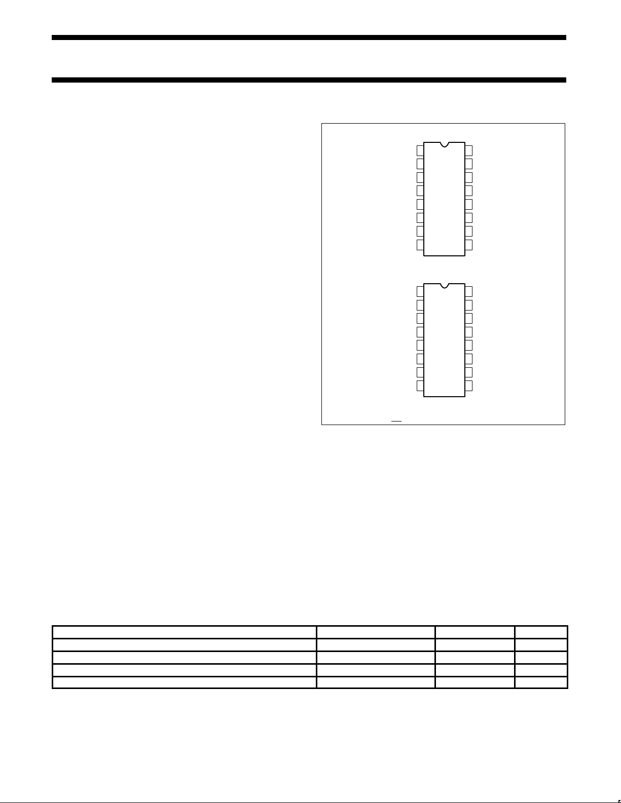
PIN CONFIGURATIONS
F, N Packages
D Package
1
NC
GND
V
EE
COMPEN
TOP VIEW
1
2
3
4
5
6
7
8
9
10
11
12
13
14
16
15
1
2
3
4
5
6
7
8
9
10
11
12
13
14
16
15
V
REF(–)
I
O
MSB A
1
A
2
A
3
A
4
V
REF(+)
V
CC
A8 LSB
A
7
A
6
A
5
A1 MSB
A
2
A
3
A
4
A8 LSB
A
7
A
6
A
5
V
REF(–)
V
REF(+)
COMPEN
NC
GND
V–
I
O
V+
NOTE:
1. SO and
non-standard pinouts.
ORDERING INFORMATION
DESCRIPTION TEMPERATURE RANGE ORDER CODE DWG #
16-Pin Ceramic Dual In-Line Package (CERDIP) -55 to +125°C MC1508-8F 0582B
16-Pin Ceramic Dual In-Line Package (CERDIP) 0 to +70°C MC1408-8F 0582B
16-Pin Plastic Dual In-Line Package (DIP) 0 to +70°C MC1408-8N 0406C
16-Pin Small Outline (SO) Package 0 to +70°C MC1408-8D 0005D

Philips Semiconductors Linear Products Product specification
MC1508-8/1408-88-bit multiplying D/A converter
August 31, 1994
738
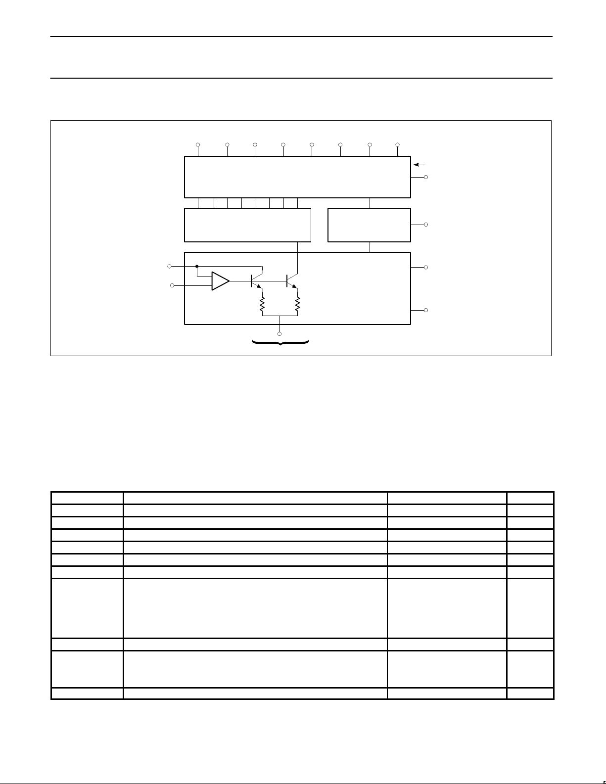
BLOCK DIAGRAM
CURRENT SWITCHES
5 6 7 8 9 10 11 12
MSB LSB
REFERENCE
CURRENT
AMPLIFIER
14
2
13
16
GND
COMPEN
NPN CURRENT SOURCE PAIR
A
1
A
2
A
3
A
4
A
5
A
6
A
7
A
8
4
BIAS
CURRENT
R-2R LADDER
15
(+)
(–)
V
REF
V
REF
V
CC
3
V
EE
I
O
CIRCUIT DESCRIPTION
The MC1508/MC1408 consists of a reference current amplifier, an
R-2R ladder, and 8 high-speed current switches. For many
applications, only a reference resistor and reference voltage need
be added.
The switches are non-inverting in operation; therefore, a high state
on the input turns on the specified output current component.
The switch uses current steering for high speed, and a termination
amplifier consisting of an active load gain stage with unity gain
feedback. The termination amplifier holds the parasitic capacitance
of the ladder at a constant voltage during switching, and provides a
low impedance termination of equal voltage for all legs of the ladder.
The R-2R ladder divides the reference amplifier current into
binarily-related components, which are fed to the remainder current
which is equal to the least significant bit. This current is shunted to
ground, and the maximum output current is 255/256 of the reference
amplifier current, or 1.992mA for a 2.0mA reference amplifier current
if the NPN current source pair is perfectly matched.
ABSOLUTE MAXIMUM RATINGS
SYMBOL PARAMETER RATING UNIT
V
CC
Positive power supply voltage +5.5 V
V
EE
Negative power supply voltage –16.5 V
V5 – V
12
Digital input voltage 0 to V
CC
V
V
O
Applied output voltage –5.2 to +18 V
I
14
Reference current 5.0 mA
V14, V
15
Reference amplifier inputs VEE to V
CC
P
D
Maximum power dissipation,
T
A
= 25°C (still-air)
1
F package 1190 mW
N package 1450 mW
D package 1080 mW
T
SOLD
Lead soldering temperature (10 sec) 300 °C
T
A
Operating temperature range 300 °C
MC1508 –55 to +125 °C
MC1408 0 to +75 °C
T
STG
Storage temperature range -65 to +150 °C
NOTES:
1. Derate above 25°C, at the following rates: F package at 9.5mW/°C; N package at 11.6mW/°C; D package at 8.6mW/°C
 Loading...