

Philips LX3600D-17, LX3600D-22, LX3600D-25, LX3600D-69, LX3600D-75 Service Manual
...
Service Manual
Service
Service
DVD Receiver
Service
Service
Service
LX3600D/17/22/25/69/75/78
©
Copyright 2003 Philips Consumer Electronics B.V. Eindhoven, The Netherlands
All rights reserved. No part of this publication may be reproduced, stored in a retrieval system or
transmitted, in any form or by any means, electronic, mechanical, photocopying, or otherwise
without the prior permission of Philips.
Published by KC 0327 Service Audio Printed in The Netherlands Subject to modification
Version 1.1
TABLE OF CONTENTS
Page
Location of pc boards & Version variations................1-2
Technical Specifications ............................................. 1-3
Measurement setup ....................................................1-4
Service Aids, Safety Instruction, etc. .........................1-5
Disassembly Instructions & Service positions ........... 2-1
Service Test Program .................................................3-1
Region code, Software version & upgrades...............3-2
Set Block diagram & Wiring diagram ............................ 4
PSU board (
Front Board .................................................................... 6
Mono AV Board .............................................................. 7
Amplifier Board .............................................................. 8
Speaker Connector Board ............................................. 9
Set Mechanical Exploded view & parts list ................. 10
History .......................................................................... 11
For info only
) .............................................. 5
CLASS 1
LASER PRODUCT
GB
3139 785 30371
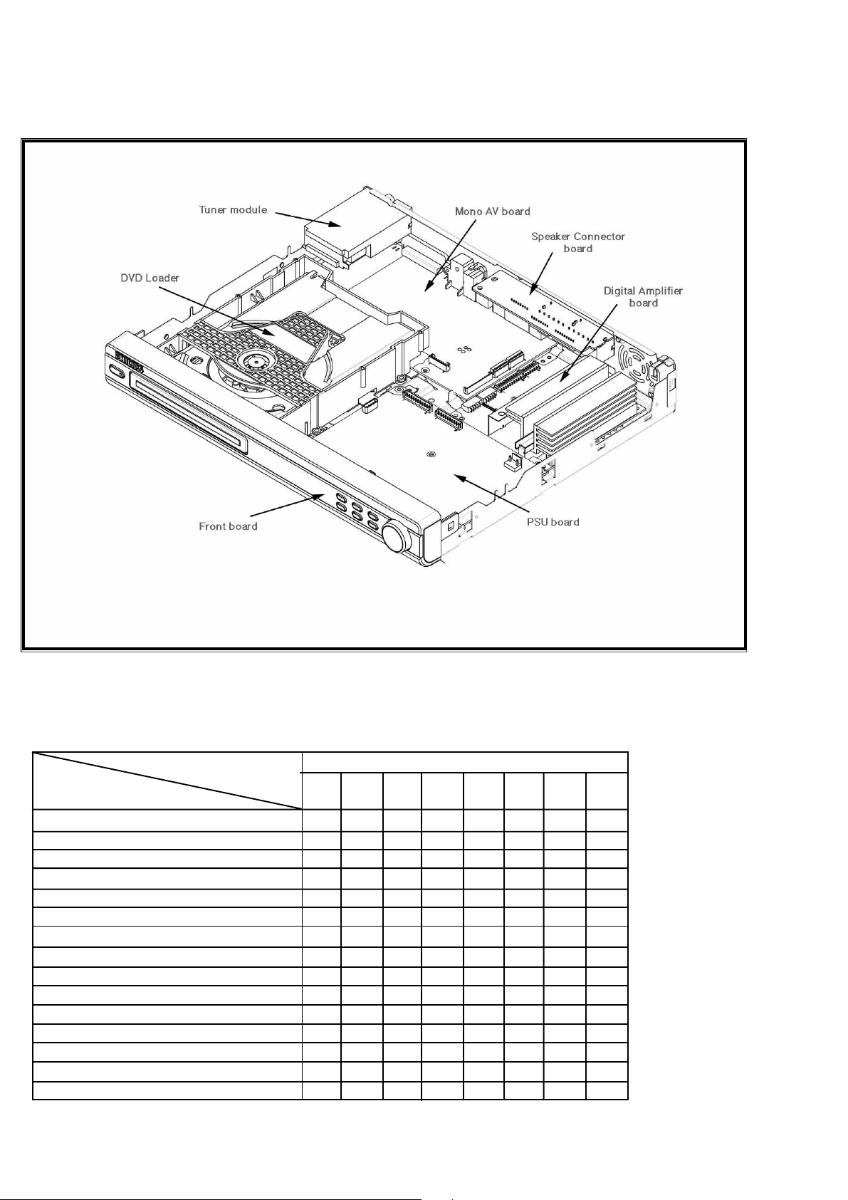
LOCATION OF PC BOARDS
1-2
VERSION VARIATIONS:
Type /Versions: LX3600D
Features &
/17 /22 /25 /69 /75 /78 /93
Board in used:
Progressive Scan x x
Voltage Selector x
1)
x
Aux-In xxxxxxx
TV-In x x x x x
Line-Out xxxxxxx
Composite (CVBS) Output x x x x x
S-Video Output xxxxxxx
Component (Pr/Y/Pb) Outputs x x x x x
SCART Output x x
1)
Production start-up with 220-240V PSU before changeover to PSU with voltage selector

SPECIFICATIONS
1-3
GENERAL:
Mains voltage : 120V for /17
220-240V for /22/25/75
110-127V/220-240V Switchable for /69/78
Mains frequency : 50/60Hz
Power consumption : < 2W at Standby
< 80W 1/8 P
rated
Dimension centre unit : 360 x 54 x 316mm
TUNER:
FM
Tuning range : 87.5-108MHz
Grid : 50kHz
IF frequency : 10.7MHz ± 25kHz
Aerial input : 75Ω coaxial
Sensitivity at 26dB S/N : < 7µV
Selectivity at 600kHz bandwidth : > 25dB
IF rejection : > 60dB
Image rejection : > 25dB
Distortion at RF=1mV, dev. 75kHz : < 3%
-3dB Limiting point : 8µV
Crosstalk at RF=1mV, dev. 40kHz : > 18dB
Output sensitivity
Line out : 700mV ± 2dB at 47kΩ
Scart-out : 600mV ± 2dB at 10kΩ
COMPACT DISC/VCD/DVD:
Video Decoding : MPEG-2 / MPEG-1
Video DAC : 8 Bits
Signal System : PAL / NTSC
Video Format : 4:3 / 16:9
MP3-CD bit rate
MP3-CD sampling frequencies
CBVS out
3)
4)
CVBS level : 1.0 ± 0.1V
: 32-256 kbs,variable bitrates
5)
: 32kHz, 44.1kHz, 48kHz
p-p
Luminance S/N ratio : > 55dB
YUV out
4)
Amplitude : 0.7V ± 0.1V
S/N ratio : > 60dB
S-Video out
4)
Y level : 1.0 ± 0.1V
p-p
Y S/N ratio : > 60dB
C level (burst) : 286mV
+1/-4 dB
p-p
MW
Tuning range : 531-1602kHz
530-1700kHz for /17/69
Grid : 9kHz
10kHz for /17/69
IF frequency : 450kHz ± 1kHz
Aerial input : Frame aerial
Sensitivity at 26dB S/N : < 4.0mV/M
Selectivity at 18kHz bandwidth : > 20dB
IF rejection : > 45dB
Image rejection : > 28dB
Distortion at RF=50mV, m=80% : < 5%
AMPLIFIER:
Stereo mode (DIN) : 2 x 50W RMS
Surround mode
2)
: 50W RMS/channel
1)
Frequency response ±3dB : 100Hz-20kHz
Hum (min, volume) : 200nW
Residue noise (min, volume) : 40nW
Input sensitivity
Aux-in : 900mV ± 3dB at 39kΩ
Scart-in : 500mV ± 3dB at 39kΩ
1)
with 4Ω, 1kHz & 10% THD
2)
with only channel(s) under meausrement loaded, all other
channels are unloaded.
3)
Recording format: ISO9660, UDF format is not supported.
4)
Output terminals terminated with 75Ω

MEASUREMENT SETUP
Tuner FM
1-4
Bandpass
LF Voltmeter
e.g. PM2534
RF Generator
e.g. PM5326
DUT
250Hz-15kHz
e.g. 7122 707 48001
Ri=50Ω
S/N and distortion meter
e.g. Sound Technology ST1700B
Use a bandpass filter to eliminate hum (50Hz, 100Hz) and disturbance from the pilottone (19kHz, 38kHz).
Tuner AM (MW,LW)
RF Generator
e.g. PM5326
Ri=50Ω
DUT
Frame aerial
e.g. 7122 707 89001
Bandpass
250Hz-15kHz
e.g. 7122 707 48001
LF Voltmeter
e.g. PM2534
S/N and distortion meter
e.g. Sound Technology ST1700B
To avoid atmospheric interference all AM-measurements have to be carried out in a Faraday´s cage.
Use a bandpass filter (or at least a high pass filter with 250Hz) to eliminate hum (50Hz, 100Hz).
CD
Use Audio Signal Disc
(replaces test disc 3)
DUT
L
R
SBC429 4822 397 30184
S/N and distortion meter
e.g. Sound Technology ST1700B
LEVEL METER
e.g. Sennheiser UPM550
with FF-filter
Recorder
Use Universal Test Cassette CrO2 SBC419 4822 397 30069
or Universal Test Cassette
LF Generator
e.g. PM5110
Fe SBC420 4822 397 30071
DUT
L
R
S/N and distortion meter
e.g. Sound Technology ST1700B
LEVEL METER
e.g. Sennheiser UPM550
with FF-filter

SERVICE AIDS
Service Tools:
Universal Torx driver holder .................................. 4822 395 91019
Torx bit T10 150mm ............................................. 4822 395 50456
Torx driver set T6 - T20 ......................................... 4822 395 50145
Torx driver T10 extended ...................................... 4822 395 50423
Compact Disc:
SBC426/426A Test disc 5 + 5A ............................ 4822 397 30096
SBC442 Audio Burn-in Test disc 1kHz ................. 4822 397 30155
SBC429 Audio Signals disc .................................. 4822 397 30184
Dolby Pro-logic Test Disc ...................................... 4822 395 10216
1-5
HANDLING CHIP COMPONENTS
1-6
GB
All ICs and many other semi-conductors are
susceptible to electrostatic discharges (ESD).
Careless handling during repair can reduce life
drastically.
When repairing, make sure that you are
connected with the same potential as the mass
of the set via a wrist wrap with resistance.
Keep components and tools also at this
potential.
Tous les IC et beaucoup d’autres
semi-conducteurs sont sensibles aux
décharges statiques (ESD).
Leur longévité pourrait être considérablement
écourtée par le fait qu’aucune précaution n’est
prise à leur manipulation.
Lors de réparations, s’assurer de bien être relié
au même potentiel que la masse de l’appareil et
enfiler le bracelet serti d’une résistance de
sécurité.
Veiller à ce que les composants ainsi que les
outils que l’on utilise soient également à ce
potentiel.
F
WARNING
ATTENTION
GB
Complete Kit ESD3 (small tablemat, wristband,
connection box, extention cable and earth cable) ...........4822 310 10671
Wristband tester ....................................................................4822 344 13999
ESD
D
WARNUNG
Alle ICs und viele andere Halbleiter sind
empfindlich gegenüber elektrostatischen
Entladungen (ESD).
Unsorgfältige Behandlung im Reparaturfall kan
die Lebensdauer drastisch reduzieren.
Veranlassen Sie, dass Sie im Reparaturfall über
ein Pulsarmband mit Widerstand verbunden
sind mit dem gleichen Potential wie die Masse
des Gerätes.
Bauteile und Hilfsmittel auch auf dieses gleiche
Potential halten.
ESD PROTECTION EQUIPMENT:
NL
Alle IC’s en vele andere halfgeleiders zijn
gevoelig voor electrostatische ontladingen (ESD).
Onzorgvuldig behandelen tijdens reparatie kan
de levensduur drastisch doen verminderen.
Zorg ervoor dat u tijdens reparatie via een
polsband met weerstand verbonden bent met
hetzelfde potentiaal als de massa van het
apparaat.
Houd componenten en hulpmiddelen ook op
ditzelfde potentiaal.
Tutti IC e parecchi semi-conduttori sono
sensibili alle scariche statiche (ESD).
La loro longevità potrebbe essere fortemente
ridatta in caso di non osservazione della più
grande cauzione alla loro manipolazione.
Durante le riparazioni occorre quindi essere
collegato allo stesso potenziale che quello della
massa dell’apparecchio tramite un braccialetto
a resistenza.
Assicurarsi che i componenti e anche gli utensili
con quali si lavora siano anche a questo
potenziale.
WAARSCHUWING
I
AVVERTIMENTO
GB
Safety regulations require that the set be restored to its original
condition and that parts which are identical with those specified,
be used
Safety components are marked by the symbol
!
.
NL
Veiligheidsbepalingen vereisen, dat het apparaat bij reparatie in
zijn oorspronkelijke toestand wordt teruggebracht en dat onderdelen,
identiek aan de gespecificeerde, worden toegepast.
De Veiligheidsonderdelen zijn aangeduid met het symbool
!
F
Les normes de sécurité exigent que l’appareil soit remis à l’état
d’origine et que soient utiliséés les piéces de rechange identiques
à celles spécifiées.
Less composants de sécurité sont marqués
!
D
Bei jeder Reparatur sind die geltenden Sicherheitsvorschriften zu
beachten. Der Original zustand des Geräts darf nicht verändert werden;
für Reparaturen sind Original-Ersatzteile zu verwenden.
Sicherheitsbauteile sind durch das Symbol
!
markiert.
I
Le norme di sicurezza esigono che l’apparecchio venga rimesso
nelle condizioni originali e che siano utilizzati i pezzi di ricambio
identici a quelli specificati.
Componenty di sicurezza sono marcati con
!
CLASS 1
LASER PRODUCT
GB
Invisible laser radiation when open.
Avoid direct exposure to beam.
Osynlig laserstrålning när apparaten är öppnad och spärren
är urkopplad. Betrakta ej strålen.
SF
Avatussa laitteessa ja suojalukituksen ohitettaessa olet alttiina
näkymättömälle laserisäteilylle. Älä katso säteeseen!
DK
Usynlig laserstråling ved åbning når sikkerhedsafbrydere er
ude af funktion. Undgå udsaettelse for stråling.
S
Warning !
Varning !
Varoitus !
Advarse !
GB
After servicing and before returning set to customer perform a leakage
current measurement test from all exposed metal parts to earth ground to
assure no shock hazard exist. The leakage current must not exceed
0.5mA.
F
"Pour votre sécurité, ces documents doivent être utilisés par
des spécialistes agréés, seuls habilités à réparer votre
appareil en panne".
DISMANTLING INSTRUCTIONS
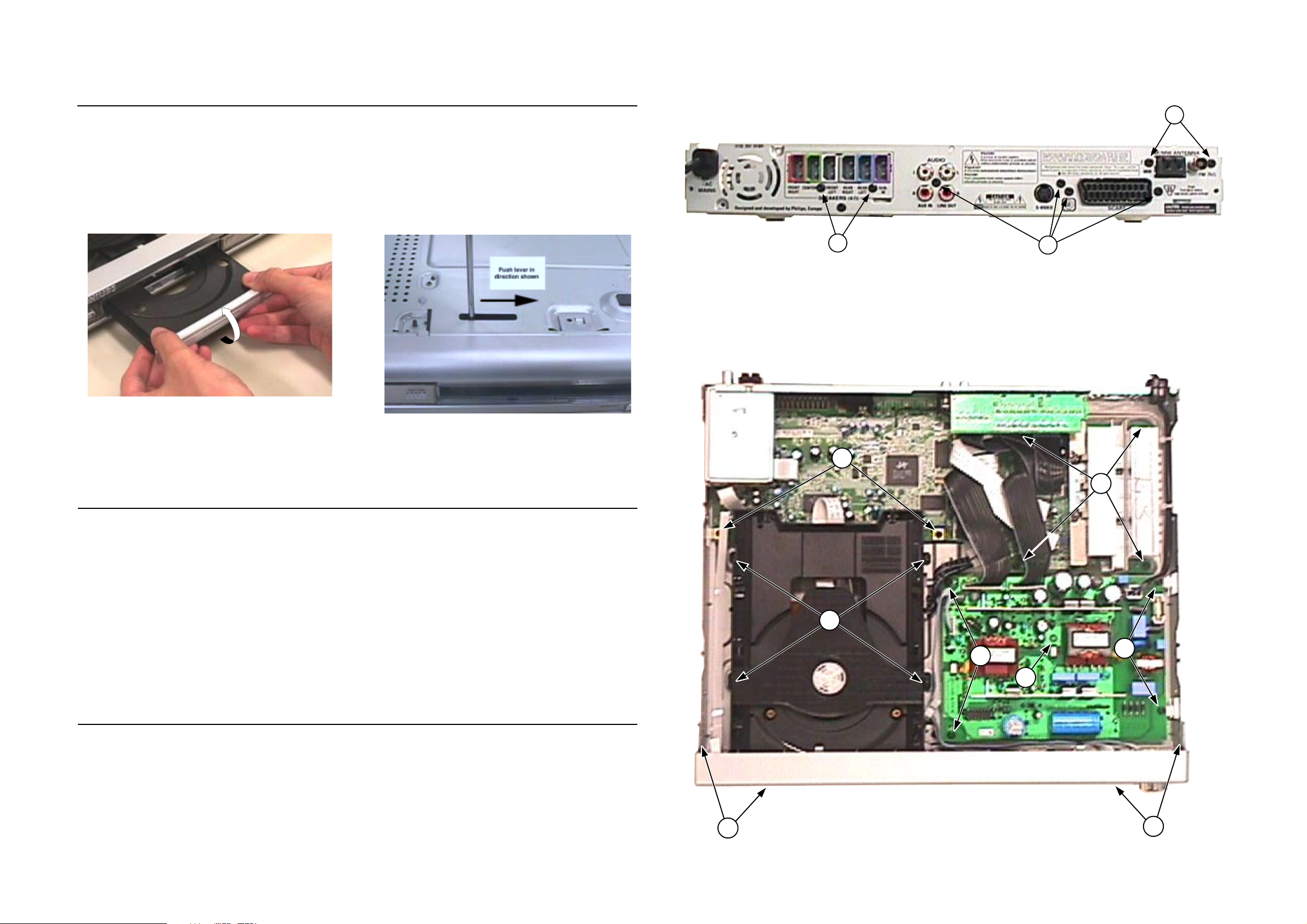
Dismantling of the Front Panel assembly
1) Open the Tray and remove the tray cover assy (pos 5 +
7) and remove it as shown in figure 1.
Note: The Tray can be manually open by inserting a
minus screw driver (approximately 9mm) and push
lever in the direction shown in figure 2.
2-1 2-1
2) Loosen the 5 screws to dismantle the Top Cover (pos
252)
- 2 screws on each side
- 3 screws on the Rear Panel (pos 251).
3) Uncatch 4 catches C2 (2x on side & 2x on the bottom) to
slide the Front Panel assembly (pos 101) as per figure 4.
A
Figure 1
Dismantling of the Tuner Module, Loader Mechanism & Mono AV board
1) Loosen 2 screws A to remove the Tuner Module (pos
1216) as per figure 3.
Figure 2
B
Figure 3
C
G
F
2) With the tray cover assembly (pos 5 + 7) already removed,
loosen 4 screws D to remove the Loader Mechanism
(pos 1210) as per figure 4.
3) Loosen 4 screws C on the rear and 2 screws G (see figure
3 and 4) to remove the Mono AV board (pos 1212).
Dismantling of the PSU, Speaker Connector and Amplifier boards
1) Loosen 4 screws E and 1 catch C1 to remove the PSU
board (pos 1215) as per figure 4.
2) Loosen 2 screws B to remove the Speaker Connector
board (pos 1211) as per figure 3.
3) Loosen 4 screws F to remove the Amplifier board (pos
1214) as per figure 4.
C2
D
Figure 4
E
E
C1
C2

Service positions
Mono AV board
2-2
2-2
Amplifier board
Thick insulation sheet or paper
Thick insulation sheet or paper
Speaker Connector board
Thick insulation sheet or paper

SERVICE TEST PROGRAM
To start service test program
hold S & SOURCE
buttons depressed and
press the STANDBY button*
* Mains power to set must be on
Hold till the Display is shown - ignore last setting info on the display
3-1
Display shows the
ROM version
"S-Vyy"
MAIN MENU
DISPLAY
TEST
BII
Button pressed?
Y
Display shows Figure 1
BII
Button pressed?
Y
S refers to Service Mode
V refers to Version
yy refers to Software version number of the uProcessor
(counting up from 01 to 99)
N
Figure 1
N
Figure 2
Display shows Figure 2
9
Button pressed?
Y
TEST
TEST
ROTARY
ENCODER TEST
LEAVE SERVICE
TEST PROGRAM
N
Various
other Tests
Activated with
SEEPROM FORMAT
SOURCE / VOLUME
Knob
Disconnect
mains cord
ACTION
Load default data. Display shows "NEW" for 1 second.
Caution!
All presets from the customer will be lost!!
Display shows value for 2 seconds.
Values increases or decreases in steps of 1 until
0 (Min.) or 40 (Max.) is reached.
LX3600D Service Test Program dd wk0326

3-2
Procedure to change Tuner Grid (not for /00/25/17)
During the standby mode, hold the SOURCE and PLAY
buttons down and press the STANDBY button.
The display will show the new tuning grid "GRID 9" or
"GRID 10".
Note: Repeating the same action will toggle back to its
previous tuning grid setting.
Reprogramming of DVD version Matrix *
After repair of the Mono AV board the customer setting
and region code may be lost.
Reprogramming will put the set back in the state in which
it has left the factory, ie. with the default setting and the
allowed region code.
To reprogram do as follows:
1) Put the set in Stop mode with tray open
2) Press the following buttons on the Remote Control:
<9> <9> <9> <9> <AUDIO> <8> ........... for LX3600D/17
<9> <9> <9> <9> <AUDIO> <1> ........... for LX3600D/22
<9> <9> <9> <9> <AUDIO> <1> ........... for LX3600D/25
<9> <9> <9> <9> <AUDIO> <3> ........... for LX3600D/69
<9> <9> <9> <9> <AUDIO> <4> ........... for LX3600D/75
<9> <9> <9> <9> <AUDIO> <6> ........... for LX3600D/78
<9> <9> <9> <9> <AUDIO> <2> ........... for LX3600D/93
<9> <9> <9> <9> <AUDIO> <5> .. for LX3600D India Kit
<9> <9> <9> <9> <AUDIO> <7> . for LX3600D Brazil Kit
<9> <9> <9> <9> <AUDIO> <1> ............ for MRD260/22
* Note: Applicable for software version 27 onwards. For
lower versions the set must be upgraded first
before the DVD version matrix is applicable.
Procedure for check Software version
1) Power up the set and open tray in DVD mode.
2) Press OSD button on the Remote control.
3) The TV screen will shows:
SERVO:nnnnnnnn REG:r
MMMMMMM-yymmdd-Vxx SSS
where
nnnnnnnn = servo version number
r = region number
MMMMMMM = LX3600D or MRD260
yymmdd = software date in year, month, day format
xx = version number
SSS = stroke version eg. /00 or /05, etc.
Procedure to upgrade software
1) Power up the set and open tray in DVD mode.
2) Place upgrade CD-ROM onto tray and close.
3) The set will response and display the following:
- LOAD [After the disc is read, the tray will open for you
to remove the disc]
- ERASE 0 -> ERASE F ...... -> ERASE 0
- WRITE F ...... -> WRITE 0
- UPG END [only for a short moment, if unsuccessful
ERROR is displayed]
- DISC
- LOAD [Tray will close indicating that the upgrade
process is completed]
4) Unplug the set to disconnect the mains supply.
5) The whole process should last for about 5 minutes.
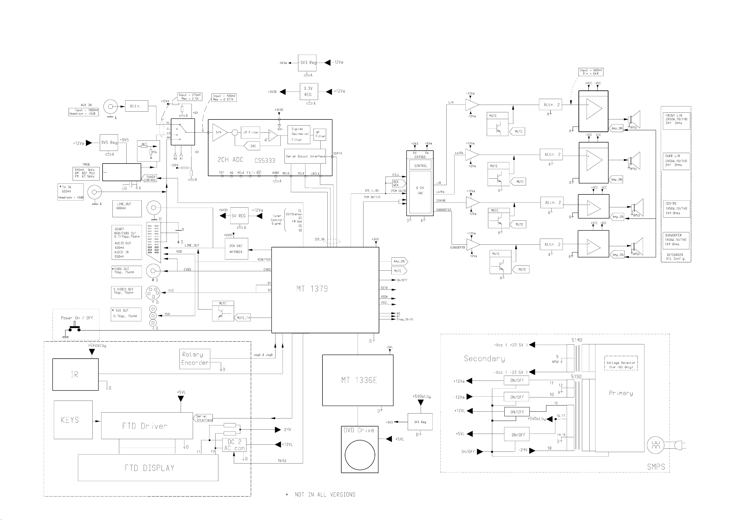
SET BLOCK DIAGRAM
4-1 4-1
TDA8920
TUNER
(TM 08)
74HC4052
L/R
POWER AMP
TDA8920
SURROUND
POWER AMP
1/2xTDA8920
1/2XTDA8920
LX3600D/22 Block Diagram ....37121 dd wk334.5

WIRING DIAGRAM
4-2
4-2
FE
1
EH 5P
340mm
3139 110 38821
1
1
EH 10P
140mm
10
1
5
EH 11P
120mm
3139 111 01751
11
24
PH 9P
120mm
3139 110 28081
FFC, 0.5mm pitch
24p
1
1
BD
8P
480mm
3139 110 35391
AD 4P
280mm
3139 110 34581
1
1
EH
100mm
9P
1
EH
8p 100mm
1
EH
8p 100mm
1
1
10P
1
1
1
10P
AD
140mm
AD
140mm
1
1
1
220mm
1p
24
1
1
1
1
FFC BD 11p
100mm
3139 110 35910
1
LX3600D/22 Set Wiring ...37110 dd wk334.5

5-1
PSU BOARD
(For Information only)
It is not recommended for component repair on this board but
to replace the board when it becomes defective.
Therefore no service parts list is published in this chapter.
The only service part available for replacement is:
PSU Board 220V-240V ...................................... 3122 429 00191
PSU Board Voltage Selector ........................... 3122 429 00241
PSU Board 120V ............................................... 3122 429 00261
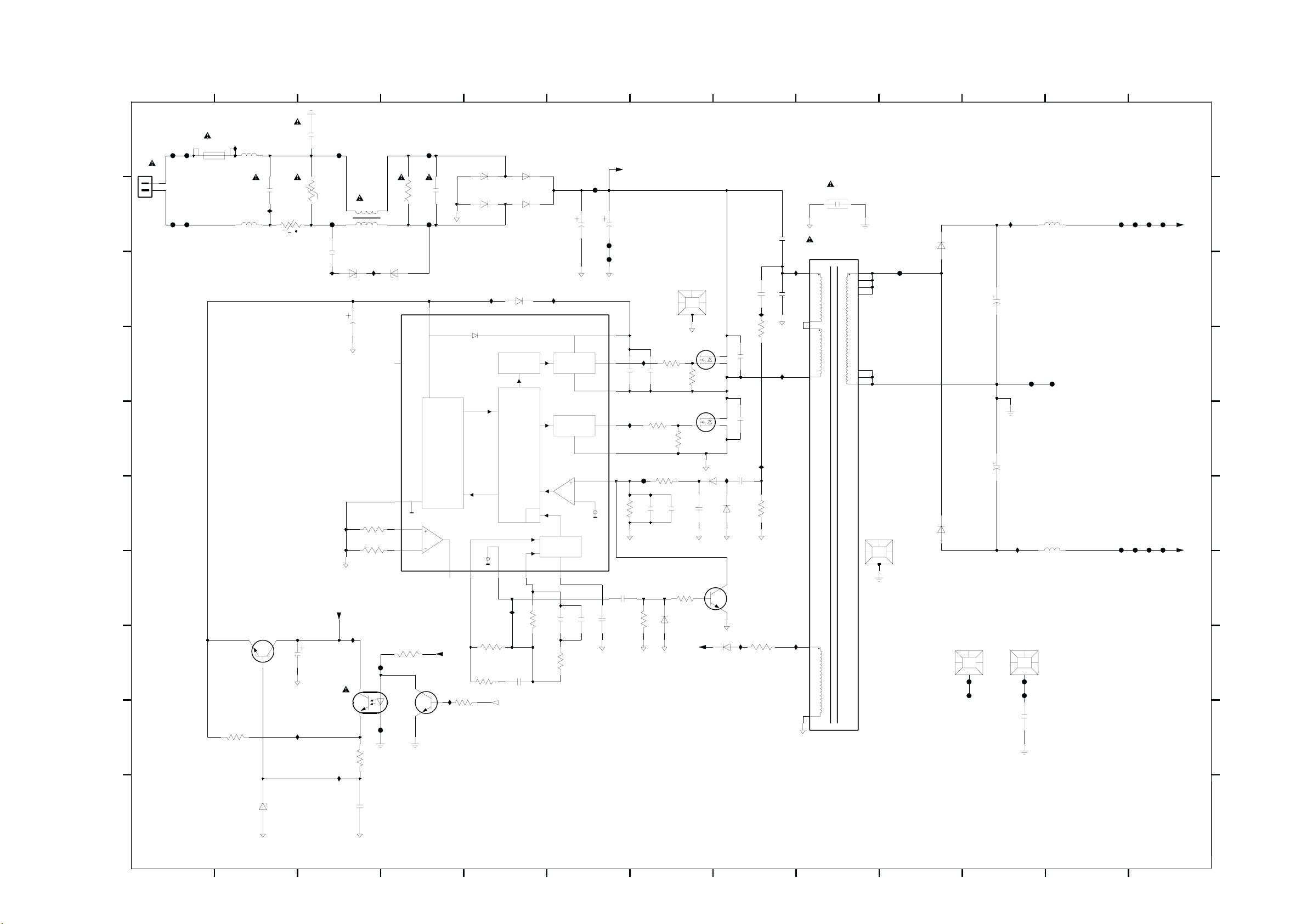
5-2
5-2
PSU CIRCUIT 1 - 220-240V version
A
B
B2P-VA-BF
2
1
1100
F102F101
F103 F104
1101
VALUE
I130
5100
90Mhz 700R
5101
90Mhz 700R
(FOR INFORMATION ONLY)
2100
220n
I131
3100
B57236
C
D
E
F
G
7153
BC547B
H
I
3153
2K2
t
22u
I129
AMP
2101
470p
V
3101
SIOV-S14K300S11M5
F107
2117
33n
I101
Vaux
2153
7119
TCET1102
I128
HF2430
5103
I102
2
6102
PDZ-13B
1
43
6101
PDZ-13B
7120
3105
10u
2103
NC
5
SGND
9
3127
I+ 2
100K
3128
1I-
100K
I127
3204
2K2
F213
7202
BC847B
F214
DD
2K2
3154
F106F105
2106
680K
F108
VDD
11
SUPPLY
GM
ERROR
AMPLIFIER
6105
220n
6107
TEA1610
BOOTSTRAP DIODE
3V
14
3
IRS
VCO
+12V
3171
3203
1K0
15K
I134
6106
1N40061N4006
6108
1N40061N4006
I111
6128
PG106R
LEVEL
SHIFTER DRIVER
LOGIC
+2
+
16
VREF
I119
0.6V
12
IFS
3170
3169
36K
2166
220n
Inv_stby
I110
HIGH SIDE
LOW SIDE
DRIVER
OSCILLATOR
13
CF
3K9
2105
3177
2108
470n
2K7
2.33V
2168
654321
7
1312111098
A
+VB
F109
2140
47u
2165
470n
2112
7
6
10
4
15
+
100u
F110
F111
FVDD8
GH
SH
GL
PGND
SD
2169
150n
180p
2167
I132
3164
I109
470n
F115
33K
3178
2160
3162
2170
220K
470n
10R
3165
10K
470n
6154
3160
10R
2171
MECHPART
0100
7121
STP6NK60ZFP
3161
7122
STP6NK60ZFP
3163
470K
2163
470n
3179
100K
BAS316
Vaux
470K
6160
BAS316
10n
2114
I104
3102
330p
2161
2162
330p
I116
6161
6126
BAV21
I117
2164
10n
3166
BAS316
7154
BC847B
I123 I124
3176
22R
1n0
100R
2113
2115
100R
I105
100n100n
I103
5
5140
CQ32
1
2
3
4
1n
AMP
6200
F222
STPS8H100FP
10
9
0200
MECHPART
6201
STPS8H100FP
AMP
0206
HOLE
2202
2203
I201
3m3
AMP
3m3
I202
0207
HOLE
F224
5200
10u
F225
5201
10u
F205
F207F206
F208
+VCC
B
C
D
E
F
F211F209 F210
F212
-VCC
G
H
2208
F203
F204
33n
F218
F219
6
I
AMP
10n
6153
J
PDZ-13B
1
2154
65432 1312111098
7
3122 427 23680
J
2003-06-11

5-3 5-3
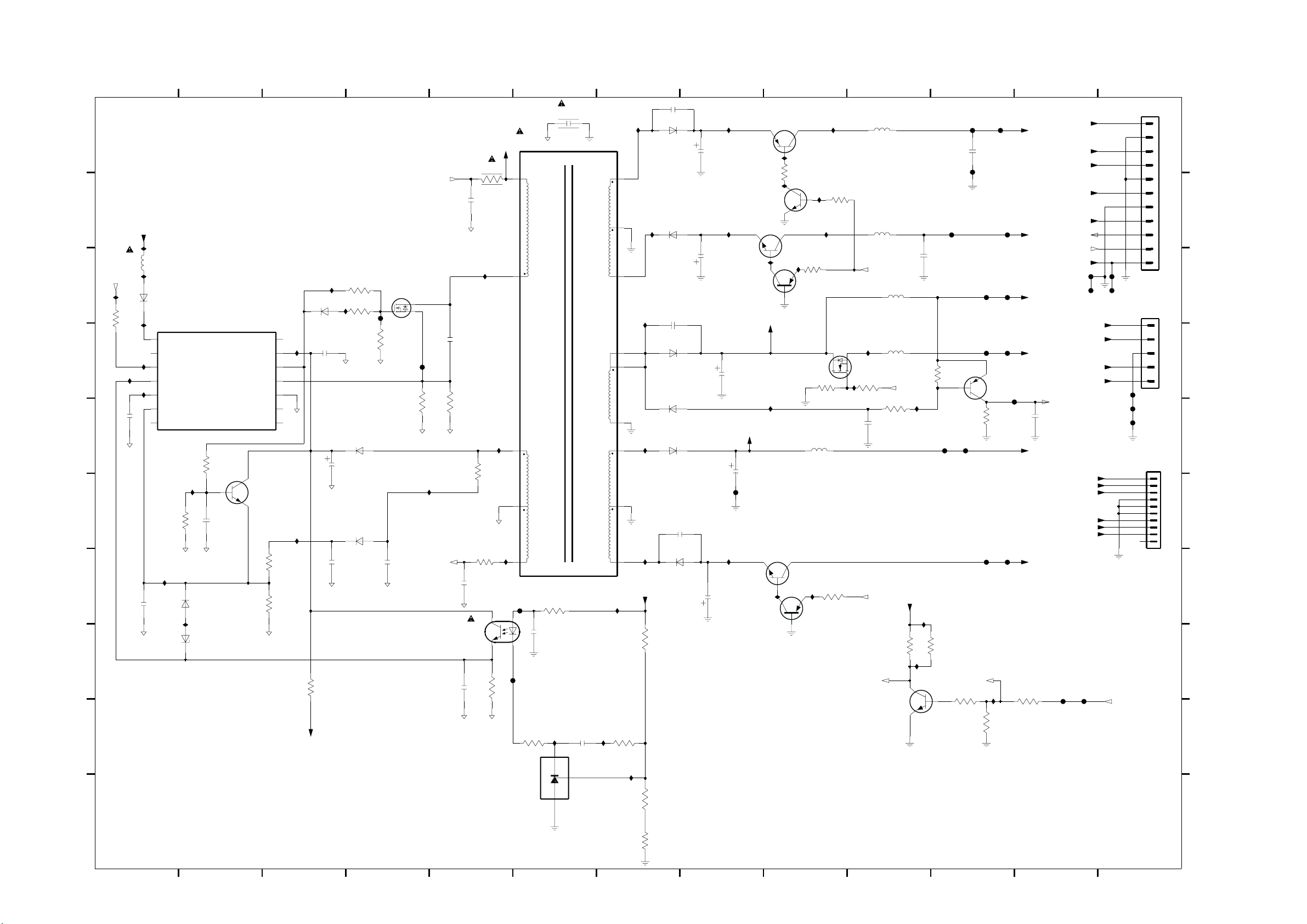
PSU CIRCUIT 2 - 220-240V version
(FOR INFORMATION ONLY)
A
B
HV
I169
2u2
5130
DEMAG
C
D
I161
3131
22K
I159
2130
I157
6135
I153
I158
I160
1n
1N4006
7130
TY72011AP2
1
HV
2
NC1
3
DEMAG
4
FB
5
CT
6
OVP
7
NC2
NC5
VCC
DRIVE
ISENSE
GND
NC4
NC3
14
13
12
11
10
9
8
E
3140
100K
I154
7140
BC847B
F
220n
2141
3141
100K
22K
I163
3133
G
3132
5K6
H
2133
22n
6133
I164
6132
BAS316
BZX79-C6V2
I
I155
I168
3138
Vaux
I152
6125
1N4148
100n
2138
2131
2132
5K6
I156
22u
100n
3106
330R
3126
33R
6131
BAV21
6130
BAV21
STP3NK60ZFP
F126
47K
3125
2136
7125
100p
+VB
2120
F125
1R
31211R3122
I167
DEMAG
TCET1102
220p
2135
2139
3137
7190
68p
22n
I150
3135
2K2
3123
1R
1K5
3139
I166
HV
I165
4K7
5190
CT282D4
2
5
9
8
7
F294
F295
2295
D
3293
220R
22n
654321
3295
22R
I268
1
2190
1n
D
2292
220n
7290
TL431CZ
3
7
2220
470p
I250 I251
11
12
A
10
16
17
15
D
13
14
D
18
I279
3292
220R
I272
6220
BYV27-200
I256 I257
6280
PG106R
I261
2254
180p
6253
SB360
6254
1N4148
I263
6210
PG106R
2241
3297
470p
6240
1N4006
5K1
I267
Vreg1
2221
2280
2240
1312111098
BC327-25
3282
8K2
SI2302DS
7250
D
5210
10u
3242
10K
I252
3221
10K
I258
3250
100K
7220
470u
A
100u
A
D
2250
D
22u
BC857B
1m
+12V
2210
F217
D
I269
7282
220u
7242
BC857B
7221
BC847B
I259
Vreg1
I275
I271
I253
2K2
3201
I254
A
7280
BC337-40
I260
A
7240
BC337-40
D
Not_STBY
I265
I264
10K
3251
2252
Not_STBY
Not_STBY
5220
10u
5280
10u
100n
D
BC847B
5251
6u8
5250
6u8
Not_STBY
3252
68K
+12V
7255
3254
I266
I274
2282
A
I280
2K2
3258
22n
3259
F215
F280
1K5
2K2
F220
2222
F223
F216
Inv_stby
3255
1K
A
F250
F240
3257
F221
22n
F281
F231F230
F251
BC857B
7252
2K7
3253
2253
DD
F241
I278
56K
F232
3256
0u47
10K
+12VA
-12VA
+5VDstby
+5VL
100n
2255
D
+12VL
-24V
F292
+5VDstby
+5VDstby
+5VL
+12VA
-12VA
STBY
Power_down
+12V
F270
F271
+12VL
+5VDstby
Power_down
+VCC
+VCC
+VCC
-VCC
-VCC
-VCC
F293
+5VL
-24V
F276
A
F277
F272
F273
F274
AMP
STBY
A
0201
EH-B
1
2
B
3
4
5
6
7
8
9
10
11
C
D
0202
EH-B
1
2
3
4
5
D
0203
EH-B
D
E
1
2
3
4
5
6
F
7
8
9
10
G
H
I
DD
7
3291
3290
D
3K9
1K2
3122 427 23680
J
2003-06-11
2
J
D
1
65432 1312111098

5-4 5-4
PSU CIRCUIT 1 - Voltage Selector version
(FOR INFORMATION ONLY)
AMP
A
B
B2P-VA-BF
2
1
1100
F101
F103
F102
F104
1101
VALUE
I130
5100
90Mhz 700R
5101
90Mhz 700R
2100
I131
220n
3100
B57236
470p
2101
F105
V
3101
F107
t
HF2430
12
SIOV-S14K300S11M5
43
2117
6101
33n
I101
PDZ-13B
C
2103
D
E
F
G
Vaux
H
7153
BC547B
22u
2153
I
3153
2K2
I129
7119
TCET1102
I128
I127
2K2
654321
F106
2112
2108
2.33V
2168
330u
F110
F111
I126
2165
470n
330u
10
15
+
F120
7
6
4
+VB
3103
3107
FVDD8
GH
SH
GL
PGND
SD
180p
680K
680K
2167
I132
3164
2169
150n
6105 6106
1N4006
3105
2106
220n
680K
F108
5103
I102 I103
6102
PDZ-13B
7120
VDD
5
9
1I-
3204
2K2
7202
11
SUPPLY
GM
ERROR
AMPLIFIER
10u
3127
100K
3128
100K
NC
SGND
I136
I137
F213
F214
I+ 2
BC847B
1N4006
F119
F112
TEA1610
BOOTSTRAP DIODE
3V
3
14
VCO
IRS
I108
+12V
3171
3203
1K0
15K
I134
3169
1N4006
61086107
1N4006
1102
2
5
SDKG
I111
6128
PG106R
LEVEL
SHIFTER DRIVER
LOGIC
+2
+
16
VREF
I119
0.6V
12
IFS
3170
36K
I125
2166
220n
Inv_stby
1
F113
F121
3
4
6
I110
HIGH SIDE
LOW SIDE
OSCILLATOR
I135
3K9
2105
3177
DRIVER
13
CF
470n
I122
2K7
F109
I109
470n
F115
33K
3178
2160
3162
2170
10R
I121
220K
3160
470n
3165
10K
470n
6154
7
MECHPART
0207
10R
I107
3163
470n
2171
3179
100K
BAS316
Vaux
7121
STP6NK60ZFP
I106
3161
470K
7122
STP6NK60ZFP
470K
I120
6160
BAS316
10n
2163
I116
6161
6126
BAV21
21612162
2164
10n
BAS316
7154
BC847B
330p
330p
2114
I104
3102
I117
3166
3176
22R
1n0
100R
39R
DD
3154
2115 2113
I105
1312111098
A
2140
22n
22n
5140
CT283D3
1
1n
AMP
6200
16
15
F222
STPS8H100FP
2202
I201
3m3
5200
10u
F206 F207F205
F208
+VCC
B
C
2
3
4
14
13
F224
F225
D
AMP
E
3m3
2203
F
6201
0200
STPS8H100FP
I202
MECHPART
5201
10u
F211
F210F209
F212
-VCC
G
AMP
I124I123
5
0206
HOLE
0207
HOLE
H
2143
F203
F204
33n
7
6
F218
F219
I
AMP
6153
J
PDZ-13B
10n
2154
J
Cheetah 10 Doubler - WR HB Converter 3122 427 23770 dd 2003-08-21
1
65432 1312111098
7
5-5
5-5
PSU CIRCUIT 2 - Voltage Selector version
(FOR INFORMATION ONLY)
A
B
HV
I169
2u2
5130
DEMAG
C
D
I161
3131
22K
I159
2130
I157
6135
I153
I158
I160
1n
1N4006
7130
TY72011AP2
1
HV
2
NC1
3
DEMAG
4
FB
5
CT
6
OVP
7
NC2
NC5
VCC
DRIVE
ISENSE
GND
NC4
NC3
6125
1N4148
14
I155
13
12
11
10
9
8
100n
2138
E
3140
100K
I154
7140
BC847B
F
2141
100K
220n
3133
I168
22K
3141
I163
G
3132
5K6
3138
Vaux
5K6
H
22n
2133
6133
I164
6132
BAS316
BZX79-C6V2
I
I152
2131
2132
I156
22u
100n
3106
330R
3126
33R
6131
BAV21
6130
BAV21
STP3NK60ZFP
F126
47K
3125
2136
7125
100p
+VB
2120
F125
31211R3122
I167
DEMAG
TCET1102
220p
1R
2135
2139
2125
7190
I150
3137
3135
2K2
68p
22n
3123
33n
1K5
3139
1R
I166
HV
I165
4K7
5190
CT282D4
2
5
9
8
7
F294
F295
2295
D
3293
220R
22n
654321
3295
22R
I268
1
2190
1n
D
2292
220n
7290
TL431CZ
3
I270
I279
11
12
10
16
17
15
13
14
18
3292
220R
I272
A
D
D
7
I261
I263
Vreg1
3297
2220
470p
6220
BYV27-200
6280
PG106R
2254
180p
6253
SB360
6254
1N4148
6210
PG106R
2241
470p
6240
1N4006
5K1
I251 I252I250
2221
470u
A
I257 I258I256
2280
100u
A
2240
D
BC857B
1m
2250
DD
+12V
2210
F217
D
I269I267
22u
7282
220u
7242
BC857B
7221
BC847B
I259
Vreg1
I275
I271
7220
I253I254
2K2
3201
A
7280
BC337-40
I260
A
7240
BC337-40
D
BC327-25
3282
SI2302DS
8K2
I113
I112
7250
5210
10u
3250
100K
3242
10K
3221
10K
Not_STBY
I265
I264
10K
3251
2252
Not_STBY
Not_STBY
5220
10u
5280
10u
100n
D
BC847B
5251
6u8
5250
6u8
Not_STBY
3252
68K
7255
+12V
3254
F280 F281
22n
2282
A
3259
I266
F215
I280
2K2
2K2
3258
I274
1K5
F220
2222
F223
A
F216
Inv_stby
3255
1K
F221
22n
F231
F230
F250 F251
BC857B
7252
2K7
3253
D
F241
F240
I278
56K
3257
D
F232
+12VA
-12VA
+5VDstby
+5VL
2255
+12VL
-24V
3256
10K
+5VDstby
+5VDstby
Power_down
Power_down
100n
D
F292
+5VL
+12VA
-12VA
STBY
+12V
F270
F271
+5VL
+12VL
+5VDstby
+VCC
+VCC
+VCC
-VCC
-VCC
-VCC
F293
-24V
A
F276
F277
F272
F273
F274
AMP
D
STBY
1312111098
1
2
A
3
4
5
0201
EH-B
6
7
B
8
9
10
11
C
0202
EH-B
1
2
3
4
5
D
0203
EH-B
D
E
1
2
3
4
5
6
F
7
8
9
10
G
H
I
7
3290 3291
3K9
J
1K2
D
Cheetah 10 Doubler - WR FB Converter 3122 427 23770 dd 2003-08-21
2
J
D
1
65432 1312111098

5-6
5-6
PSU CIRCUIT 1 - 120V version
A
B
B2P-VA-BF
2
1
1100
F103
F102F101
F104
1101
VALUE
I130
5100
90Mhz 700R
5101
90Mhz 700R
(FOR INFORMATION ONLY)
2100
220n
I131
3100
t
B57236
C
D
E
F
G
7153
BC547B
H
I
3153
2K2
22u
I129
AMP
470p
2101
F105
V
3101
SIOV-S14K300S11M5
F107
Vaux
2153
7119
TCET1102
I128
HF2430
1
43
1103
DSP
5103
I102
2
3104
220R
7120
10u
2103
NC
5
SGND
9
I136
3105
I127
2K2
3127
100K
3128
100K
I+ 2
I137
1I-
AMPLIFIER
3204
2K2
F213
7202
BC847B
F214
DD
3154
F106
680K
F108
ERROR
2106
GM
220n
TEA1610
VDD
11
BOOTSTRAP DIODE
SUPPLY
3
VCO
I108
+12V
I134
3203
1K0
F119
6105
6107
1N4006
F112
3V
14
IRS
3169
3171
15K
6106
1N40061N4006
6108
1N4006
9108
6128
PG106R
LEVEL
SHIFTER DRIVER
LOGIC
+2
+
16
VREF
I119
0.6V
12
IFS
3170
36K
I125
2166
220n
Inv_stby
F113
F121
I110I111
HIGH SIDE
LOW SIDE
DRIVER
OSCILLATOR
13
CF
I135
3K9
2105
3177
470n
I122
2K7
2112
2108
2.33V
2168
654321
F110
F111
I126
470n
330u
330u
10
15
+
2165
F120
7
6
4
+VB
3103
3107
FVDD8
GH
SH
GL
PGND
SD
180p
2169
150n
680K
680K
2167
I132
3164
F109
I109
470n
F115
33K
3178
2160
3162
2170
470n
10R
I121
220K
3165
10K
470n
6154
7
3160
10R
2171
MECHPART
0204
7121
STP6NK60ZFP
I106
3161
7122
STP6NK60ZFP
I107
3163
470K
I120
2163
470n
3179
100K
BAS316
Vaux
470K
6160
BAS316
10n
I116
6161
6126
BAV21
2161
2162
2164
10n
BAS316
7154
BC847B
I123
330p
330p
2114
I104
3102
I117
3166
3176
22R
1n0
39R
2113
2115
100R
I105
I124
I103
22n22n
5140
CT283D3
1
2
3
4
5
7
6
2140
1n
AMP
16
15
14
13
6200
6201
0206
HOLE
F222
0200
STPS8H100FP
2202
F224
F225
2203
STPS8H100FP
AMP
F218
F219
I201
3m3
AMP
3m3
I202
MECHPART
0207
HOLE
2143
AMP
F203
F204
33n
5200
10u
5201
10u
F205
1312111098
A
+VCC
B
F208
F207F206
C
D
E
F
F212
F211F209 F210
-VCC
G
H
I
10n
6153
J
PDZ-13B
2154
J
Cheetah 10 Doubler - USA HB Converter 3122 427 23810 dd 2003-09-17
1
65432 1312111098
7

5-7
5-7
PSU CIRCUIT 2 - 120V version
(FOR INFORMATION ONLY)
A
B
HV
I169
2u2
5130
DEMAG
I161
3131
22K
I159
2130
I157
6135
I153
I158
I160
1n
1N4006
7130
TY72011AP2
1
HV
2
NC1
3
DEMAG
4
FB
5
CT
6
OVP
7
NC2
NC5
VCC
DRIVE
ISENSE
GND
NC4
NC3
C
D
E
3140
100K
I154
7140
BC847B
F
220n
2141
3141
100K
I163
3133
G
H
2133
22n
6133
I164
6132
BAS316
BZX79-C6V2
3132
I
14
13
12
11
10
9
8
22K
5K6
I155
I168
3138
Vaux
I152
6125
1N4148
100n
2138
2131
2132
5K6
I156
22u
100n
3106
330R
3126
33R
6131
BAV21
6130
BAV21
STP3NK60ZFP
F126
47K
3125
2136
7125
100p
F125
3121
I167
DEMAG
+VB
1R
2125
220p
2120
1R
3122
2135
TCET1102
2139
3137
68p
7190
22n
33n
I150
3135
2K2
3123
1R
1K5
3139
I166
HV
I165
4K7
5190
CT282D4
2
5
9
8
7
F294
F295
2295
D
3293
220R
22n
654321
3295
22R
I268
1
2190
1n
2292
220n
7290
TL431CZ
3
A
F276
F277
F272
F273
F274
AMP
STBY
1312111098
1
2
A
3
4
5
0201
EH-B
6
7
B
8
9
10
11
D
0202
EH-B
1
2
3
4
5
D
0203
EH-B
C
D
E
1
2
3
4
5
6
F
7
8
9
10
G
H
I
7
2220
I250 I251
D
11
12
A
10
16
17
15
D
13
14
D
18
I279
I270
3292
220R
I272
470p
6220
BYV27-200
2221
A
I256 I257
6280
PG106R
2280
A
I261
2254
180p
6253
SB360
6254
1N4148
I263
6210
PG106R
2241
470p
6240
1N4006
Vreg1
5K1
2240
D
470u
100u
2250
D
22u
I269I267
1m
2210
F217
D
7282
BC857B
+12V
220u
7242
BC857B
BC847B
I259
Vreg1
I275
7221
I271
7220
I253
3201
I254
2K2
A
7280
BC337-40
I260
A
7240
BC337-40
D
BC327-25
I112
3282
8K2
SI2302DS
7250
D
5210
10u
I113
I258
3250
100K
I252
3242
10K
3221
10K
Not_STBY
I265
I264
10K
3251
2252D100n
Not_STBY
Not_STBY
5220
10u
5280
10u
2282
A
5251
6u8
5250
6u8
Not_STBY
I266
3252
68K
+12V
I280
2K2
3258
3254
I274
7255
BC847B
DD
22n
3259
F215
2K2
F220 F221
2222
F223
A
F230
1K5
F216
F240 F241
Inv_stby
3255
1K
3257
22n
BC857B
7252
3253
I278
F281F280
F231
F251F250
F232
2K7
D
3256
10K
56K
+12VA
-12VA
Power_down
+5VDstby
+5VL
100n
2255
D
+12VL
-24V
+5VDstby
+5VDstby
+5VL
+12VA
-12VA
STBY
+12V
F270
F271
+12VL
+5VDstby
Power_down
+VCC
+VCC
+VCC
-VCC
-VCC
-VCC
F293
F292
+5VL
-24V
2
J
D
1
65432 1312111098
3K9
3291 3297
J
1K2
3290
D
Cheetah 10 Doubler - USA FB Converter 3122 427 23810 dd 2003-09-17
7

6-1
6-1
FTD DISPLAY PIN CONNECTIONS
FRONT BOARDS
TABLE OF CONTENTS
7G
f
e
6G
a
h
g
r
(1G-7G)
5G 4G 3G 2G 1G
j
s
p
d
b
k
m
n
c
Col
FTD Display pin connection ......................................................................... 6-1
Front Standby part - circuit & layouts ........................................................... 6-2
Front Display part - Circuit diagram ............................................................. 6-3
Front Display part - Component & Chip layouts .......................................... 6-4
Front Display part - Chip layout Part A......................................................... 6-5
Front Display part - Chip layout Part B ........................................................ 6-6
Electrical parts list......................................................................................... 6-7
P1
P2
P3
P4
P5
P6
P7
P8
P9
P10
P11
P12
P13
P14
7G
a
j , p
h
k
b
m
g
c
e
n
d
6G
a
j , p
h
k
b
f
r
-
f
m
g
c
e
r
n
d
-
5G
a
j , p
h
k
b
f
m
g
c
e
r
n
d
col
4G
a
j , p
h
k
b
f
m
g
c
e
r
n
d
-
3G
a
j , p
h
k
b
f
m
g
c
e
r
n
d
col
2G
a
j , p
h
k
b
f
m
g
c
e
r
n
d
-
1G
a
j , p
h
k
b
f
m
g
c
e
r
n
d
-
P15
FTD DISPLAY PIN NO.
FUNCTION
s
12
s
1
14
1
1
8
9
7
P
N
P
15
C
1
1
5
6
P
P
13
2
2
2
2
2
2
3
3
2
2
2
2
0
1
N
N
N
C
C
C
2
4
6
7
8
3
5
6
7
G
4
5
G
G
G
9
3
2
1
G
G
G
3
0
1
2
N
F
F
P
2
2
s
s
2
1
F
F
2
1
s
6
5
4
3
P
P
P
N
P
3
2
1
s
7
1
8
9
0
P
P
P
P
4
7
5
6
s
1
1
1
1
P
8
1
2
3
4
P
P
P
9
10
11
6-2 6-2
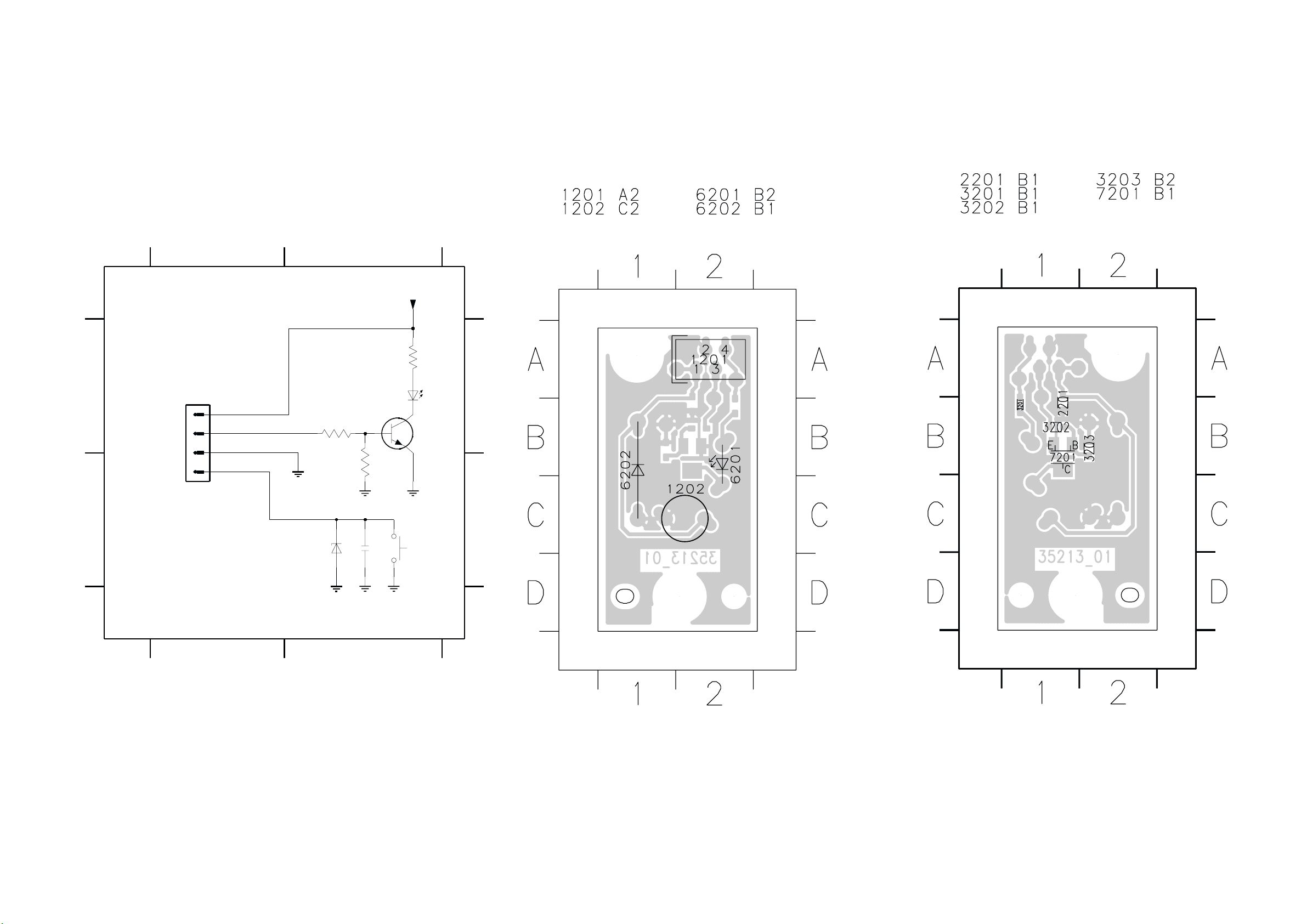
FRONT STANDBY PART - CIRCUIT DIAGRAM
1201 A1
1202 B2
2201 B2
3201 A2
3202 A2
3203 B2
6201 A2
6202 B2
7201 A2
12
A
POWER_ON
STB_SW
FE-BT-VK-N
1201
4
3
2
1
7201
BC847B
3202
4K7
D
D
10K
3203
+5VDSTBY
1K0
6201
D
FRONT STANDBY PART - COMPONENT & CHIP LAYOUT
3201
A
B
B
10n
6202
BZX79-C5V6
D
2201
D
1202
D
STANDBY
12
8239 210 9630 pt3 dd wk0325
8239 210 9630 pt3 dd wk0325
 Loading...