

Philips LPC2114, LPC2124, LPC2212, LPC2214 DATA SHEET

INTEGRATED CIRCUITS
LPC2114/2124/2212/2214
USER MANUAL
Preliminary
Supersedes data of 2004 Feb 03
2004 May 03

Philips Semiconductors Preliminary User Manual
LPC2114/2124/2212/2214ARM-based Microc ontroller
2 May 03, 2004

Philips Semiconductors Preliminary User Manual
LPC2114/2124/2212/2214ARM-based Microc ontroller
Table of Contents
List of Figures . . . . . . . . . . . . . . . . . . . . . . . . . . . . . . . . . . . . . . . . . . . . . . . . . . . . . . . . . . . . . . . . . 7
List of Tables . . . . . . . . . . . . . . . . . . . . . . . . . . . . . . . . . . . . . . . . . . . . . . . . . . . . . . . . . . . . . . . . . . 9
Document Revision History . . . . . . . . . . . . . . . . . . . . . . . . . . . . . . . . . . . . . . . . . . . . . . . . . . . . . . 13
Introduction . . . . . . . . . . . . . . . . . . . . . . . . . . . . . . . . . . . . . . . . . . . . . . . . . . . . . . . . . . . . 15
General Description . . . . . . . . . . . . . . . . . . . . . . . . . . . . . . . . . . . . . . . . . . . . . . . . . . . . . . . . . . . . 15
Features . . . . . . . . . . . . . . . . . . . . . . . . . . . . . . . . . . . . . . . . . . . . . . . . . . . . . . . . . . . . . . . . . . . . . 15
Applications . . . . . . . . . . . . . . . . . . . . . . . . . . . . . . . . . . . . . . . . . . . . . . . . . . . . . . . . . . . . . . . . . . 16
Device information . . . . . . . . . . . . . . . . . . . . . . . . . . . . . . . . . . . . . . . . . . . . . . . . . . . . . . . . . . . . . 16
Architectural Overview . . . . . . . . . . . . . . . . . . . . . . . . . . . . . . . . . . . . . . . . . . . . . . . . . . . . . . . . . . 17
ARM7TDMI-S Processor . . . . . . . . . . . . . . . . . . . . . . . . . . . . . . . . . . . . . . . . . . . . . . . . . . . . . . . . 17
On-Chip Flash Memory System . . . . . . . . . . . . . . . . . . . . . . . . . . . . . . . . . . . . . . . . . . . . . . . . . . . 17
On-Chip Static RAM . . . . . . . . . . . . . . . . . . . . . . . . . . . . . . . . . . . . . . . . . . . . . . . . . . . . . . . . . . . . 18
Block Diagram . . . . . . . . . . . . . . . . . . . . . . . . . . . . . . . . . . . . . . . . . . . . . . . . . . . . . . . . . . . . . . . . 19
LPC2114/2124/2212/2214 Registers . . . . . . . . . . . . . . . . . . . . . . . . . . . . . . . . . . . . . . . . . . . . . . . 20
LPC2114/2124/2212/2214 Memory Addressing . . . . . . . . . . . . . . . . . . . . . . . . . . . . . . . . 33
Memory Maps . . . . . . . . . . . . . . . . . . . . . . . . . . . . . . . . . . . . . . . . . . . . . . . . . . . . . . . . . . . . . . . . 33
LPC2114/2124/2212/2214 Memory Re-mapping and Boot Block . . . . . . . . . . . . . . . . . . . . . . . . . 37
Prefetch Abort and Data Abort Exceptions . . . . . . . . . . . . . . . . . . . . . . . . . . . . . . . . . . . . . . . . . . 40
External Memory Controller (EMC) . . . . . . . . . . . . . . . . . . . . . . . . . . . . . . . . . . . . . . . . . 41
Features . . . . . . . . . . . . . . . . . . . . . . . . . . . . . . . . . . . . . . . . . . . . . . . . . . . . . . . . . . . . . . . . . . . . . 41
Description . . . . . . . . . . . . . . . . . . . . . . . . . . . . . . . . . . . . . . . . . . . . . . . . . . . . . . . . . . . . . . . . . . . 41
Pin Description . . . . . . . . . . . . . . . . . . . . . . . . . . . . . . . . . . . . . . . . . . . . . . . . . . . . . . . . . . . . . . . . 42
Register Description . . . . . . . . . . . . . . . . . . . . . . . . . . . . . . . . . . . . . . . . . . . . . . . . . . . . . . . . . . . . 42
External Memory Interface . . . . . . . . . . . . . . . . . . . . . . . . . . . . . . . . . . . . . . . . . . . . . . . . . . . . . . . 44
Typical Bus Sequences . . . . . . . . . . . . . . . . . . . . . . . . . . . . . . . . . . . . . . . . . . . . . . . . . . . . . . . . . 46
External Memory Selection . . . . . . . . . . . . . . . . . . . . . . . . . . . . . . . . . . . . . . . . . . . . . . . . . . . . . . 47
System Control Block . . . . . . . . . . . . . . . . . . . . . . . . . . . . . . . . . . . . . . . . . . . . . . . . . . . . 49
Summary of System Control Block Functions . . . . . . . . . . . . . . . . . . . . . . . . . . . . . . . . . . . . . . . . 49
Pin Description . . . . . . . . . . . . . . . . . . . . . . . . . . . . . . . . . . . . . . . . . . . . . . . . . . . . . . . . . . . . . . . . 49
Register Description . . . . . . . . . . . . . . . . . . . . . . . . . . . . . . . . . . . . . . . . . . . . . . . . . . . . . . . . . . . . 51
Crystal Oscillator . . . . . . . . . . . . . . . . . . . . . . . . . . . . . . . . . . . . . . . . . . . . . . . . . . . . . . . . . . . . . . 52
External Interrupt Inputs . . . . . . . . . . . . . . . . . . . . . . . . . . . . . . . . . . . . . . . . . . . . . . . . . . . . . . . . . 54
Memory Mapping Control . . . . . . . . . . . . . . . . . . . . . . . . . . . . . . . . . . . . . . . . . . . . . . . . . . . . . . . . 59
PLL (Phase Locked Loop) . . . . . . . . . . . . . . . . . . . . . . . . . . . . . . . . . . . . . . . . . . . . . . . . . . . . . . . 60
Power Control . . . . . . . . . . . . . . . . . . . . . . . . . . . . . . . . . . . . . . . . . . . . . . . . . . . . . . . . . . . . . . . . 66
Power Control Usage Notes . . . . . . . . . . . . . . . . . . . . . . . . . . . . . . . . . . . . . . . . . . . . . . . . . . . . . 68
Reset . . . . . . . . . . . . . . . . . . . . . . . . . . . . . . . . . . . . . . . . . . . . . . . . . . . . . . . . . . . . . . . . . . . . . . . 69
VPB Divider . . . . . . . . . . . . . . . . . . . . . . . . . . . . . . . . . . . . . . . . . . . . . . . . . . . . . . . . . . . . . . . . . . 70
Wakeup Timer . . . . . . . . . . . . . . . . . . . . . . . . . . . . . . . . . . . . . . . . . . . . . . . . . . . . . . . . . . . . . . . . 72
Memory Accelerator Module (MAM) . . . . . . . . . . . . . . . . . . . . . . . . . . . . . . . . . . . . . . . . 73
Introduction . . . . . . . . . . . . . . . . . . . . . . . . . . . . . . . . . . . . . . . . . . . . . . . . . . . . . . . . . . . . . . . . . . 73
Memory Accelerator Module Operating Modes . . . . . . . . . . . . . . . . . . . . . . . . . . . . . . . . . . . . . . . 75
MAM Configuration . . . . . . . . . . . . . . . . . . . . . . . . . . . . . . . . . . . . . . . . . . . . . . . . . . . . . . . . . . . . 76
Register Description . . . . . . . . . . . . . . . . . . . . . . . . . . . . . . . . . . . . . . . . . . . . . . . . . . . . . . . . . . . . 76
MAM Usage Notes . . . . . . . . . . . . . . . . . . . . . . . . . . . . . . . . . . . . . . . . . . . . . . . . . . . . . . . . . . . . . 77
3 May 03, 2004

Philips Semiconductors Preliminary User Manual
LPC2114/2124/2212/2214ARM-based Microc ontroller
Vectored Interrupt Controller (VIC) . . . . . . . . . . . . . . . . . . . . . . . . . . . . . . . . . . . . . . . . . 79
Features . . . . . . . . . . . . . . . . . . . . . . . . . . . . . . . . . . . . . . . . . . . . . . . . . . . . . . . . . . . . . . . . . . . . . 79
Description . . . . . . . . . . . . . . . . . . . . . . . . . . . . . . . . . . . . . . . . . . . . . . . . . . . . . . . . . . . . . . . . . . . 79
Register Description . . . . . . . . . . . . . . . . . . . . . . . . . . . . . . . . . . . . . . . . . . . . . . . . . . . . . . . . . . . . 80
VIC Registers . . . . . . . . . . . . . . . . . . . . . . . . . . . . . . . . . . . . . . . . . . . . . . . . . . . . . . . . . . . . . . . . . 82
Interrupt Sources . . . . . . . . . . . . . . . . . . . . . . . . . . . . . . . . . . . . . . . . . . . . . . . . . . . . . . . . . . . . . . 86
Spurious Interrupts . . . . . . . . . . . . . . . . . . . . . . . . . . . . . . . . . . . . . . . . . . . . . . . . . . . . . . . . . . . . . 88
VIC Usage Notes . . . . . . . . . . . . . . . . . . . . . . . . . . . . . . . . . . . . . . . . . . . . . . . . . . . . . . . . . . . . . . 91
Pin Configuration . . . . . . . . . . . . . . . . . . . . . . . . . . . . . . . . . . . . . . . . . . . . . . . . . . . . . . . 93
LPC2114/2124 Pinout . . . . . . . . . . . . . . . . . . . . . . . . . . . . . . . . . . . . . . . . . . . . . . . . . . . . . . . . . . 93
Pin Description for LPC2114/2124 . . . . . . . . . . . . . . . . . . . . . . . . . . . . . . . . . . . . . . . . . . . . . . . . . 94
LPC2212/2214 Pinout . . . . . . . . . . . . . . . . . . . . . . . . . . . . . . . . . . . . . . . . . . . . . . . . . . . . . . . . . . 98
Pin Description for LPC2212/2214 . . . . . . . . . . . . . . . . . . . . . . . . . . . . . . . . . . . . . . . . . . . . . . . . . 99
Pin Connect Block . . . . . . . . . . . . . . . . . . . . . . . . . . . . . . . . . . . . . . . . . . . . . . . . . . . . . . 109
Features . . . . . . . . . . . . . . . . . . . . . . . . . . . . . . . . . . . . . . . . . . . . . . . . . . . . . . . . . . . . . . . . . . . . 109
Applications . . . . . . . . . . . . . . . . . . . . . . . . . . . . . . . . . . . . . . . . . . . . . . . . . . . . . . . . . . . . . . . . . 109
Description . . . . . . . . . . . . . . . . . . . . . . . . . . . . . . . . . . . . . . . . . . . . . . . . . . . . . . . . . . . . . . . . . . 109
Register Description . . . . . . . . . . . . . . . . . . . . . . . . . . . . . . . . . . . . . . . . . . . . . . . . . . . . . . . . . . . 109
Boot Control on 144-pin Package . . . . . . . . . . . . . . . . . . . . . . . . . . . . . . . . . . . . . . . . . . . . . . . . 114
GPIO . . . . . . . . . . . . . . . . . . . . . . . . . . . . . . . . . . . . . . . . . . . . . . . . . . . . . . . . . . . . . . . . . 115
Features . . . . . . . . . . . . . . . . . . . . . . . . . . . . . . . . . . . . . . . . . . . . . . . . . . . . . . . . . . . . . . . . . . . . 115
Applications . . . . . . . . . . . . . . . . . . . . . . . . . . . . . . . . . . . . . . . . . . . . . . . . . . . . . . . . . . . . . . . . . 115
Pin Description . . . . . . . . . . . . . . . . . . . . . . . . . . . . . . . . . . . . . . . . . . . . . . . . . . . . . . . . . . . . . . . 115
Register Description . . . . . . . . . . . . . . . . . . . . . . . . . . . . . . . . . . . . . . . . . . . . . . . . . . . . . . . . . . . 115
GPIO Usage Notes . . . . . . . . . . . . . . . . . . . . . . . . . . . . . . . . . . . . . . . . . . . . . . . . . . . . . . . . . . . 118
UART0 . . . . . . . . . . . . . . . . . . . . . . . . . . . . . . . . . . . . . . . . . . . . . . . . . . . . . . . . . . . . . . . . 121
Features . . . . . . . . . . . . . . . . . . . . . . . . . . . . . . . . . . . . . . . . . . . . . . . . . . . . . . . . . . . . . . . . . . . . 121
Pin Description . . . . . . . . . . . . . . . . . . . . . . . . . . . . . . . . . . . . . . . . . . . . . . . . . . . . . . . . . . . . . . . 121
Register Description . . . . . . . . . . . . . . . . . . . . . . . . . . . . . . . . . . . . . . . . . . . . . . . . . . . . . . . . . . . 122
Architecture . . . . . . . . . . . . . . . . . . . . . . . . . . . . . . . . . . . . . . . . . . . . . . . . . . . . . . . . . . . . . . . . . 130
UART1 . . . . . . . . . . . . . . . . . . . . . . . . . . . . . . . . . . . . . . . . . . . . . . . . . . . . . . . . . . . . . . . . 133
Features . . . . . . . . . . . . . . . . . . . . . . . . . . . . . . . . . . . . . . . . . . . . . . . . . . . . . . . . . . . . . . . . . . . . 133
Pin Description . . . . . . . . . . . . . . . . . . . . . . . . . . . . . . . . . . . . . . . . . . . . . . . . . . . . . . . . . . . . . . . 133
Register Description . . . . . . . . . . . . . . . . . . . . . . . . . . . . . . . . . . . . . . . . . . . . . . . . . . . . . . . . . . . 134
Architecture . . . . . . . . . . . . . . . . . . . . . . . . . . . . . . . . . . . . . . . . . . . . . . . . . . . . . . . . . . . . . . . . . 145
I2C Interface . . . . . . . . . . . . . . . . . . . . . . . . . . . . . . . . . . . . . . . . . . . . . . . . . . . . . . . . . . . 147
Features . . . . . . . . . . . . . . . . . . . . . . . . . . . . . . . . . . . . . . . . . . . . . . . . . . . . . . . . . . . . . . . . . . . . 147
Applications . . . . . . . . . . . . . . . . . . . . . . . . . . . . . . . . . . . . . . . . . . . . . . . . . . . . . . . . . . . . . . . . . 147
Description . . . . . . . . . . . . . . . . . . . . . . . . . . . . . . . . . . . . . . . . . . . . . . . . . . . . . . . . . . . . . . . . . . 147
Pin Description . . . . . . . . . . . . . . . . . . . . . . . . . . . . . . . . . . . . . . . . . . . . . . . . . . . . . . . . . . . . . . . 151
Register Description . . . . . . . . . . . . . . . . . . . . . . . . . . . . . . . . . . . . . . . . . . . . . . . . . . . . . . . . . . . 152
Architecture . . . . . . . . . . . . . . . . . . . . . . . . . . . . . . . . . . . . . . . . . . . . . . . . . . . . . . . . . . . . . . . . . 158
SPI Interface . . . . . . . . . . . . . . . . . . . . . . . . . . . . . . . . . . . . . . . . . . . . . . . . . . . . . . . . . . . 159
Features . . . . . . . . . . . . . . . . . . . . . . . . . . . . . . . . . . . . . . . . . . . . . . . . . . . . . . . . . . . . . . . . . . . . 159
Description . . . . . . . . . . . . . . . . . . . . . . . . . . . . . . . . . . . . . . . . . . . . . . . . . . . . . . . . . . . . . . . . . . 159
Pin Description . . . . . . . . . . . . . . . . . . . . . . . . . . . . . . . . . . . . . . . . . . . . . . . . . . . . . . . . . . . . . . . 163
Register Description . . . . . . . . . . . . . . . . . . . . . . . . . . . . . . . . . . . . . . . . . . . . . . . . . . . . . . . . . . . 164
Architecture . . . . . . . . . . . . . . . . . . . . . . . . . . . . . . . . . . . . . . . . . . . . . . . . . . . . . . . . . . . . . . . . . 167
4 May 03, 2004

Philips Semiconductors Preliminary User Manual
LPC2114/2124/2212/2214ARM-based Microc ontroller
Timer0 and Timer1 . . . . . . . . . . . . . . . . . . . . . . . . . . . . . . . . . . . . . . . . . . . . . . . . . . . . . . 169
Features . . . . . . . . . . . . . . . . . . . . . . . . . . . . . . . . . . . . . . . . . . . . . . . . . . . . . . . . . . . . . . . . . . . . 169
Applications . . . . . . . . . . . . . . . . . . . . . . . . . . . . . . . . . . . . . . . . . . . . . . . . . . . . . . . . . . . . . . . . . 169
Description . . . . . . . . . . . . . . . . . . . . . . . . . . . . . . . . . . . . . . . . . . . . . . . . . . . . . . . . . . . . . . . . . . 170
Pin Description . . . . . . . . . . . . . . . . . . . . . . . . . . . . . . . . . . . . . . . . . . . . . . . . . . . . . . . . . . . . . . . 170
Register Description . . . . . . . . . . . . . . . . . . . . . . . . . . . . . . . . . . . . . . . . . . . . . . . . . . . . . . . . . . . 171
Example Timer Operation . . . . . . . . . . . . . . . . . . . . . . . . . . . . . . . . . . . . . . . . . . . . . . . . . . . . . . 176
Architecture . . . . . . . . . . . . . . . . . . . . . . . . . . . . . . . . . . . . . . . . . . . . . . . . . . . . . . . . . . . . . . . . . 177
Pulse Width Modulator (PWM) . . . . . . . . . . . . . . . . . . . . . . . . . . . . . . . . . . . . . . . . . . . . 179
Features . . . . . . . . . . . . . . . . . . . . . . . . . . . . . . . . . . . . . . . . . . . . . . . . . . . . . . . . . . . . . . . . . . . . 179
Description . . . . . . . . . . . . . . . . . . . . . . . . . . . . . . . . . . . . . . . . . . . . . . . . . . . . . . . . . . . . . . . . . . 179
Pin Description . . . . . . . . . . . . . . . . . . . . . . . . . . . . . . . . . . . . . . . . . . . . . . . . . . . . . . . . . . . . . . . 184
Register Description . . . . . . . . . . . . . . . . . . . . . . . . . . . . . . . . . . . . . . . . . . . . . . . . . . . . . . . . . . . 185
A/D Converter . . . . . . . . . . . . . . . . . . . . . . . . . . . . . . . . . . . . . . . . . . . . . . . . . . . . . . . . . 193
Features . . . . . . . . . . . . . . . . . . . . . . . . . . . . . . . . . . . . . . . . . . . . . . . . . . . . . . . . . . . . . . . . . . . . 193
Description . . . . . . . . . . . . . . . . . . . . . . . . . . . . . . . . . . . . . . . . . . . . . . . . . . . . . . . . . . . . . . . . . . 193
Pin DescriptionS . . . . . . . . . . . . . . . . . . . . . . . . . . . . . . . . . . . . . . . . . . . . . . . . . . . . . . . . . . . . . 193
Register Description . . . . . . . . . . . . . . . . . . . . . . . . . . . . . . . . . . . . . . . . . . . . . . . . . . . . . . . . . . . 193
OPERATION . . . . . . . . . . . . . . . . . . . . . . . . . . . . . . . . . . . . . . . . . . . . . . . . . . . . . . . . . . . . . . . . 195
Real Time Clock . . . . . . . . . . . . . . . . . . . . . . . . . . . . . . . . . . . . . . . . . . . . . . . . . . . . . . . . 197
Features . . . . . . . . . . . . . . . . . . . . . . . . . . . . . . . . . . . . . . . . . . . . . . . . . . . . . . . . . . . . . . . . . . . . 197
Description . . . . . . . . . . . . . . . . . . . . . . . . . . . . . . . . . . . . . . . . . . . . . . . . . . . . . . . . . . . . . . . . . . 197
Architecture . . . . . . . . . . . . . . . . . . . . . . . . . . . . . . . . . . . . . . . . . . . . . . . . . . . . . . . . . . . . . . . . . 198
Register Description . . . . . . . . . . . . . . . . . . . . . . . . . . . . . . . . . . . . . . . . . . . . . . . . . . . . . . . . . . . 198
RTC Interrupts . . . . . . . . . . . . . . . . . . . . . . . . . . . . . . . . . . . . . . . . . . . . . . . . . . . . . . . . . . . . . . . 200
Miscellaneous Register Group . . . . . . . . . . . . . . . . . . . . . . . . . . . . . . . . . . . . . . . . . . . . . . . . . . . 201
Consolidated Time Registers . . . . . . . . . . . . . . . . . . . . . . . . . . . . . . . . . . . . . . . . . . . . . . . . . . . . 204
Time Counter Group . . . . . . . . . . . . . . . . . . . . . . . . . . . . . . . . . . . . . . . . . . . . . . . . . . . . . . . . . . 206
Alarm Register Group . . . . . . . . . . . . . . . . . . . . . . . . . . . . . . . . . . . . . . . . . . . . . . . . . . . . . . . . . 207
RTC Usage Notes . . . . . . . . . . . . . . . . . . . . . . . . . . . . . . . . . . . . . . . . . . . . . . . . . . . . . . . . . . . . 207
Reference Clock Divider (Prescaler) . . . . . . . . . . . . . . . . . . . . . . . . . . . . . . . . . . . . . . . . . . . . . . 208
Watchdog . . . . . . . . . . . . . . . . . . . . . . . . . . . . . . . . . . . . . . . . . . . . . . . . . . . . . . . . . . . . . 211
Features . . . . . . . . . . . . . . . . . . . . . . . . . . . . . . . . . . . . . . . . . . . . . . . . . . . . . . . . . . . . . . . . . . . . 211
Applications . . . . . . . . . . . . . . . . . . . . . . . . . . . . . . . . . . . . . . . . . . . . . . . . . . . . . . . . . . . . . . . . . 211
Description . . . . . . . . . . . . . . . . . . . . . . . . . . . . . . . . . . . . . . . . . . . . . . . . . . . . . . . . . . . . . . . . . . 211
Register Description . . . . . . . . . . . . . . . . . . . . . . . . . . . . . . . . . . . . . . . . . . . . . . . . . . . . . . . . . . . 212
Usage Notes on Watchdog Reset and External Start . . . . . . . . . . . . . . . . . . . . . . . . . . . . . . . . . 214
. . . . . . . . . . . . . . . . . . . . . . . . . . . . . . . . . . . . . . . . . . . . . . . . . . . . . . . . . . . . . . . . . . . . . . . . . . . 215
Block Diagram . . . . . . . . . . . . . . . . . . . . . . . . . . . . . . . . . . . . . . . . . . . . . . . . . . . . . . . . . . . . . . . 216
Flash Memory System and Programming . . . . . . . . . . . . . . . . . . . . . . . . . . . . . . . . . . . 217
Flash Memory System . . . . . . . . . . . . . . . . . . . . . . . . . . . . . . . . . . . . . . . . . . . . . . . . . . . . . . . . . 217
Flash boot Loader . . . . . . . . . . . . . . . . . . . . . . . . . . . . . . . . . . . . . . . . . . . . . . . . . . . . . . . . . . . . 217
Features . . . . . . . . . . . . . . . . . . . . . . . . . . . . . . . . . . . . . . . . . . . . . . . . . . . . . . . . . . . . . . . . . . . . 217
Applications . . . . . . . . . . . . . . . . . . . . . . . . . . . . . . . . . . . . . . . . . . . . . . . . . . . . . . . . . . . . . . . . . 217
Description . . . . . . . . . . . . . . . . . . . . . . . . . . . . . . . . . . . . . . . . . . . . . . . . . . . . . . . . . . . . . . . . . . 217
Boot process FlowChart . . . . . . . . . . . . . . . . . . . . . . . . . . . . . . . . . . . . . . . . . . . . . . . . . . . . . . . . 221
Sector Numbers . . . . . . . . . . . . . . . . . . . . . . . . . . . . . . . . . . . . . . . . . . . . . . . . . . . . . . . . . . . . . . 223
Code Read Protection . . . . . . . . . . . . . . . . . . . . . . . . . . . . . . . . . . . . . . . . . . . . . . . . . . . . . . . . . 224
JTAG FLASH Programming interface . . . . . . . . . . . . . . . . . . . . . . . . . . . . . . . . . . . . . . . . . . . . . 240
5 May 03, 2004

Philips Semiconductors Preliminary User Manual
LPC2114/2124/2212/2214ARM-based Microc ontroller
EmbeddedICE Logic . . . . . . . . . . . . . . . . . . . . . . . . . . . . . . . . . . . . . . . . . . . . . . . . . . . . 241
Features . . . . . . . . . . . . . . . . . . . . . . . . . . . . . . . . . . . . . . . . . . . . . . . . . . . . . . . . . . . . . . . . . . . . 241
Applications . . . . . . . . . . . . . . . . . . . . . . . . . . . . . . . . . . . . . . . . . . . . . . . . . . . . . . . . . . . . . . . . . 241
Description . . . . . . . . . . . . . . . . . . . . . . . . . . . . . . . . . . . . . . . . . . . . . . . . . . . . . . . . . . . . . . . . . . 241
Pin Description . . . . . . . . . . . . . . . . . . . . . . . . . . . . . . . . . . . . . . . . . . . . . . . . . . . . . . . . . . . . . . . 242
Reset State of Multiplexed Pins . . . . . . . . . . . . . . . . . . . . . . . . . . . . . . . . . . . . . . . . . . . . . . . . . . 242
Register Description . . . . . . . . . . . . . . . . . . . . . . . . . . . . . . . . . . . . . . . . . . . . . . . . . . . . . . . . . . . 243
Block Diagram . . . . . . . . . . . . . . . . . . . . . . . . . . . . . . . . . . . . . . . . . . . . . . . . . . . . . . . . . . . . . . . 244
Embedded Trace Macrocell . . . . . . . . . . . . . . . . . . . . . . . . . . . . . . . . . . . . . . . . . . . . . . 245
Features . . . . . . . . . . . . . . . . . . . . . . . . . . . . . . . . . . . . . . . . . . . . . . . . . . . . . . . . . . . . . . . . . . . . 245
Applications . . . . . . . . . . . . . . . . . . . . . . . . . . . . . . . . . . . . . . . . . . . . . . . . . . . . . . . . . . . . . . . . . 245
Description . . . . . . . . . . . . . . . . . . . . . . . . . . . . . . . . . . . . . . . . . . . . . . . . . . . . . . . . . . . . . . . . . . 245
Pin Description . . . . . . . . . . . . . . . . . . . . . . . . . . . . . . . . . . . . . . . . . . . . . . . . . . . . . . . . . . . . . . . 246
Reset State of Multiplexed Pins . . . . . . . . . . . . . . . . . . . . . . . . . . . . . . . . . . . . . . . . . . . . . . . . . . 246
Register Description . . . . . . . . . . . . . . . . . . . . . . . . . . . . . . . . . . . . . . . . . . . . . . . . . . . . . . . . . . . 247
Block Diagram . . . . . . . . . . . . . . . . . . . . . . . . . . . . . . . . . . . . . . . . . . . . . . . . . . . . . . . . . . . . . . . 248
RealMonitor . . . . . . . . . . . . . . . . . . . . . . . . . . . . . . . . . . . . . . . . . . . . . . . . . . . . . . . . . . . 249
Features . . . . . . . . . . . . . . . . . . . . . . . . . . . . . . . . . . . . . . . . . . . . . . . . . . . . . . . . . . . . . . . . . . . . 249
Applications . . . . . . . . . . . . . . . . . . . . . . . . . . . . . . . . . . . . . . . . . . . . . . . . . . . . . . . . . . . . . . . . . 249
Description . . . . . . . . . . . . . . . . . . . . . . . . . . . . . . . . . . . . . . . . . . . . . . . . . . . . . . . . . . . . . . . . . . 249
How to Enable RealMonitor . . . . . . . . . . . . . . . . . . . . . . . . . . . . . . . . . . . . . . . . . . . . . . . . . . . . . 253
RealMonitor build options . . . . . . . . . . . . . . . . . . . . . . . . . . . . . . . . . . . . . . . . . . . . . . . . . . . . . . 259
6 May 03, 2004

Philips Semiconductors Preliminary User Manual
LPC2114/2124/2212/2214ARM-based Microc ontroller
List of Figures
Figure 1: LPC2114/2124/2212/2214 Block Diagram . . . . . . . . . . . . . . . . . . . . . . . . . . . . . . . . . . . . . . . . . 19
Figure 2: System Memory Map . . . . . . . . . . . . . . . . . . . . . . . . . . . . . . . . . . . . . . . . . . . . . . . . . . . . . . . . . 33
Figure 3: Peripheral Memory Map. . . . . . . . . . . . . . . . . . . . . . . . . . . . . . . . . . . . . . . . . . . . . . . . . . . . . . . 34
Figure 4: AHB Peripheral Map. . . . . . . . . . . . . . . . . . . . . . . . . . . . . . . . . . . . . . . . . . . . . . . . . . . . . . . . . . 35
Figure 5: VPB Peripheral Map. . . . . . . . . . . . . . . . . . . . . . . . . . . . . . . . . . . . . . . . . . . . . . . . . . . . . . . . . . 36
Figure 6: Map of lower memory is showing re-mapped and re-mappable areas (128 kB Flash).. . . . . . . 39
Figure 7: 32 Bit Bank External Memory Interfaces . . . . . . . . . . . . . . . . . . . . . . . . . . . . . . . . . . . . . . . . . . 44
Figure 8: 16 Bit Bank External Memory Interfaces . . . . . . . . . . . . . . . . . . . . . . . . . . . . . . . . . . . . . . . . . . 45
Figure 9: 8 Bit Bank External Memory Interface . . . . . . . . . . . . . . . . . . . . . . . . . . . . . . . . . . . . . . . . . . . . 45
Figure 10: External memory read access (WST1=0 and WST1=1 examples) . . . . . . . . . . . . . . . . . . . . . . 46
Figure 11: External memory write access (WST2=0 and WST2=1 examples) . . . . . . . . . . . . . . . . . . . . . . 46
Figure 12: Oscillator modes and models: a) slave mode of operation, b) oscillation mode of operation,
c) external crystal model used for CX1/X2 evaluation . . . . . . . . . . . . . . . . . . . . . . . . . . . . . . . . 52
Figure 13: FOSC selection algorithm. . . . . . . . . . . . . . . . . . . . . . . . . . . . . . . . . . . . . . . . . . . . . . . . . . . . . . 53
Figure 14: External Interrupt Logic. . . . . . . . . . . . . . . . . . . . . . . . . . . . . . . . . . . . . . . . . . . . . . . . . . . . . . . . 58
Figure 15: PLL Block Diagram. . . . . . . . . . . . . . . . . . . . . . . . . . . . . . . . . . . . . . . . . . . . . . . . . . . . . . . . . . . 61
Figure 16: Reset Block Diagram including Wakeup Timer . . . . . . . . . . . . . . . . . . . . . . . . . . . . . . . . . . . . . 69
Figure 17: VPB Divider Connections. . . . . . . . . . . . . . . . . . . . . . . . . . . . . . . . . . . . . . . . . . . . . . . . . . . . . . 71
Figure 18: Simplified Block Diagram of the Memory Accelerator Module . . . . . . . . . . . . . . . . . . . . . . . . . . 74
Figure 19: Block Diagram of the Vectored Interrupt Controller . . . . . . . . . . . . . . . . . . . . . . . . . . . . . . . . . . 87
Figure 20: LPC2114/2124 64-pin package . . . . . . . . . . . . . . . . . . . . . . . . . . . . . . . . . . . . . . . . . . . . . . . . . 93
Figure 21: LPC2212/2214 144-pin package . . . . . . . . . . . . . . . . . . . . . . . . . . . . . . . . . . . . . . . . . . . . . . . . 98
Figure 22: UART0 Block Diagram . . . . . . . . . . . . . . . . . . . . . . . . . . . . . . . . . . . . . . . . . . . . . . . . . . . . . . . 131
Figure 23: UART1 Block Diagram . . . . . . . . . . . . . . . . . . . . . . . . . . . . . . . . . . . . . . . . . . . . . . . . . . . . . . . 146
Figure 24: I2C Bus Configuration. . . . . . . . . . . . . . . . . . . . . . . . . . . . . . . . . . . . . . . . . . . . . . . . . . . . . . . . 148
Figure 25: Slave Mode Configuration . . . . . . . . . . . . . . . . . . . . . . . . . . . . . . . . . . . . . . . . . . . . . . . . . . . . 148
Figure 26: Format in the master transmitter mode. . . . . . . . . . . . . . . . . . . . . . . . . . . . . . . . . . . . . . . . . . . 149
Figure 27: Format of master receiver mode. . . . . . . . . . . . . . . . . . . . . . . . . . . . . . . . . . . . . . . . . . . . . . . . 149
Figure 28: A master receiver switch to master transmitter after sending repeated START. . . . . . . . . . . . 150
Figure 29: Slave Mode Configuration . . . . . . . . . . . . . . . . . . . . . . . . . . . . . . . . . . . . . . . . . . . . . . . . . . . . 150
Figure 30: Format of slave receiver mode. . . . . . . . . . . . . . . . . . . . . . . . . . . . . . . . . . . . . . . . . . . . . . . . . 151
Figure 31: Format of slave transmitter mode. . . . . . . . . . . . . . . . . . . . . . . . . . . . . . . . . . . . . . . . . . . . . . . 151
Figure 32: I2C Architecture . . . . . . . . . . . . . . . . . . . . . . . . . . . . . . . . . . . . . . . . . . . . . . . . . . . . . . . . . . . . 158
Figure 33: SPI Data Transfer Format (CPHA = 0 and CPHA = 1). . . . . . . . . . . . . . . . . . . . . . . . . . . . . . . 160
Figure 34: SPI Block Diagram . . . . . . . . . . . . . . . . . . . . . . . . . . . . . . . . . . . . . . . . . . . . . . . . . . . . . . . . . . 167
Figure 35: A timer cycle in which PR=2, MRx=6, and both interrupt and reset on match are enabled.. . . 176
Figure 36: A timer cycle in which PR=2, MRx=6, and both interrupt and stop on match are enabled. . . . 176
Figure 37: Timer block diagram. . . . . . . . . . . . . . . . . . . . . . . . . . . . . . . . . . . . . . . . . . . . . . . . . . . . . . . . . 177
Figure 38: PWM block diagram . . . . . . . . . . . . . . . . . . . . . . . . . . . . . . . . . . . . . . . . . . . . . . . . . . . . . . . . . 181
Figure 39: Sample PWM waveforms. . . . . . . . . . . . . . . . . . . . . . . . . . . . . . . . . . . . . . . . . . . . . . . . . . . . . 182
Figure 40: RTC block diagram. . . . . . . . . . . . . . . . . . . . . . . . . . . . . . . . . . . . . . . . . . . . . . . . . . . . . . . . . . 198
Figure 41: RTC Prescaler block diagram. . . . . . . . . . . . . . . . . . . . . . . . . . . . . . . . . . . . . . . . . . . . . . . . . . 209
Figure 42: Watchdog Block Diagram. . . . . . . . . . . . . . . . . . . . . . . . . . . . . . . . . . . . . . . . . . . . . . . . . . . . . 216
Figure 43: Map of lower memory after any reset (128 kB Flash part).. . . . . . . . . . . . . . . . . . . . . . . . . . . . 218
Figure 44: Boot Process flowchart (Bootloader revisions before 1.61) . . . . . . . . . . . . . . . . . . . . . . . . . . . 221
Figure 45: Boot Process flowchart (Bootloader revisions 1.61 and later) . . . . . . . . . . . . . . . . . . . . . . . . . 222
Figure 46: IAP Parameter passing. . . . . . . . . . . . . . . . . . . . . . . . . . . . . . . . . . . . . . . . . . . . . . . . . . . . . . . 236
Figure 47: EmbeddedICE Debug Environment Block Diagram. . . . . . . . . . . . . . . . . . . . . . . . . . . . . . . . . 244
Figure 48: ETM Debug Environment Block Diagram. . . . . . . . . . . . . . . . . . . . . . . . . . . . . . . . . . . . . . . . . 248
Figure 49: RealMonitor components . . . . . . . . . . . . . . . . . . . . . . . . . . . . . . . . . . . . . . . . . . . . . . . . . . . . . 250
Figure 50: RealMonitor as a state machine. . . . . . . . . . . . . . . . . . . . . . . . . . . . . . . . . . . . . . . . . . . . . . . . 251
Figure 51: Exception Handlers. . . . . . . . . . . . . . . . . . . . . . . . . . . . . . . . . . . . . . . . . . . . . . . . . . . . . . . . . . 254
7 May 03, 2004

Philips Semiconductors Preliminary User Manual
LPC2114/2124/2212/2214ARM-based Microc ontroller
8 May 03, 2004

Philips Semiconductors Preliminary User Manual
LPC2114/2124/2212/2214ARM-based Microc ontroller
List of Tables
Table 1: LPC2114/2124/2212/2214 device information. . . . . . . . . . . . . . . . . . . . . . . . . . . . . . . . . . . . . . . 16
Table 2: LPC2114/2124/2212/2214 Registers. . . . . . . . . . . . . . . . . . . . . . . . . . . . . . . . . . . . . . . . . . . . . . 20
Table 3: ARM Exception Vector Locations. . . . . . . . . . . . . . . . . . . . . . . . . . . . . . . . . . . . . . . . . . . . . . . . . 37
Table 4: LPC2114/2124/2212/2214 Memory Mapping Modes. . . . . . . . . . . . . . . . . . . . . . . . . . . . . . . . . . 37
Table 5: Address Ranges of External Memory Banks (LPC2212/2214 only) . . . . . . . . . . . . . . . . . . . . . . 41
Table 6: External Memory Controller Pin Description . . . . . . . . . . . . . . . . . . . . . . . . . . . . . . . . . . . . . . . . 42
Table 7: External Memory Controller Register Map. . . . . . . . . . . . . . . . . . . . . . . . . . . . . . . . . . . . . . . . . . 42
Table 8: Bank Configuration Registers 0-3 (BCFG0-3 - 0xFFE00000-0C). . . . . . . . . . . . . . . . . . . . . . . . 43
Table 9: Default memory widths at Reset . . . . . . . . . . . . . . . . . . . . . . . . . . . . . . . . . . . . . . . . . . . . . . . . . 43
Table 10: External memory and system requirements. . . . . . . . . . . . . . . . . . . . . . . . . . . . . . . . . . . . . . . . . 47
Table 11: Pin summary . . . . . . . . . . . . . . . . . . . . . . . . . . . . . . . . . . . . . . . . . . . . . . . . . . . . . . . . . . . . . . . . 49
Table 12: Summary of System Control Registers . . . . . . . . . . . . . . . . . . . . . . . . . . . . . . . . . . . . . . . . . . . . 51
Table 13: Recommended values for CX1/X2 in oscillation mode
(crystal and external components parameters) . . . . . . . . . . . . . . . . . . . . . . . . . . . . . . . . . . . . . . 52
Table 14: External Interrupt Registers. . . . . . . . . . . . . . . . . . . . . . . . . . . . . . . . . . . . . . . . . . . . . . . . . . . . . 54
Table 15: External Interrupt Flag Register (EXTINT - 0xE01FC140). . . . . . . . . . . . . . . . . . . . . . . . . . . . . . 55
Table 16: External Interrupt Wakeup Register (EXTWAKE - 0xE01FC144) . . . . . . . . . . . . . . . . . . . . . . . . 56
Table 17: External Interrupt Mode Register (EXTMODE - 0xE01FC148) . . . . . . . . . . . . . . . . . . . . . . . . . . 56
Table 18: External Interrupt Polarity Register (EXTPOLAR - 0xE01FC14C). . . . . . . . . . . . . . . . . . . . . . . . 57
Table 19: MEMMAP Register. . . . . . . . . . . . . . . . . . . . . . . . . . . . . . . . . . . . . . . . . . . . . . . . . . . . . . . . . . . . 59
Table 20: Memory Mapping Control Register (MEMMAP - 0xE01FC040). . . . . . . . . . . . . . . . . . . . . . . . . . 59
Table 21: PLL Registers. . . . . . . . . . . . . . . . . . . . . . . . . . . . . . . . . . . . . . . . . . . . . . . . . . . . . . . . . . . . . . . . 60
Table 22: PLL Control Register (PLLCON - 0xE01FC080) . . . . . . . . . . . . . . . . . . . . . . . . . . . . . . . . . . . . . 62
Table 23: PLL Configuration Register (PLLCFG - 0xE01FC084) . . . . . . . . . . . . . . . . . . . . . . . . . . . . . . . . 62
Table 24: PLL Status Register (PLLSTAT - 0xE01FC088) . . . . . . . . . . . . . . . . . . . . . . . . . . . . . . . . . . . . . 63
Table 25: PLL Control Bit Combinations . . . . . . . . . . . . . . . . . . . . . . . . . . . . . . . . . . . . . . . . . . . . . . . . . . . 63
Table 26: PLL Feed Register (PLLFEED - 0xE01FC08C). . . . . . . . . . . . . . . . . . . . . . . . . . . . . . . . . . . . . . 64
Table 27: PLL Divider Values. . . . . . . . . . . . . . . . . . . . . . . . . . . . . . . . . . . . . . . . . . . . . . . . . . . . . . . . . . . . 65
Table 28: PLL Multiplier Values. . . . . . . . . . . . . . . . . . . . . . . . . . . . . . . . . . . . . . . . . . . . . . . . . . . . . . . . . . 65
Table 29: Power Control Registers . . . . . . . . . . . . . . . . . . . . . . . . . . . . . . . . . . . . . . . . . . . . . . . . . . . . . . . 66
Table 30: Power Control Register (PCON - 0xE01FC0C0). . . . . . . . . . . . . . . . . . . . . . . . . . . . . . . . . . . . . 66
Table 31: Power Control for Peripherals Register for LPC2114/2124 (PCONP - 0xE01FC0C4) . . . . . . . . 67
Table 32: Power Control for Peripherals Register for LPC2212/2214 (PCONP - 0xE01FC0C4) . . . . . . . . 67
Table 33: VPBDIV Register Map . . . . . . . . . . . . . . . . . . . . . . . . . . . . . . . . . . . . . . . . . . . . . . . . . . . . . . . . . 70
Table 34: VPB Divider Register (VPBDIV - 0xE01FC100). . . . . . . . . . . . . . . . . . . . . . . . . . . . . . . . . . . . . . 70
Table 35: MAM Responses to Program Accesses of Various Types. . . . . . . . . . . . . . . . . . . . . . . . . . . . . . 75
Table 36: MAM Responses to Data and DMA Accesses of Various Types. . . . . . . . . . . . . . . . . . . . . . . . . 75
Table 37: Summary of System Control Registers . . . . . . . . . . . . . . . . . . . . . . . . . . . . . . . . . . . . . . . . . . . . 76
Table 38: MAM Control Register (MAMCR - 0xE01FC000). . . . . . . . . . . . . . . . . . . . . . . . . . . . . . . . . . . . . 77
Table 39: MAM Timing Register (MAMTIM - 0xE01FC004) . . . . . . . . . . . . . . . . . . . . . . . . . . . . . . . . . . . . 77
Table 40: VIC Register Map. . . . . . . . . . . . . . . . . . . . . . . . . . . . . . . . . . . . . . . . . . . . . . . . . . . . . . . . . . . . . 80
Table 41: Software Interrupt Register (VICSoftInt - 0xFFFFF018, Read/Write) . . . . . . . . . . . . . . . . . . . . . 82
Table 42: Software Interrupt Clear Register (VICSoftIntClear - 0xFFFFF01C, Write Only). . . . . . . . . . . . . 82
Table 43: Raw Interrupt Status Register (VICRawIntr - 0xFFFFF008, Read-Only). . . . . . . . . . . . . . . . . . . 82
Table 44: Interrupt Enable Register (VICINtEnable - 0xFFFFF010, Read/Write) . . . . . . . . . . . . . . . . . . . . 83
Table 45: Software Interrupt Clear Register (VICIntEnClear - 0xFFFFF014, Write Only) . . . . . . . . . . . . . . 83
Table 46: Interrupt Select Register (VICIntSelect - 0xFFFFF00C, Read/Write) . . . . . . . . . . . . . . . . . . . . . 83
Table 47: IRQ Status Register (VICIRQStatus - 0xFFFFF000, Read-Only) . . . . . . . . . . . . . . . . . . . . . . . . 83
Table 48: IRQ Status Register (VICFIQStatus - 0xFFFFF004, Read-Only) . . . . . . . . . . . . . . . . . . . . . . . . 84
Table 49: Vector Control Registers (VICVectCntl0-15 - 0xFFFFF200-23C, Read/Write) . . . . . . . . . . . . . . 84
Table 50: Vector Address Registers (VICVectAddr0-15 - 0xFFFFF100-13C, Read/Write). . . . . . . . . . . . . 84
Table 51: Default Vector Address Register (VICDefVectAddr - 0xFFFFF034, Read/Write) . . . . . . . . . . . . 84
Table 52: Vector Address Register (VICVectAddr - 0xFFFFF030, Read/Write). . . . . . . . . . . . . . . . . . . . . 85
Table 53: Protection Enable Register (VICProtection - 0xFFFFF020, Read/Write). . . . . . . . . . . . . . . . . . . 85
Table 54: Connection of Interrupt Sources to the Vectored Interrupt Controller . . . . . . . . . . . . . . . . . . . . . 86
9 May 03, 2004

Philips Semiconductors Preliminary User Manual
LPC2114/2124/2212/2214ARM-based Microc ontroller
Table 55: Pin description for LPC2114/2124 . . . . . . . . . . . . . . . . . . . . . . . . . . . . . . . . . . . . . . . . . . . . . . . . 94
Table 56: Pin description for LPC2212/2214 . . . . . . . . . . . . . . . . . . . . . . . . . . . . . . . . . . . . . . . . . . . . . . . . 99
Table 57: Pin Connect Block Register Map. . . . . . . . . . . . . . . . . . . . . . . . . . . . . . . . . . . . . . . . . . . . . . . . 109
Table 58: Pin Function Select Register 0 for LPC2114/2124/2212/2214 (PINSEL0 - 0xE002C000). . . . 110
Table 59: Pin Function Select Register 1 for LPC2114/2124/2212/2214 (PINSEL1 - 0xE002C004) . . . . 110
Table 60: Pin Function Select Register 2 for LPC2114/2124 (PINSEL2 - 0xE002C014) . . . . . . . . . . . . . 111
Table 61: Pin Function Select Register 2 for LPC2212/2214 (PINSEL2 - 0xE002C014) . . . . . . . . . . . . . 112
Table 62: Pin Function Select Register Bits. . . . . . . . . . . . . . . . . . . . . . . . . . . . . . . . . . . . . . . . . . . . . . . . 113
Table 63: Boot Control on BOOT1:0 . . . . . . . . . . . . . . . . . . . . . . . . . . . . . . . . . . . . . . . . . . . . . . . . . . . . . 114
Table 64: GPIO Pin Description. . . . . . . . . . . . . . . . . . . . . . . . . . . . . . . . . . . . . . . . . . . . . . . . . . . . . . . . . 115
Table 65: GPIO Register Map . . . . . . . . . . . . . . . . . . . . . . . . . . . . . . . . . . . . . . . . . . . . . . . . . . . . . . . . . . 116
Table 66: GPIO Pin Value Register (IO0PIN - 0xE0028000, IO1PIN - 0xE0028010,
IO2PIN - 0xE0028020, IO3PIN - 0xE0028030) . . . . . . . . . . . . . . . . . . . . . . . . . . . . . . . . . . . . . 117
Table 67: GPIO Output Set Register (IO0SET - 0xE0028004, IO1SET - 0xE0028014,
IO2SET - 0xE0028024, IO3SET - 0xE0028034) . . . . . . . . . . . . . . . . . . . . . . . . . . . . . . . . . . . . 117
Table 68: GPIO Output Clear Register (IO0CLR - 0xE002800C, IO1CLR - 0xE002801C,
IO2CLR - 0xE002802C, IO3CLR - 0xE002803C) . . . . . . . . . . . . . . . . . . . . . . . . . . . . . . . . . . . 118
Table 69: GPIO Direction Register (IO0DIR - 0xE0028008, IO1DIR - 0xE0028018,
IO2DIR - 0xE0028028, IO3DIR - 0xE0028038). . . . . . . . . . . . . . . . . . . . . . . . . . . . . . . . . . . . . 118
Table 70: UART0 Pin Description . . . . . . . . . . . . . . . . . . . . . . . . . . . . . . . . . . . . . . . . . . . . . . . . . . . . . . . 121
Table 71: UART0 Register Map. . . . . . . . . . . . . . . . . . . . . . . . . . . . . . . . . . . . . . . . . . . . . . . . . . . . . . . . . 122
Table 72: UART0 Receiver Buffer Register (U0RBR - 0xE000C000 when DLAB = 0, Read Only). . . . . . 123
Table 73: UART0 Transmit Holding Register (U0THR - 0xE000C000 when DLAB = 0, Write Only). . . . . 123
Table 74: UART0 Divisor Latch LSB Register (U0DLL - 0xE000C000 when DLAB = 1). . . . . . . . . . . . . . 123
Table 75: UART0 Divisor Latch MSB Register (U0DLM - 0xE000C004 when DLAB = 1). . . . . . . . . . . . . 123
Table 76: UART0 Interrupt Enable Register Bit Descriptions (U0IER - 0xE000C004 when DLAB = 0) . . 124
Table 77: UART0 Interrupt Identification Register Bit Descriptions (U0IIR - 0xE000C008, Read Only) . . 124
Table 78: UART0 Interrupt Handling . . . . . . . . . . . . . . . . . . . . . . . . . . . . . . . . . . . . . . . . . . . . . . . . . . . . . 125
Table 79: UART0 FIFO Control Register Bit Descriptions (U0FCR - 0xE000C008) . . . . . . . . . . . . . . . . . 126
Table 80: UART0 Line Control Register Bit Descriptions (U0LCR - 0xE000C00C). . . . . . . . . . . . . . . . . . 127
Table 81: UART0 Line Status Register Bit Descriptions (U0LSR - 0xE000C014, Read Only) . . . . . . . . . 128
Table 82: UART0 Scratchpad Register (U0SCR - 0xE000C01C) . . . . . . . . . . . . . . . . . . . . . . . . . . . . . . . 129
Table 83: UART1 Pin Description . . . . . . . . . . . . . . . . . . . . . . . . . . . . . . . . . . . . . . . . . . . . . . . . . . . . . . . 133
Table 84: UART1 Register Map. . . . . . . . . . . . . . . . . . . . . . . . . . . . . . . . . . . . . . . . . . . . . . . . . . . . . . . . . 134
Table 85: UART1 Receiver Buffer Register (U1RBR - 0xE0010000 when DLAB = 0, Read Only). . . . . . 135
Table 86: UART1 Transmit Holding Register (U1THR - 0xE0010000 when DLAB = 0, Write Only). . . . . 135
Table 87: UART1 Divisor Latch LSB Register (U1DLL - 0xE0010000 when DLAB = 1). . . . . . . . . . . . . . 135
Table 88: UART1 Divisor Latch MSB Register (U1DLM - 0xE0010004 when DLAB = 1). . . . . . . . . . . . . 136
Table 89: UART1 Interrupt Enable Register Bi t Descriptions (U1IER - 0xE0010004 when DLAB = 0). . . 136
Table 90: UART1 Interrupt Identification Register Bit Descriptions (IIR - 0xE0010008, Read Only). . . . . 137
Table 91: UART1 Interrupt Handling . . . . . . . . . . . . . . . . . . . . . . . . . . . . . . . . . . . . . . . . . . . . . . . . . . . . . 138
Table 92: UART1 FCR Bit Descriptions (U1FCR - 0xE0010008) . . . . . . . . . . . . . . . . . . . . . . . . . . . . . . . 139
Table 93: UART1 Line Control Register Bit Descriptions (U1LCR - 0xE001000C). . . . . . . . . . . . . . . . . . 140
Table 94: UART1 Modem Control Register Bit Descriptions (U1MCR - 0xE0010010) . . . . . . . . . . . . . . . 141
Table 95: UART1 Line Status Register Bit Descriptions (U1LSR - 0xE0010014, Read Only). . . . . . . . . . 142
Table 96: UART1 Modem Status Register Bit Descriptions (U1MSR - 0x0xE0010018) . . . . . . . . . . . . . . 143
Table 97: UART1 Scratchpad Register (U1SCR - 0xE001001C) . . . . . . . . . . . . . . . . . . . . . . . . . . . . . . . 144
Table 98: I2C Pin Description . . . . . . . . . . . . . . . . . . . . . . . . . . . . . . . . . . . . . . . . . . . . . . . . . . . . . . . . . . 151
Table 99: I2C Register Map. . . . . . . . . . . . . . . . . . . . . . . . . . . . . . . . . . . . . . . . . . . . . . . . . . . . . . . . . . . . 152
Table 100: I2C Control Set Register (I2CONSET - 0xE001C000) . . . . . . . . . . . . . . . . . . . . . . . . . . . . . . . 154
Table 101: I2C Control Clear Register (I2CONCLR - 0xE001C018). . . . . . . . . . . . . . . . . . . . . . . . . . . . . . 154
Table 102: I2C Status Register (I2STAT - 0xE001C004) . . . . . . . . . . . . . . . . . . . . . . . . . . . . . . . . . . . . . . 155
Table 103: I2C Data Register (I2DAT - 0xE001C008) . . . . . . . . . . . . . . . . . . . . . . . . . . . . . . . . . . . . . . . . 155
Table 104: I2C Slave Address Register (I2ADR - 0xE001C00C) . . . . . . . . . . . . . . . . . . . . . . . . . . . . . . . . 155
Table 105: I2C SCL High Duty Cycle Register (I2SCLH - 0xE001C010) . . . . . . . . . . . . . . . . . . . . . . . . . . 156
Table 106: I2C SCL Low Duty Cycle Register (I2SCLL - 0xE001C014). . . . . . . . . . . . . . . . . . . . . . . . . . . 156
Table 107: I2C Clock Rate Selections for VPB Clock Divider = 1. . . . . . . . . . . . . . . . . . . . . . . . . . . . . . . . 156
10 May 03, 2004

Philips Semiconductors Preliminary User Manual
LPC2114/2124/2212/2214ARM-based Microc ontroller
Table 108: I2C Clock Rate Selections for VPB Clock Divider = 2. . . . . . . . . . . . . . . . . . . . . . . . . . . . . . . . 157
Table 109: I2C Clock Rate Selections for VPB Clock Divider = 4. . . . . . . . . . . . . . . . . . . . . . . . . . . . . . . . 157
Table 110: SPI Data To Clock Phase Relationship. . . . . . . . . . . . . . . . . . . . . . . . . . . . . . . . . . . . . . . . . . . 160
Table 111: SPI Pin Description. . . . . . . . . . . . . . . . . . . . . . . . . . . . . . . . . . . . . . . . . . . . . . . . . . . . . . . . . . 163
Table 112: SPI Register Map . . . . . . . . . . . . . . . . . . . . . . . . . . . . . . . . . . . . . . . . . . . . . . . . . . . . . . . . . . . 164
Table 113: SPI Control Register (S0SPCR - 0xE0020000, S1SPCR - 0xE0030000). . . . . . . . . . . . . . . . . 164
Table 114: SPI Status Register (S0SPSR - 0xE0020004, S1SPSR - 0xE0030004). . . . . . . . . . . . . . . . . . 165
Table 115: SPI Data Register (S0SPDR - 0xE0020008, S1SPDR - 0xE0030008). . . . . . . . . . . . . . . . . . . 165
Table 116: SPI Clock Counter Register (S0SPCCR - 0xE002000C, S1SPCCR - 0xE003000C). . . . . . . . 165
Table 117: SPI Interrupt Register (S0SPINT - 0xE002001C, S1SPINT - 0xE003001C). . . . . . . . . . . . . . . 166
Table 118: Pin summary. . . . . . . . . . . . . . . . . . . . . . . . . . . . . . . . . . . . . . . . . . . . . . . . . . . . . . . . . . . . . . . 170
Table 119: TIMER0 and TIMER1 Register Map . . . . . . . . . . . . . . . . . . . . . . . . . . . . . . . . . . . . . . . . . . . . . 171
Table 120: Interrupt Register (IR: TIMER0 - T0IR: 0xE0004000; TIMER1 - T1IR: 0xE0008000). . . . . . . . 172
Table 121: Timer Control Register
(TCR: TIMER0 - T0TCR: 0xE0004004; TIMER1 - T1TCR: 0xE0008004). . . . . . . . . . . . . . . . . 172
Table 122: Match Control Register
(MCR: TIMER0 - T0MCR: 0xE0004014; TIMER1 - T1MCR: 0xE0008014). . . . . . . . . . . . . . . . 173
Table 123: Capture Control Register
(CCR: TIMER0 - T0CCR: 0xE0004028; TIMER1 - T1CCR: 0xE0008028) . . . . . . . . . . . . . . . . 174
Table 124: External Match Register
(EMR: TIMER0 - T0EMR: 0xE000403C; TIMER1 - T1EMR: 0xE000803C) . . . . . . . . . . . . . . . 175
Table 125: External Match Control . . . . . . . . . . . . . . . . . . . . . . . . . . . . . . . . . . . . . . . . . . . . . . . . . . . . . . . 175
Table 126: Set and Reset inputs for PWM Flip-Flops. . . . . . . . . . . . . . . . . . . . . . . . . . . . . . . . . . . . . . . . . 182
Table 127: Pin summary. . . . . . . . . . . . . . . . . . . . . . . . . . . . . . . . . . . . . . . . . . . . . . . . . . . . . . . . . . . . . . . 184
Table 128: Pulse Width Modulator Register Map . . . . . . . . . . . . . . . . . . . . . . . . . . . . . . . . . . . . . . . . . . . . 185
Table 129: PWM Interrupt Register (PWMIR - 0xE0014000) . . . . . . . . . . . . . . . . . . . . . . . . . . . . . . . . . . . 187
Table 130: PWM Timer Control Register (PWMTCR - 0xE0014004) . . . . . . . . . . . . . . . . . . . . . . . . . . . . . 188
Table 131: PWM Match Control Register (PWMMCR - 0xE0014014) . . . . . . . . . . . . . . . . . . . . . . . . . . . . 189
Table 132: PWM Control Register (PWMPCR - 0xE001404C). . . . . . . . . . . . . . . . . . . . . . . . . . . . . . . . . . 190
Table 133: PWM Latch Enable Register (PWMLER - 0xE0014050). . . . . . . . . . . . . . . . . . . . . . . . . . . . . . 191
Table 134: A/D Pin Description. . . . . . . . . . . . . . . . . . . . . . . . . . . . . . . . . . . . . . . . . . . . . . . . . . . . . . . . . . 193
Table 135: A/D Registers . . . . . . . . . . . . . . . . . . . . . . . . . . . . . . . . . . . . . . . . . . . . . . . . . . . . . . . . . . . . . . 193
Table 136: A/D Control Register (ADCR - 0xE0034000). . . . . . . . . . . . . . . . . . . . . . . . . . . . . . . . . . . . . . . 194
Table 137: A/D Data Register (ADDR - 0xE0034004). . . . . . . . . . . . . . . . . . . . . . . . . . . . . . . . . . . . . . . . . 195
Table 138: Real Time Clock Register Map . . . . . . . . . . . . . . . . . . . . . . . . . . . . . . . . . . . . . . . . . . . . . . . . . 199
Table 139: Miscellaneous Registers . . . . . . . . . . . . . . . . . . . . . . . . . . . . . . . . . . . . . . . . . . . . . . . . . . . . . . 201
Table 140: Interrupt Location Register Bits (ILR - 0xE0024000). . . . . . . . . . . . . . . . . . . . . . . . . . . . . . . . . 201
Table 141: Clock Tick Counter Bits (CTC - 0xE0024004). . . . . . . . . . . . . . . . . . . . . . . . . . . . . . . . . . . . . . 201
Table 142: Clock Control Register Bits (CCR - 0xE0024008). . . . . . . . . . . . . . . . . . . . . . . . . . . . . . . . . . . 202
Table 143: Counter Increment Interrupt Register Bits (CIIR - 0xE002400C) . . . . . . . . . . . . . . . . . . . . . . . 202
Table 144: Alarm Mask Register Bits (AMR - 0xE0024010) . . . . . . . . . . . . . . . . . . . . . . . . . . . . . . . . . . . . 203
Table 145: Consolidated Time Register 0 Bits (CTIME0 - 0xE0024014) . . . . . . . . . . . . . . . . . . . . . . . . . . 204
Table 146: Consolidated Time Register 1 Bits (CTIME1 - 0xE0024018) . . . . . . . . . . . . . . . . . . . . . . . . . . 204
Table 147: Consolidated Time Register 2 Bits (CTIME2 - 0xE002401C) . . . . . . . . . . . . . . . . . . . . . . . . . . 205
Table 148: Time Counter Relationships and Values. . . . . . . . . . . . . . . . . . . . . . . . . . . . . . . . . . . . . . . . . . 206
Table 149: Time Counter registers . . . . . . . . . . . . . . . . . . . . . . . . . . . . . . . . . . . . . . . . . . . . . . . . . . . . . . . 206
Table 150: Alarm Registers. . . . . . . . . . . . . . . . . . . . . . . . . . . . . . . . . . . . . . . . . . . . . . . . . . . . . . . . . . . . . 207
Table 151: Reference Clock Divider registers. . . . . . . . . . . . . . . . . . . . . . . . . . . . . . . . . . . . . . . . . . . . . . . 208
Table 152: Prescaler Integer Register (PREINT - 0xE0024080). . . . . . . . . . . . . . . . . . . . . . . . . . . . . . . . . 208
Table 153: Prescaler Fraction Register (PREFRAC - 0xE0024084). . . . . . . . . . . . . . . . . . . . . . . . . . . . . . 208
Table 154: Prescaler cases where the Integer Counter reload value is incremented. . . . . . . . . . . . . . . . . 210
Table 155: Watchdog Register Map . . . . . . . . . . . . . . . . . . . . . . . . . . . . . . . . . . . . . . . . . . . . . . . . . . . . . . 212
Table 156: Watchdog Mode Register (WDMOD - 0xE0000000). . . . . . . . . . . . . . . . . . . . . . . . . . . . . . . . . 213
Table 157: Watchdog Feed Register (WDFEED - 0xE0000008) . . . . . . . . . . . . . . . . . . . . . . . . . . . . . . . . 214
Table 158: Watchdog Timer Value Register (WDTV - 0xE000000C) . . . . . . . . . . . . . . . . . . . . . . . . . . . . . 214
Table 159: Sectors in a device with 128K bytes of Flash . . . . . . . . . . . . . . . . . . . . . . . . . . . . . . . . . . . . . . 223
Table 160: ISP Command Summary. . . . . . . . . . . . . . . . . . . . . . . . . . . . . . . . . . . . . . . . . . . . . . . . . . . . . . 225
11 May 03, 2004

Philips Semiconductors Preliminary User Manual
LPC2114/2124/2212/2214ARM-based Microc ontroller
Table 161: ISP Unlock command description . . . . . . . . . . . . . . . . . . . . . . . . . . . . . . . . . . . . . . . . . . . . . . . 225
Table 162: ISP Set Baud Rate command description. . . . . . . . . . . . . . . . . . . . . . . . . . . . . . . . . . . . . . . . . 226
Table 163: Correlation between possible ISP baudrates and external crystal frequency (in MHz). . . . . . . 226
Table 164: ISP Echo command description . . . . . . . . . . . . . . . . . . . . . . . . . . . . . . . . . . . . . . . . . . . . . . . . 226
Table 165: ISP Write to RAM command description. . . . . . . . . . . . . . . . . . . . . . . . . . . . . . . . . . . . . . . . . . 227
Table 166: ISP Read Memory command description . . . . . . . . . . . . . . . . . . . . . . . . . . . . . . . . . . . . . . . . . 228
Table 167: ISP Prepare sector(s) for write operation command description. . . . . . . . . . . . . . . . . . . . . . . . 229
Table 168: ISP Copy RAM to Flash command description . . . . . . . . . . . . . . . . . . . . . . . . . . . . . . . . . . . . . 229
Table 169: ISP Go command description . . . . . . . . . . . . . . . . . . . . . . . . . . . . . . . . . . . . . . . . . . . . . . . . . . 230
Table 170: ISP Erase sector command description . . . . . . . . . . . . . . . . . . . . . . . . . . . . . . . . . . . . . . . . . . 230
Table 171: ISP Blank check sector(s) command description . . . . . . . . . . . . . . . . . . . . . . . . . . . . . . . . . . . 231
Table 172: ISP Read Part ID command description . . . . . . . . . . . . . . . . . . . . . . . . . . . . . . . . . . . . . . . . . . 231
Table 173: ISP Read Boot Code version command description . . . . . . . . . . . . . . . . . . . . . . . . . . . . . . . . . 231
Table 174: ISP Compare command description . . . . . . . . . . . . . . . . . . . . . . . . . . . . . . . . . . . . . . . . . . . . . 232
Table 175: ISP Return Codes Summary. . . . . . . . . . . . . . . . . . . . . . . . . . . . . . . . . . . . . . . . . . . . . . . . . . . 233
Table 176: IAP Command Summary. . . . . . . . . . . . . . . . . . . . . . . . . . . . . . . . . . . . . . . . . . . . . . . . . . . . . . 235
Table 177: IAP Prepare sector(s) for write operation command description. . . . . . . . . . . . . . . . . . . . . . . . 236
Table 178: IAP Copy RAM to Flash command description . . . . . . . . . . . . . . . . . . . . . . . . . . . . . . . . . . . . . 237
Table 179: IAP Erase Sector(s) command description . . . . . . . . . . . . . . . . . . . . . . . . . . . . . . . . . . . . . . . . 237
Table 180: IAP Blank check sector(s) command description . . . . . . . . . . . . . . . . . . . . . . . . . . . . . . . . . . . 238
Table 181: IAP Read Part ID command description . . . . . . . . . . . . . . . . . . . . . . . . . . . . . . . . . . . . . . . . . . 238
Table 182: IAP Read Boot Code version command description . . . . . . . . . . . . . . . . . . . . . . . . . . . . . . . . . 238
Table 183: IAP Compare command description . . . . . . . . . . . . . . . . . . . . . . . . . . . . . . . . . . . . . . . . . . . . . 239
Table 184: IAP Status Codes Summary . . . . . . . . . . . . . . . . . . . . . . . . . . . . . . . . . . . . . . . . . . . . . . . . . . . 239
Table 185: EmbeddedICE Pin Description . . . . . . . . . . . . . . . . . . . . . . . . . . . . . . . . . . . . . . . . . . . . . . . . . 242
Table 186: EmbeddedICE Logic Registers. . . . . . . . . . . . . . . . . . . . . . . . . . . . . . . . . . . . . . . . . . . . . . . . . 243
Table 187: ETM Configuration . . . . . . . . . . . . . . . . . . . . . . . . . . . . . . . . . . . . . . . . . . . . . . . . . . . . . . . . . . 245
Table 188: ETM Pin Description . . . . . . . . . . . . . . . . . . . . . . . . . . . . . . . . . . . . . . . . . . . . . . . . . . . . . . . . . 246
Table 189: ETM Registers. . . . . . . . . . . . . . . . . . . . . . . . . . . . . . . . . . . . . . . . . . . . . . . . . . . . . . . . . . . . . . 247
Table 190: RealMonitor stack requirement . . . . . . . . . . . . . . . . . . . . . . . . . . . . . . . . . . . . . . . . . . . . . . . . . 253
12 May 03, 2004

Philips Semiconductors Preliminary User Manual
LPC2114/2124/2212/2214ARM-based Microc ontroller
DOCUMENT REVISION HISTORY
2003 Dec 03:
• Prototype LPC2114/2124/2212/2214 User Manual created from the design specification.
2003 Dec 09:
• External Memory Controller and Pin Connect Block chapters updated.
2003 Dec 15/16:
• System Control Block chapter updated.
2003 Dec 18:
• A/D Converter Block chapter updated.
2004 Jan 07:
• PLL related material updated.
2004 Jan 26:
• System Control Block (Crystal Oscillator section - new frequencies added) updated.
2004 Feb 03:
• Introduction chapter (register list) updated.
2004 May 03:
• P0.16 description in "Pin Connect Block" chapter corrected from "Reserved" to "Capture 0.2 (TIMER0)".
• LPC2212 Flash size corrected in "Introduction" chapter corrected from 256 to 128 kB.
• Interrupt source #17 in "Vectored Interrupt Controller (VIC)" corrected from "EINT2" to "EINT3".
• Parallel ports 2 and 3 related registers added to "Introduction" and "GPIO" chapters
• Trigger levels deter mined by bits 7 and 6 in U0 FCR and U1FCR ("UART0" and "UART1" chapters) now showed in both decim al
and hexadecimal notations
• References to DBGSEL pin removed from entire document (pin does not exist in this family of microcontrollers)
• Pin 20 in figure showing 64-pin package ("Pin Configuration" chapter) corrected from "1.3" to "1.31"
•V
replaced with V3A in "A/D Converter" chapter and V3A description updated in "Pin Configuration" chapter
ddA
• Warning on analog input levels added to "A/D Converter" chapter
• On-chip upper RAM boundary corrected from 0x4000 1FFF to 0x4000 3FFF in "LPC2114/2124/2212/2214 Memory
Addressing" chapter
• Port pin tolerance, pull-up presence and voltage considerations added in "Pin Configuration" and "A/D Converter" chapter
• Baudrates in "Flash Memory System and Programming" corrected: 115200 and 230400 instead of 115000 and 230000
• Number of the on-ch ip Fla sh era se and wr it e c ycles a dde d i nto "In t rod uct ion " a nd "Fl as h Mem ory Sy ste m and Prog ram ming"
chapters
• Pins capable of providing an External Interrupt functionality are acounted and listed in "System Control Block" chapter
• Access to ports with respect to GPIO configured pins clarified in "GPIO" and "Pin Connect Block" chapters
• Description of Code Read Protection feature added in "Flash Memory System and Programming" chapter
• IOPIN0 and IOPIN1 tyopografic errors corrected in "System Control Block" chapter
• PINSEL2 added to to "Introduction" chapter
13 May 03, 2004

Philips Semiconductors Preliminary User Manual
LPC2114/2124/2212/2214ARM-based Microc ontroller
• T0IR, T0CCR, T0TCR, T1TCR, T0EMR and PCONP updated in "Introduction" chapter
• EXTMODE and EXTPOLAR registers added in "Introduction" chapter and updated in "System Control Block" chapter
• Power Control Usage Notes for reducing the total power added to "System Control Block" chapter
• PINSEL2 register as well as booting procedure updated in "Pin Connect Block" and "Watchdog" chapters
• references to the pclk in "External Memory Controller (EMC)" chapter corrected to the cclk
• LPC2212/2214 PINSEL2 table in "Pin Connect Block" chapter corrected
• A/D pin description in "A/D Converter" chapter rephrased
• Information on Spurious Interrupts added into "Vectored Interrupt Controller (VIC)" chapter
• Details on the checksum generation in case of Read Memory and Write to RAM ISP commands added in "Flash Memory
System and Programming" chapter
14 May 03, 2004

Philips Semiconductors Preliminary User Manual
LPC2114/2124/2212/2214ARM-based Microc ontroller
1. INTRODUCTION
GENERAL DESCRIPTION
The LPC2114/2124/2212/2214 are based on a 16/32 bit ARM7TDMI-STM CPU with real-time emulation and embedded trace
support, together with 128/256 kilobytes (kB) of embedded high speed flash memory. A 128-bit wide internal memory interface
and a unique accelerator architecture enable 32-bit code execution at maximum clock rate. For critical code size applications,
the alternative 16-bit Thumb Mode reduces code by more than 30% with minimal performance penalty.
With their comapct 64 and 144 pin packages, low power con sumption, various 32 -bit timers, combination of 4-channel 10-bit ADC
or 8-channel 10-bit ADC (64 and 144 pin packages respectively), and up to 9 external interrupt pins these microcontrollers are
particularly suitable for industrial control, medical systems, access control and point-of-sale.
Number of availabl e GPIOs goes up to 46 in 64 pin package. In 144 pin packages number of available GPIOs tops 76 (with
external memory i n us e) th rou gh 1 12 (s in gle - ch ip a ppl ic ati on). Being equipped wide ran ge o f se rial co mm unications interfaces ,
they are also very well suited for communication gateways, protocol converters and embedded soft modems as well as many
other general-purpose applications.
FEATURES
• 16/32-bit ARM7TDMI-S microcontroller in a 64 or 144 pin package.
• 16 kB on-chip Static RAM
• 128/256 kB on-chip Flash Progra m Memory (at least 10,000 erat e/write cycles over the whole temperature range). 128-bit wi de
interface/accelerator enables high speed 60 MHz operation.
• External 8, 16 or 32-bit bus (144 pin package only)
• In-System Programming (ISP) and In-Application Programming (IAP) via on-chip boot-loader software. Flash programming
takes 1 ms per 512 byte line. Single sector or full chip erase takes 400 ms.
• EmbeddedICE-RT interface enables breakpoints and watch points. Interrupt service routines can continue to execute whilst
the foreground task is debugged with the on-chip RealMonitor software.
• Embedded Trace Macrocell enables non-intrusive high speed real-time tracing of instruction execution.
• Four/eight channel (64/144 pin package) 10-bit A/D converter with conversion time as low as 2.44 ms.
• Two 32-bit timers (with 4 capture and 4 compare channels), PWM unit (6 outputs), Real Time Clock and Watchdog.
2
• Multiple serial interfaces including two UARTs (16C550), Fast I
• 60 MHz maximum CPU clock available from programmable on-chip Phase-Locked Loop.
• Vectored Interrupt Controller with configurable priorities and vector addresses.
• Up to forty-six (64 pin) and hundred-twelve (144 pin package) 5 V tolerant general purpose I/O pins. Up to 12 independent
external interrupt pins available (EIN and CAP functions).
• On-chip crystal oscillator with an operating range of 1 MHz to 30 MHz.
• Two low power modes, Idle and Power-down.
• Processor wake-up from Power-down mode via external interrupt.
• Individual enable/disable of peripheral functions for power optimization.
• Dual power supply.
- CPU operating voltage range of 1.65V to 1.95V (1.8V +/- 8.3%).
C (400 kbits/s) and two SPIs™.
- I/O power supply range of 3.0V to 3.6V (3.3V +/- 10%).
Introduction 15 May 03, 2004
Philips Semiconductors Preliminary User Manual
LPC2114/2124/2212/2214ARM-based Microc ontroller
APPLICATIONS
• Industrial control
• Medical systems
• Access control
• Point-of-sale
• Communication gateway
• Embedded soft modem
• general purpose applicatio ns
DEVICE INFORMATION
Table 1: LPC2114/2124/2212/2214 device information
Device No. of pins On-chip RAM
LPC2114 64 16 kB 128 kB 4 LPC2124 64 16 kB 256 kB 4 LPC2212 144 16 kB 128 kB 8 with external memory interface
LPC2214 144 16 kB 256 kB 8 with external memory interface
On-chip
FLASH
No. of 10-bit
AD Channels
Note
Introduction 16 May 03, 2004

Philips Semiconductors Preliminary User Manual
LPC2114/2124/2212/2214ARM-based Microc ontroller
ARCHITECTURAL OVERVIEW
The LPC2114/2124/2212/2214 consists of an ARM7TDMI-S CPU with emulation support, the ARM7 Local Bus for interface to
on-chip memory controllers, the AMBA Advanced High-performance Bus (AHB) for interface to the interrupt controller, and the
VLSI Peripheral Bus (VPB, a comp atible superset of ARM’s AMBA Advanced Peripheral Bu s) for connection to on-c hip peripheral
functions. The LPC2114/2124/2212/2214 configures the ARM7TDMI-S processor in little-endian byte order.
AHB peripherals are allocated a 2 megabyte range of addresses at the very top of the 4 gigabyte ARM memory space. Each
AHB peripheral is allocated a 16 kilobyte address space within the AHB address space. LPC2114/2124/2212/2214 peripheral
functions (other than the interrupt controller) are connected to the VPB bus. The AHB to VPB bridge interfaces the VPB bus to
the AHB bus. VPB peripherals are also allocated a 2 megaby te range o f addresses , beginni ng at the 3 .5 gigabyte a ddress po int.
Each VPB peripheral is allocated a 16 kilobyte address space within the VPB address space.
The connection of on-chip pe ripherals to d evice pins i s controlled by a Pin Conne ction Block. This must be configured by software
to fit specific application requirements for the use of peripheral functions and pins.
ARM7TDMI-S PROCESSOR
The ARM7TDMI-S is a general purpose 32-bit microproce ssor, which offers high perfo rmance and very low pow er consumption .
The ARM architecture is based on Reduced Instruction Set Computer (RISC) principles, and the instruction set and related
decode mechanism are much simpler than those of microprogrammed Complex Instruction Set Computers. This simplicity
results in a high instruction throughput and impressive real-time interrupt response from a small and cost-effective processor
core.
Pipeline techniques are em plo ye d so tha t all parts of the processing and memory sy stems can operate continuou sly. Typically,
while one instruction is being executed, its successor is being decoded, and a third instruction is being fetched from memory.
The ARM7TDMI-S processor also employs a unique architectural strategy known as THUMB, which makes it ideally suited to
high-volume applications with memory restrictions, or applications where code density is an issue.
The key idea behind THUMB is that of a super-reduced instruction set. Essentially, the ARM7TDMI-S processor has two
instruction sets:
• The standard 32-bit ARM instruction set.
• A 16-bit THUMB instruction se t.
The THUMB set’s 16-bit ins truc tio n l eng th al lo ws it to ap proa ch tw ic e th e de ns ity of s tan dard AR M c ode while retaining most of
the ARM’s performance advantage over a traditional 16-bit processor using 16-bit registers. This is possible because THUMB
code operates on the same 32-bit register set as ARM code.
THUMB code is able to provide up to 65% of the code size of ARM, and 160% of the performance of an equivalent ARM
processor connected to a 16-bit memory system.
The ARM7TDMI-S processor is described in detail in the ARM7TDMI-S Datasheet that can be found on official ARM website.
ON-CHIP FLASH MEMORY SYSTEM
The LPC2114/2212 incorporate a 128 kB Flash memory system, while LPC2124/2214 incorporate a 256 kB Flash memory
system. This mem ory ma y be u sed fo r both c ode an d data storage . Program ming of the Flash memo ry may be ac comp lishe d in
several ways: over the serial built-in JTAG interface, using In System Programming (ISP) and UART0, or by means of In
Application Programmi ng (IAP) capabilities. Th e application pro gram, using the In Appli cation Programmin g (IAP) functions, may
also erase and/or program the Flash while the application is running, allowing a great degree of flexibility for data storage field
firmware up grades, etc.
Introduction 17 May 03, 2004

Philips Semiconductors Preliminary User Manual
LPC2114/2124/2212/2214ARM-based Microc ontroller
ON-CHIP STATIC RAM
The LPC2114/2124/2 212/2214 provide a 16 kB static RAM m em ory th at ma y be used for code and/or data storage. The SRAM
supports 8-bit, 16-bit, and 32-bit accesses.
The SRAM controller inc orpo rate s a wri te-b ac k bu ffer i n ord er to p rev ent CPU stalls during back-to-back writes. The write-back
buffer always holds the last data sent by software to the SRAM. This data is only written to the SRAM when another write is
requested by software (the data is only written to the SRAM when software does another write). If a chip reset occurs, actual
SRAM contents will not reflect the most recent write request (i.e. after a "warm" chip reset, the SRAM does not reflect the last
write operation). Any software that checks SRAM contents after reset must take this into account. Two identical writes to a
location guarantee that the data will be present after a Reset. Alternatively, a dummy write operation before entering idle or
power-down mode will similarly guarantee that the last data written will be present in SRAM after a subsequent Reset.
Introduction 18 May 03, 2004
Philips Semiconductors Preliminary User Manual
LPC2114/2124/2212/2214ARM-based Microc ontroller
BLOCK DIAGRAM
Internal SRAM
Controller
16 kB
SRAM
EINT3:0
8 x CAP0
8 x MAT
Ain3:0
2
Ain7:4
P0.30:0
P1.31:16, 1:0
P2.31:0
P3.31:0
2
2
ARM7 Local Bus
External
Interrupts
Capture /
Compare
TIMER 0 & 1
Converter
2
General
Purpose I/O
Internal Flash
Controller
128/256 kB
FLASH
A/D
1
1
TMS
TRST
Test/Debug Interface
1
1
1
TDI
TCK
TDO
ARM7TDMI-S
AHB Bridge
AHB to VPB
Bridge
VPB (VLSI
Peripheral Bus)
PLL
System
Module
Emulation Trace
(Advanced High-performance Bus)
VPB
Divider
Clock
AMBA AHB
External Memory
Controller
I2C Serial
Interface
SPI Serial
Interfaces 0 & 1
UART 0 & 1
Xtal1
System
Functions
Vectored Interrupt
Controller
AHB
Decoder
2
DSR1,CTS1,D
Xtal2
RESET
CS3:0*
A23:0*
BLS3:0*
OE, WE*
D31:0*
SCL
SDA
SCK0,1
MOSI0,1
MISO0,1
SSEL0,1
TxD0,1
RxD0,1
CD1, RI1
PWM6:1
PWM0
Real Time
Clock
* Shared with GPIO
1
When Test/Debug Interface is used, GPIO/other functions sharing these pins are not available
2
LPC2212/2214 only.
Watchdog
Timer
System
Control
Figure 1: LPC2114/2124/2212/2214 Block Diagram
Introduction 19 May 03, 2004
Philips Semiconductors Preliminary User Manual
LPC2114/2124/2212/2214ARM-based Microc ontroller
LPC2114/2124/2212/2214 REGISTERS
Accesses to registers in LPC21 14/2 12 4/22 12/2214 is restricted in the followi ng ways :
1) user must NOT attempt to access any register locations not defined.
2) Access to any defined register locations must be strictly for the functions for the registers.
3) Register bits labeled ’-’, ’0’ or ’1’ can ONLY be written and read as follows:
- ’-’ MUST be written with ’0’, but can return any value when read (even if i t was written with ’0’). It is a reserved bit and may
be used in future derivatives.
- ’0’ MUST be written with ’0’, and will return a ’0’ when read.
- ’1’ MUST be written with ’1’, and will return a ’1’ when read.
The following table shows all registers available in LPC2114/2124/2212/2214 microcontroller sorted according to the address.
Access to the specific one can be categorized as either read/write, read only or write only (R/W, RO and WO respectively).
"Reset Value" field refe rs to the data stored in us ed/accessible bit s only. It does not inc lude reserved bits cont ent. Some registers
may contain undeterm ined data up on reset. In thi s case, reset value is ca tegorized as "un defined". Classificati on as "NA" is u sed
in case reset value is not applicable. Some registers in RTC are not affected by the chip reset. Their reset value is marked as *
and these registers must be initialized by software if the RTC is enabled.
Registers in LPC2114/2124/2212/2214 are 8, 16 or 32 bits wide. For 8 bit registers shown in Table 2, bit residing in the MSB
(The Most Significant Bi t) colu mn co rrespon ds to th e bit 7 o f that reg ister, wh ile bit in the LS B (The Least Si gnific ant Bit) c olumn
corresponds to the bit 0 of the same register.
If a register is 16/3 2 bit wide, the b it res iding in t he top left corne r of i ts d escrip tion, is th e bit corre spond ing to the bit 1 5/31 o f the
register, while the bit in the bottom right corner corresponds to bit 0 of this register.
Examples: bit "EN A6" in PWMPCR register (add res s 0 xE001404C) represents the bit at position 14 in thi s reg ister; bits 15, 8, 7
and 0 in the same register are reserved. Bit "Stop on MR6" in PWMMCR register (0xE001 4014) corresponds to the bit at positi on
20; bits 31 to 21 of the same register are reserved.
Unused (reserved) bits are marked with "-" and represented as gray fields. Access to them is restricted as already described.
Table 2: LPC2114/2124/2212/2214 Registers
Address
Offset
WD
0xE0000000
0xE0000004 WDTC
Name Description MSB LSB Access
WD
MOD
Watchdog
mode register
Watchdog
timer
constant
register
- - - -
WD
INTWDTOF
32 bit data R/W 0xFF
WDRE
SET
WDEN R/W 0
Reset
Value
Watchdog
0xE0000008
WD
FEED
feed
sequence
register
8 bit data (0xAA fallowed by 0x55) WO NA
Introduction 20 May 03, 2004
Philips Semiconductors Preliminary User Manual
LPC2114/2124/2212/2214ARM-based Microc ontroller
Table 2: LPC2114/2124/2212/2214 Registers
Address
Offset
0xE000000C WDTV
TIMER0
0xE0004000 T0IR
0xE0004004 T0TCR
0xE0004008 T0TC T0 Counter 32 bit data RW 0
0xE000400C T0PR
0xE0004010 T0PC
0xE0004014 T0MCR
Name Description MSB LSB Access
Watchdog
timer value
register
T0 Interrupt
Register
T0 Control
Register
T0 Prescale
Register
T0 Prescale
Counter
T0 Match
Control
Register
CR3
Int.
Reset
on
MR2
CR2
Int.
- - - - - -
4 reserved (-) bits
Int. on
MR2
CR1
Int.
Stop
on
MR1
32 bit data RO 0xFF
CR0
Int.
Reset
MR1
MR3
Int.
32 bit data R/W 0
32 bit data R/W 0
Stop
on
MR3
Int. on
on
MR1
MR2
Int.
Reset
on
MR3
Stop
on
MR0
MR1
Int.
CTR
Reset
Int. on
MR3
Reset
on
MR0
MR0
Int.
CTR
Enable
Stop
on
MR2
Int. on
MR0
R/W 0
R/W 0
R/W 0
Reset
Value
0xE0004018 T0MR0
0xE000401C T0MR1
0xE0004020 T0MR2
0xE0004024 T0MR3
0xE0004028 T0CCR
0xE000402C T0CR0
0xE0004030 T0CR1
0xE0004034 T0CR2
T0 Match
Register 0
T0 Match
Register 1
T0 Match
Register 2
T0 Match
Register 3
T0 Capture
Control
Register
T0 Capture
Register 0
T0 Capture
Register 1
T0 Capture
Register 2
4 reserved (-) bits
Int. on
Cpt.2
falling
Int. on
Cpt.2
rising
Int. on
Cpt.1
32 bit data R/W 0
32 bit data R/W 0
32 bit data R/W 0
32 bit data R/W 0
Int. on
Cpt.3
Int. on
Cpt.1
falling
Int. on
Cpt.1
rising
32 bit data RO 0
32 bit data RO 0
32 bit data RO 0
Int. on
Cpt.3
falling
Int. on
Cpt.0
Int. on
Cpt.3
rising
Int. on
Cpt.0
falling
Int. on
Cpt.2
R/W 0
Int. on
Cpt.0
rising
Introduction 21 May 03, 2004
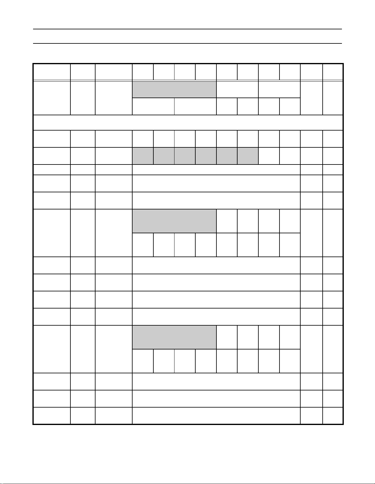
Philips Semiconductors Preliminary User Manual
LPC2114/2124/2212/2214ARM-based Microc ontroller
Table 2: LPC2114/2124/2212/2214 Registers
Address
Offset
0xE000403C T0EMR
TIMER1
0xE0008000 T1IR
0xE0008004 T1TCR
0xE0008008 T1TC T1 Counter 32 bit data RW 0
0xE000800C T1PR
0xE0008010 T1PC
0xE0008014 T1MCR
Name Description MSB LSB Access
T0 External
Match
Register
T1 Interrupt
Register
T1 Control
Register
T1 Prescale
Register
T1 Prescale
Counter
T1 Match
Control
Register
4 reserved (-) bits
External Match
Control 1
CR3
Int.
Reset
on
MR2
CR2
- - - - - -
4 reserved (-) bits
Int. on
MR2
Int.
External Match
Control 0
CR1
Int.
Stop
MR1
CR0
Reset
on
MR1
External Match
Control 3
Ext.
Mtch3.
MR3
Int.
32 bit data R/W 0
32 bit data R/W 0
on
Int.
Stop
on
MR3
Int. on
MR1
Mtch2.
MR2
Reset
MR3
Stop
MR0
Ext.
Int.
on
on
External Match
Control 2
Ext.
Mtch.1
MR1
Int.
CTR
Reset
Int. on
MR3
Reset
on
MR0
Ext.
Mtch.0
MR0
Int.
CTR
Enable
Stop
on
MR2
Int. on
MR0
R/W 0
R/W 0
R/W 0
R/W 0
Reset
Value
0xE0008018 T1MR0
0xE000801C T1MR1
0xE0008020 T1MR2
0xE0008024 T1MR3
0xE0008028 T1CCR
0xE000802C T1CR0
0xE0008030 T1CR1
0xE0008034 T1CR2
T1 Match
Register 0
T1 Match
Register 1
T1 Match
Register 2
T1 Match
Register 3
T1 Capture
Control
Register
T1 Capture
Register 0
T1 Capture
Register 1
T1 Capture
Register 2
4 reserved (-) bits
Int. on
Cpt.2
falling
Int. on
Cpt.2
rising
Int. on
Cpt.1
32 bit data R/W 0
32 bit data R/W 0
32 bit data R/W 0
32 bit data R/W 0
Int. on
Cpt.3
Int. on
Cpt.1
falling
Int. on
Cpt.1
rising
32 bit data RO 0
32 bit data RO 0
32 bit data RO 0
Int. on
Cpt.3
falling
Int. on
Cpt.0
Int. on
Cpt.3
rising
Int. on
Cpt.0
falling
Int. on
Cpt.2
R/W 0
Int. on
Cpt.0
rising
Introduction 22 May 03, 2004
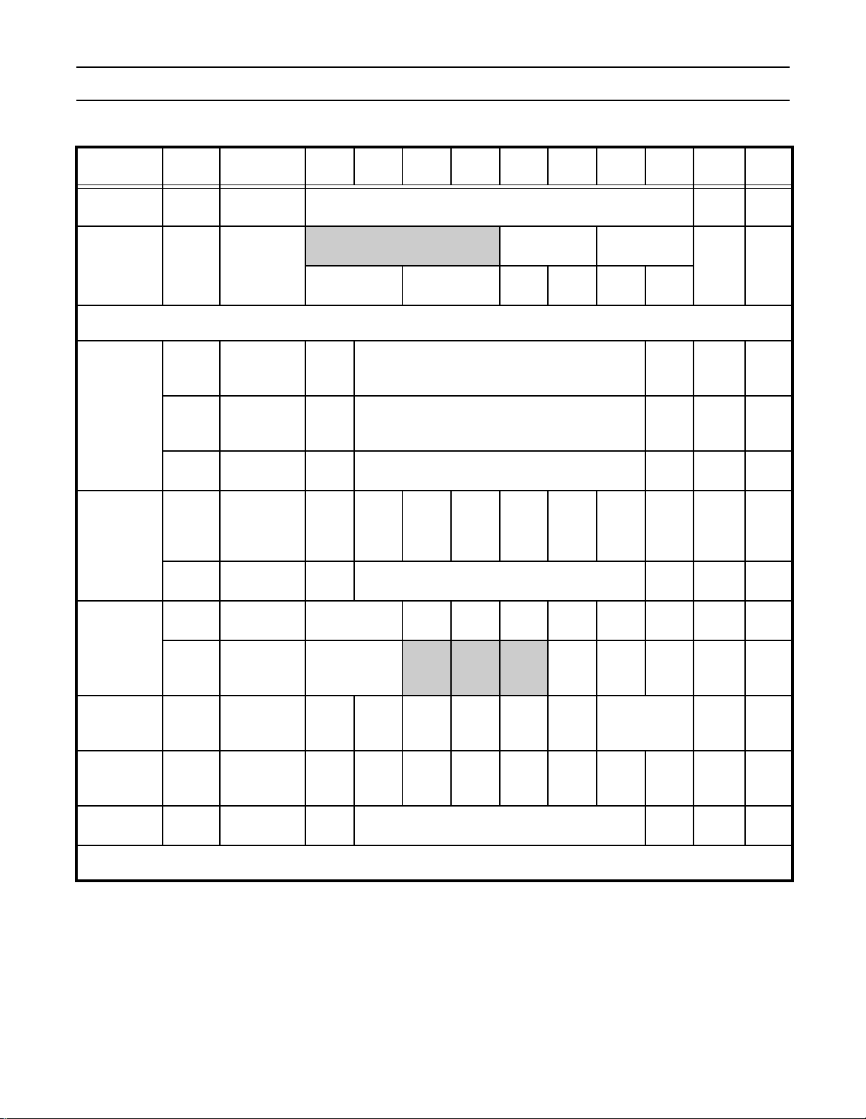
Philips Semiconductors Preliminary User Manual
LPC2114/2124/2212/2214ARM-based Microc ontroller
Table 2: LPC2114/2124/2212/2214 Registers
Address
Offset
Name Description MSB LSB Access
0xE0008038 T1CR3
0xE000803C T1EMR
UART0
U0RBR
(DLAB=0)
0xE000C000
U0THR
(DLAB=0)
U0DLL
(DLAB=1)
U0IER
0xE000C004
(DLAB=0)
T1 Capture
Register 3
T1 External
Match
Register
U0 Receiver
Buffer
Register
U0 Transmit
Holding
Register
U0 Divisor
Latch LSB
U0 Interrupt
Enable
Register
32 bit data RO 0
4 reserved (-) bits
External Match
Control 1
External Match
Control 0
External Match
Control 3
Ext.
Mtch.3
8 bit data RO
8 bit data WO NA
8 bit data R/W 0x01
00000
Ext.
Mtch2.
En. Rx
Line
Status
Int.
External Match
Control 2
Ext.
Mtch.1
Enable
THRE
Int.
Ext.
Mtch.0
En. Rx
Data
Av.Int.
Reset
Value
R/W 0
un-
defined
R/W 0
U0DLM
(DLAB=1)
U0IIR
0xE000C008
U0FCR
0xE000C00C U0LCR
0xE000C014 U0LSR
0xE000C01C U0SCR
UART1
U0 Divisor
Latch MSB
U0 Interrupt
ID Register
U0 FIFO
Control
Register
U0 Line
Control
Register
U0 Line
Status
Register
U0 Scratch
Pad Register
8 bit data R/W 0
FIFOs Enabled 0 0 IIR3 IIR2 IIR1 IIR0 RO 0x01
Rx Trigger
DLAB
Set
Break
- - -
Stick
Parity
Even
Parity
Select
Parity
Enable
U0 Tx
FIFO
Reset
Nm. of
Stop
Bits
U0 Rx
FIFO
Reset
U0
FIFO
Enable
Word Length
Select
WO 0
R/W 0
Rx
FIFO
TEMT THRE BI FE PE OE DR RO 0x60
Error
8 bit data R/W 0
Introduction 23 May 03, 2004

Philips Semiconductors Preliminary User Manual
LPC2114/2124/2212/2214ARM-based Microc ontroller
Table 2: LPC2114/2124/2212/2214 Registers
Address
Offset
Name Description MSB LSB Access
U1RBR
(DLAB=0)
0xE0010000
U1THR
(DLAB=0)
U1DLL
(DLAB=1)
U1IER
0xE0010004
(DLAB=0)
U1DLM
(DLAB=1)
U1IIR
0xE0010008
U1FCR
0xE001000C U1LCR
0xE0010010
U1
MCR
0xE0010014 U1LSR
U1 Receiver
Buffer
Register
U1 Transmit
Holding
Register
U1 Divisor
Latch LSB
U1 Interrupt
Enable
Register
U1 Divisor
Latch MSB
U1 Interrupt
ID Register
U1 FIFO
Control
Register
U1 Line
Control
Register
U1 Modem
Control
Register
U1 Line
Status
Register
Reset
Value
8 bit data RO
un-
defined
8 bit data WO NA
8 bit data R/W 0x01
En.
0000
Mdem
Satus
En. Rx
Status
Int.
Line
Int.
Enable
THRE
Int.
En. Rx
Data
Av.Int.
R/W 0
8 bit data R/W 0
FIFOs Enabled 0 0 IIR3 IIR2 IIR1 IIR0 RO 0x01
Rx Trigger
DLAB
Set
Break
- - -
Stick
Parity
000
Even
Parity
Select
Loop
Back
U0 Tx
FIFO
Reset
Parity
Enable
Nm. of
Stop
0 0 RTS DTR R/W 0
Bits
U0 Rx
FIFO
Reset
U0
FIFO
Enable
Word Length
Select
WO 0
R/W 0
Rx
FIFO
TEMT THRE BI FE PE OE DR RO 0x60
Error
U1
U1 Scratch
Pad Register
U1 Modem
Status
Register
8 bit data R/W 0
DCD RI DSR CTS
Delta
DCD
Trailing
Edge
RI
Delta
DSR
Delta
CTS
RO 0
0xE001001C U1SCR
0xE0010018
MSR
PWM
0xE0014000
0xE0014004
0xE0014008
IR
PWM
Interrupt
Register
PWM Timer
Control
Register
PWM
PWM
TCR
PWMTCPWM Timer
Counter
- - - - -
- - - -
- - - -
MR3
PWM
Enable
32 bit data RW 0
Int.
MR6
Int.
MR2
Int.
MR5
Int.
MR4
Int.
R/W 0
MR1
Int.
CTR
Reset
MR0
Int.
CTR
Enable
R/W 0
Introduction 24 May 03, 2004

Philips Semiconductors Preliminary User Manual
LPC2114/2124/2212/2214ARM-based Microc ontroller
Table 2: LPC2114/2124/2212/2214 Registers
Address
Offset
0xE001400C
0xE0014010
0xE0014014
0xE0014018
0xE001401C
0xE0014020
Name Description MSB LSB Access
PR
PC
PWM
Prescale
Register
PWM
Prescale
Counter
PWM Match
Control
Register
PWM Match
Register 0
PWM Match
Register 1
PWM Match
Register 2
11 reserved (-) bits
Int. on
MR5
Reset
on
MR2
Stop
on
MR4
Int. on
MR2
Reset
on
MR4
Stop
on
MR1
32 bit data R/W 0
32 bit data R/W 0
Stop
MR6
Int. on
MR4
Reset
MR1
on
on
Reset
on
MR6
Stop
on
MR3
Int. on
MR1
Int. on
MR6
Reset
on
MR3
Stop
on
MR0
Stop
on
MR5
Int. on
MR3
Reset
on
MR0
Reset
on
MR5
Stop
on
MR2
Int. on
MR0
R/W 0
32 bit data R/W 0
32 bit data R/W 0
32 bit data R/W 0
PWM
PWM
PWM
MCR
PWM
MR0
PWM
MR1
PWM
MR2
Reset
Value
0xE0014024
0xE0014040
0xE0014044
0xE0014048
0xE001404C
0xE0014050
2
C
I
0xE001C000
PWM
MR3
PWM
MR4
PWM
MR5
PWM
MR6
PWM
PCR
PWM
LER
I2CONSETI
0xE001C004 I2STAT
0xE001C008 I2DAT
PWM Match
Register 3
PWM Match
Register 4
PWM Match
Register 5
PWM Match
Register 6
PWM Control
Register
PWM Latch
Enable
Register
2
C Control
Set Register
2
C Status
I
Register
2
C Data
I
Register
32 bit data R/W 0
32 bit data R/W 0
32 bit data R/W 0
32 bit data R/W 0
- ENA6 ENA5 ENA4 ENA3 ENA2 ENA1 R/W 0
- SEL6 SEL5 SEL4 SEL3 SEL2 SEL1 -
Ena.
PWM
-
M6
Latch
Ena.
PWM
M5
Latch
Ena.
PWM
M4
Latch
Ena.
PWM
M3
Latch
Ena.
PWM
M2
Latch
Ena.
PWM
M1
Latch
Ena.
PWM
M0
Latch
R/W 0
-I2ENSTASTOSIAA - -R/W0
5 bit Status 0 0 0 RO 0xF8
8 bit data R/W 0
Introduction 25 May 03, 2004

Philips Semiconductors Preliminary User Manual
LPC2114/2124/2212/2214ARM-based Microc ontroller
Table 2: LPC2114/2124/2212/2214 Registers
Address
Offset
0xE001C00C
0xE001C010
0xE001C014
0xE001C018
SPI0
0xE0020000
0xE0020004
0xE0020008
0xE002000C
0xE002001C
Name Description MSB LSB Access
2
C Slave
I
I2
ADR
Address
Register
7 bit data GC R/W 0
SCL Duty
I2
SCLH
Cycle
Register High
16 bit data R/W 0x04
Half Word
SCL Duty
I2
SCLL
Cycle
Register Low
16 bit data R/W 0x04
Half Word
2
C Control
LR
S0
S0
S0
S0
S0
I
Clear
Register
SPI0 Control
Register
SPI0 Status
Register
SPI0 Data
Register
SPI0 Clock
Counter
Register
SPI0
Interrupt Flag
- I2ENC STAC - SIC AAC - -WONA
SPIE LSBF MSTR CPOL CPHA
SPIF WCOL ROVR MODF ABRT
- - -R/W0
- - -RO0
8 bit data R/W 0
8 bit data R/W 0
- - - - - - -
SPI
Int.
R/W 0
I2CONC
SPCR
SPSR
SPDR
SPCCR
SPINT
Reset
Value
SPI1
0xE0030000
0xE0030004
0xE0030008
0xE003000C
0xE003001C
SPCR
S1
SPSR
S1
SPDR
S1
SPCCR
S1
SPINT
SPI1 Control
Register
SPI1 Status
Register
SPI1 Data
Register
SPI1 Clock
Counter
Register
SPI1
Interrupt Flag
SPIE LSBF MSTR CPOL CPHA
SPIF WCOL ROVR MODF ABRT
8 bit data R/W 0
8 bit data R/W 0
- - - - - - -
- - -R/W0
- - -RO0
SPI
Int.
R/W 0
S1
RTC
Introduction 26 May 03, 2004
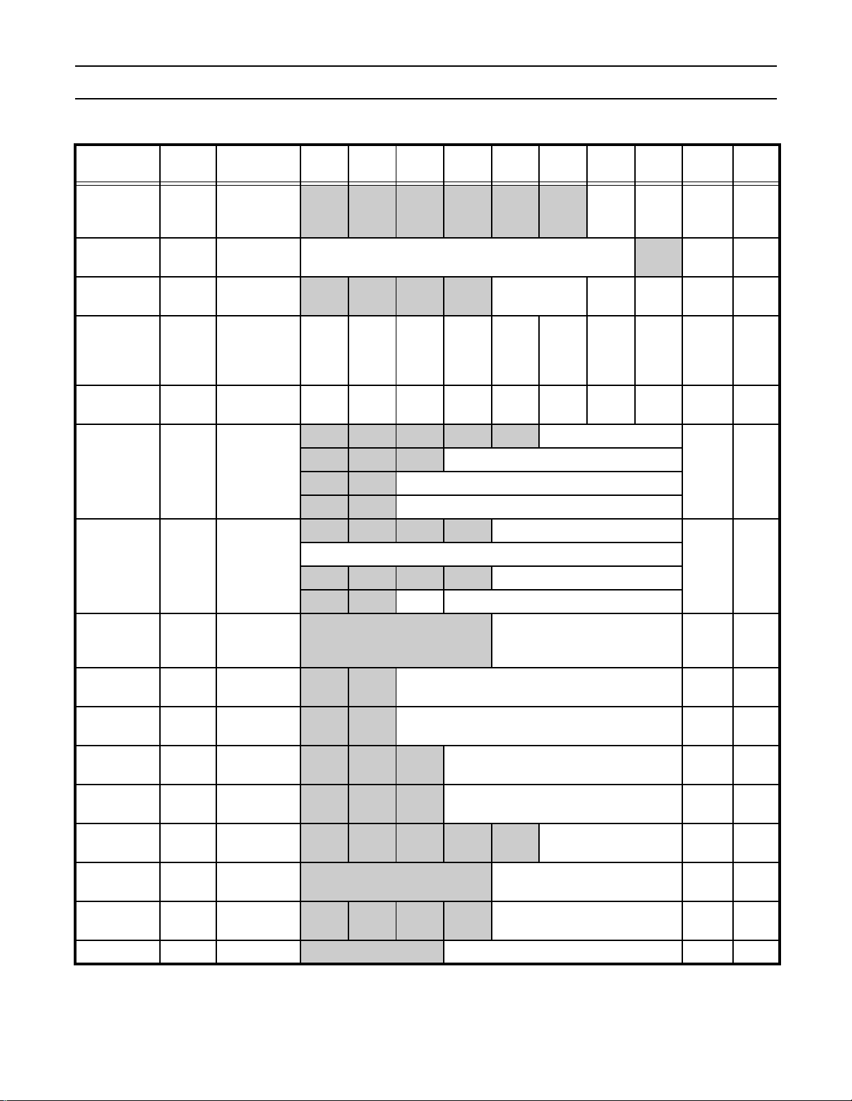
Philips Semiconductors Preliminary User Manual
LPC2114/2124/2212/2214ARM-based Microc ontroller
Table 2: LPC2114/2124/2212/2214 Registers
Address
Offset
Name Description MSB LSB Access
0xE0024000 ILR
0xE0024004 CTC
0xE0024008 CCR
0xE002400C CIIR
0xE0024010 AMR
0xE0024014
0xE0024018
CTIME0
CTIME1
Interrupt
Location
Register
Clock Tick
Counter
Clock Control
Register
Counter
Increment
Interrupt
Register
Alarm Mask
Register
Consolidated
Time
Register 0
Consolidated
Time
Register 1
- - - - - -
15 bit data
- - - - CTTEST
RTC
ALF
CTC
RST
RTC
CIF
-RO*
CLK
EN
IM
YEARIMMONIMDOYIMDOWIMDOMIMHOURIMMINIMSEC
AMR
YEAR
AMR
MON
AMR
DOY
AMR
DOW
AMR
DOM
AMR
HOUR
AMR
MIN
AMR
SEC
- - - - - 3 bit Day of Week
- - - 5 bit Hours
- - 6 bit Minutes
- - 6 bit Seconds
- - - 12 bit Year
- - - - 4 bit Month
- - - 5 bit Day of Month
Reset
Value
R/W *
R/W *
R/W *
R/W *
RO *
RO *
Consolidated
0xE002401C
CTIME2
Time
Register 2
0xE0024020 SEC
0xE0024024 MIN
0xE0024028 HOUR
0xE002402C DOM
0xE0024030 DOW
0xE0024034 DOY
0xE0024038
MONTH
Seconds
Register
Minutes
Register
Hours
Register
Day of Month
Register
Day of Week
Register
Day of Year
Register
Months
Register
0xE002403C YEAR Year Register
reserved (-) 20 bits 12 bit Day of Year RO *
- - 6 bit data R/W *
- - 6 bit data R/W *
- - - 5 bit data R/W *
- - - 5 bit data R/W *
- - - - - 3 bit data R/W *
reserved (-) 7 bits 9 bit data R/W *
- - - - 4 bit data R/W *
reserved (-) 4 bits 12 bit data R/W *
Introduction 27 May 03, 2004

Philips Semiconductors Preliminary User Manual
LPC2114/2124/2212/2214ARM-based Microc ontroller
Table 2: LPC2114/2124/2212/2214 Registers
Address
Offset
0xE0024060
0xE0024064
0xE0024068
0xE002406C
0xE0024070
0xE0024074
0xE0024078
0xE002407C
0xE0024080
0xE0024084
Name Description MSB LSB Access
AL
SEC
AL
MIN
AL
HOUR
AL
DOM
AL
DOW
AL
DOY
AL
MON
AL
YEAR
PRE
INT
PRE
FRAC
Alarm value
for Seconds
Alarm value
for Minutes
Alarm value
for Hours
Alarm value
for Day of
Month
Alarm value
for Day of
Week
Alarm value
for Day of
Year
Alarm value
for Months
Alarm value
for Year
Prescale
value, integer
portion
Prescale
value,
fractional
portion
- - 6 bit data R/W *
- - 6 bit data R/W *
- - - 5 bit data R/W *
- - - 5 bit data R/W *
- - - - - 3 bit data R/W *
reserved (-) 7 bits 9 bit data R/W *
- - - - 4 bit data R/W *
reserved
(-) 4 bits
reserved
(-) 3 bits
- 15 bit data R/W 0
12 bit data R/W *
13 bit data R/W 0
Reset
Value
GPIO PORT0
0xE0028000 IO0PIN
0xE0028004 IO0SET
0xE0028008 IO0DIR
0xE002800C IO0CLR
GPIO PORT1
0xE0028010 IO1PIN
0xE0028014 IO1SET
GPIO 0 Pin
Value reg.
GPIO 0 Out.
Set register
GPIO 0 Dir.
control reg.
GPIO 0 Out.
Clear register
GPIO 1 Pin
Value reg.
GPIO 1 Out.
Set register
32 bit data RO NA
32 bit data R/W 0
32 bit data R/W 0
32 bit data WO 0
32 bit data RO NA
32 bit data R/W 0
Introduction 28 May 03, 2004

Philips Semiconductors Preliminary User Manual
LPC2114/2124/2212/2214ARM-based Microc ontroller
Table 2: LPC2114/2124/2212/2214 Registers
Address
Offset
0xE0028018 IO1DIR
0xE002801C IO1CLR
GPIO PORT2
0xE0028020 IO2PIN
0xE0028024 IO2SET
0xE0028028 IO2DIR
0xE002802C IO2CLR
GPIO PORT3
0xE0028030 IO3PIN
0xE0028034 IO3SET
Name Description MSB LSB Access
GPIO 1 Dir.
control reg.
GPIO 1 Out.
Clear register
GPIO 2 Pin
Value reg.
GPIO 2 Out.
Set register
GPIO 2 Dir.
control reg.
GPIO 2 Out.
Clear register
GPIO 3 Pin
Value reg.
GPIO 3 Out.
Set register
Reset
Value
32 bit data R/W 0
32 bit data WO 0
32 bit data RO NA
32 bit data R/W 0
32 bit data R/W 0
32 bit data WO 0
32 bit data RO NA
32 bit data R/W 0
0xE0028038 IO3DIR
0xE002803C IO3CLR
Pin Connet Block
0xE002C000
0xE002C004
0xE002C014
ADC
PIN
SEL0
PIN
SEL1
PIN
SEL2
GPIO 3 Dir.
control reg.
GPIO 3 Out.
Clear register
Pin function
select
register 0
Pin function
select
register 1
Pin function
select
register 2
32 bit data R/W 0
32 bit data WO 0
32 bit data R/W 0
32 bit data R/W 0
-
24-bit pin configuration data (144 package case)
Reserved bits (64 package case)
configuration
data
R/W 0
-
Introduction 29 May 03, 2004
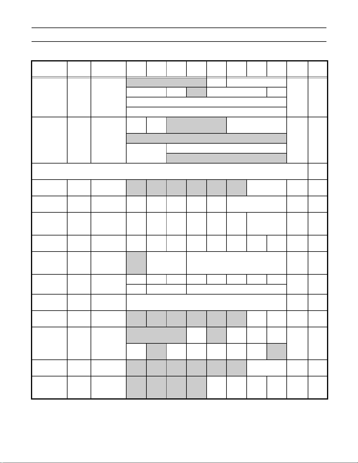
Philips Semiconductors Preliminary User Manual
LPC2114/2124/2212/2214ARM-based Microc ontroller
Table 2: LPC2114/2124/2212/2214 Registers
Address
Offset
Name Description MSB LSB Access
0xE0034000 ADCR ADC Control
register
0xE0034004 ADDR ADC Data
register
System Control Block
0xE01FC000
0xE01FC004
0xE01FC040
MAMCRMAM control
register
MAM
TIM
MEM
MAP
MAM timing
control
Memory
mapping
control
Reset
Value
- EDGE START
TEST1:0 PDN -CLKS
BURST
RW 01
8 bit data
8 bit data
DONE
OVER
RUN
- CHN
-
RW x
10 bit data
-
- - - - - - 2 bit data R/W 0
----- 3 bit data R/W0x07
------2 bit dataR/W0
0xE01FC080
0xE01FC084
0xE01FC088
0xE01FC08C
PLL
CON
PLL
CFG
PLL
STAT
PLL
FEED
0xE01FC0C0 PCON
0xE01FC0C4 PCONP
0xE01FC100
0xE01FC140
VPB
DIV
EXT
INT
PLL control
register
PLL
configuration
register
PLL status
register
PLL feed
register
Power control
register
Power control
for
peripherals
VPB divider
control
External
interrupt flag
register
------PLLCPLLER/W0
- 2bit data PSEL 5 bit data MSEL R/W 0
-----
PLOCK
PLLC PLLE
RO 0
- 2bit data PSEL 5 bit data MSEL
8 bit data WO NA
- - - - - - PD IDL R/W 0
reserved (-) 19 bits PCAD -
PC
SPI1PCRTCPCSPI0
R/W 0x3BE
PC
I2C
PC
PWM0PCURT1PCURT0PCTIM1PCTIM0
-
- - - - - - 2 bit data R/W 0
- - - - EINT3 EINT2 EINT1 EINT0 R/W 0
Introduction 30 May 03, 2004
 Loading...