

Page 1

INTEGRATED CIRCUITS
LPC2131/2132/2138
User Manual
Preliminary Release
November 22, 2004
Philips
Semiconductors
PHILIPS
Page 2

P
hilips Semiconductors Preliminary User Manu
al
LPC2131/2132/2138ARM-based Microc ontroller
2 November 22, 2004
Page 3

P
hilips Semiconductors Preliminary User Manu
al
LPC2131/2132/2138ARM-based Micr ocontroller
Table of Contents
List of Figures . . . . . . . . . . . . . . . . . . . . . . . . . . . . . . . . . . . . . . . . . . . . . . . . . . . . . . . . . . . . . . . . . 7
List of Tables . . . . . . . . . . . . . . . . . . . . . . . . . . . . . . . . . . . . . . . . . . . . . . . . . . . . . . . . . . . . . . . . . . 9
Document Revision History . . . . . . . . . . . . . . . . . . . . . . . . . . . . . . . . . . . . . . . . . . . . . . . . . . . . . . 13
Introduction . . . . . . . . . . . . . . . . . . . . . . . . . . . . . . . . . . . . . . . . . . . . . . . . . . . . . . . . . . . . 15
General Description . . . . . . . . . . . . . . . . . . . . . . . . . . . . . . . . . . . . . . . . . . . . . . . . . . . . . . . . . . . . 15
Features . . . . . . . . . . . . . . . . . . . . . . . . . . . . . . . . . . . . . . . . . . . . . . . . . . . . . . . . . . . . . . . . . . . . . 15
Applications . . . . . . . . . . . . . . . . . . . . . . . . . . . . . . . . . . . . . . . . . . . . . . . . . . . . . . . . . . . . . . . . . . 16
Device information . . . . . . . . . . . . . . . . . . . . . . . . . . . . . . . . . . . . . . . . . . . . . . . . . . . . . . . . . . . . . 16
Architectural Overview . . . . . . . . . . . . . . . . . . . . . . . . . . . . . . . . . . . . . . . . . . . . . . . . . . . . . . . . . . 17
ARM7TDMI-S Processor . . . . . . . . . . . . . . . . . . . . . . . . . . . . . . . . . . . . . . . . . . . . . . . . . . . . . . . . 17
On-Chip Flash Memory System . . . . . . . . . . . . . . . . . . . . . . . . . . . . . . . . . . . . . . . . . . . . . . . . . . . 17
On-Chip Static RAM . . . . . . . . . . . . . . . . . . . . . . . . . . . . . . . . . . . . . . . . . . . . . . . . . . . . . . . . . . . . 18
Block Diagram . . . . . . . . . . . . . . . . . . . . . . . . . . . . . . . . . . . . . . . . . . . . . . . . . . . . . . . . . . . . . . . . 19
LPC2131/2132/2138 Memory Addressing . . . . . . . . . . . . . . . . . . . . . . . . . . . . . . . . . . . . 21
Memory Maps . . . . . . . . . . . . . . . . . . . . . . . . . . . . . . . . . . . . . . . . . . . . . . . . . . . . . . . . . . . . . . . . 21
LPC2131/2132/2138 Memory Re-mapping and Boot Block . . . . . . . . . . . . . . . . . . . . . . . . . . . . . 25
Prefetch Abort and Data Abort Exceptions . . . . . . . . . . . . . . . . . . . . . . . . . . . . . . . . . . . . . . . . . . 28
System Control Block . . . . . . . . . . . . . . . . . . . . . . . . . . . . . . . . . . . . . . . . . . . . . . . . . . . . 29
Summary of System Control Block Functions . . . . . . . . . . . . . . . . . . . . . . . . . . . . . . . . . . . . . . . . 29
Pin Description . . . . . . . . . . . . . . . . . . . . . . . . . . . . . . . . . . . . . . . . . . . . . . . . . . . . . . . . . . . . . . . . 29
Register Description . . . . . . . . . . . . . . . . . . . . . . . . . . . . . . . . . . . . . . . . . . . . . . . . . . . . . . . . . . . . 30
Crystal Oscillator . . . . . . . . . . . . . . . . . . . . . . . . . . . . . . . . . . . . . . . . . . . . . . . . . . . . . . . . . . . . . . 31
External Interrupt Inputs . . . . . . . . . . . . . . . . . . . . . . . . . . . . . . . . . . . . . . . . . . . . . . . . . . . . . . . . . 33
Memory Mapping Control . . . . . . . . . . . . . . . . . . . . . . . . . . . . . . . . . . . . . . . . . . . . . . . . . . . . . . . . 38
PLL (Phase Locked Loop) . . . . . . . . . . . . . . . . . . . . . . . . . . . . . . . . . . . . . . . . . . . . . . . . . . . . . . . 39
Power Control . . . . . . . . . . . . . . . . . . . . . . . . . . . . . . . . . . . . . . . . . . . . . . . . . . . . . . . . . . . . . . . . 45
Reset . . . . . . . . . . . . . . . . . . . . . . . . . . . . . . . . . . . . . . . . . . . . . . . . . . . . . . . . . . . . . . . . . . . . . . . 47
VPB Divider . . . . . . . . . . . . . . . . . . . . . . . . . . . . . . . . . . . . . . . . . . . . . . . . . . . . . . . . . . . . . . . . . . 49
Wakeup Timer . . . . . . . . . . . . . . . . . . . . . . . . . . . . . . . . . . . . . . . . . . . . . . . . . . . . . . . . . . . . . . . . 51
Brown-out Detection . . . . . . . . . . . . . . . . . . . . . . . . . . . . . . . . . . . . . . . . . . . . . . . . . . . . . . . . . . . 52
Code Security vs. Debugging . . . . . . . . . . . . . . . . . . . . . . . . . . . . . . . . . . . . . . . . . . . . . . . . . . . . 53
Memory Accelerator Module (MAM) . . . . . . . . . . . . . . . . . . . . . . . . . . . . . . . . . . . . . . . . 55
Introduction . . . . . . . . . . . . . . . . . . . . . . . . . . . . . . . . . . . . . . . . . . . . . . . . . . . . . . . . . . . . . . . . . . 55
Operation . . . . . . . . . . . . . . . . . . . . . . . . . . . . . . . . . . . . . . . . . . . . . . . . . . . . . . . . . . . . . . . . . . . . 55
Memory Accelerator Module Operating Modes . . . . . . . . . . . . . . . . . . . . . . . . . . . . . . . . . . . . . . . 57
MAM Configuration . . . . . . . . . . . . . . . . . . . . . . . . . . . . . . . . . . . . . . . . . . . . . . . . . . . . . . . . . . . . 58
Register Description . . . . . . . . . . . . . . . . . . . . . . . . . . . . . . . . . . . . . . . . . . . . . . . . . . . . . . . . . . . . 58
MAM Usage Notes . . . . . . . . . . . . . . . . . . . . . . . . . . . . . . . . . . . . . . . . . . . . . . . . . . . . . . . . . . . . . 59
Vectored Interrupt Controller (VIC) . . . . . . . . . . . . . . . . . . . . . . . . . . . . . . . . . . . . . . . . . 61
Features . . . . . . . . . . . . . . . . . . . . . . . . . . . . . . . . . . . . . . . . . . . . . . . . . . . . . . . . . . . . . . . . . . . . . 61
Description . . . . . . . . . . . . . . . . . . . . . . . . . . . . . . . . . . . . . . . . . . . . . . . . . . . . . . . . . . . . . . . . . . . 61
Register Description . . . . . . . . . . . . . . . . . . . . . . . . . . . . . . . . . . . . . . . . . . . . . . . . . . . . . . . . . . . . 62
VIC Registers . . . . . . . . . . . . . . . . . . . . . . . . . . . . . . . . . . . . . . . . . . . . . . . . . . . . . . . . . . . . . . . . . 64
Interrupt Sources . . . . . . . . . . . . . . . . . . . . . . . . . . . . . . . . . . . . . . . . . . . . . . . . . . . . . . . . . . . . . . 68
Spurious Interrupts . . . . . . . . . . . . . . . . . . . . . . . . . . . . . . . . . . . . . . . . . . . . . . . . . . . . . . . . . . . . . 71
VIC Usage Notes . . . . . . . . . . . . . . . . . . . . . . . . . . . . . . . . . . . . . . . . . . . . . . . . . . . . . . . . . . . . . . 74
3 November 22, 2004
Page 4

P
hilips Semiconductors Preliminary User Manu
al
LPC2131/2132/2138ARM-based Micr ocontroller
Pin Configuration . . . . . . . . . . . . . . . . . . . . . . . . . . . . . . . . . . . . . . . . . . . . . . . . . . . . . . . 75
LPC2131/2132/2138 Pinout . . . . . . . . . . . . . . . . . . . . . . . . . . . . . . . . . . . . . . . . . . . . . . . . . . . . . . 75
Pin Description for LPC2131/2132/2138 . . . . . . . . . . . . . . . . . . . . . . . . . . . . . . . . . . . . . . . . . . . . 76
Pin Connect Block . . . . . . . . . . . . . . . . . . . . . . . . . . . . . . . . . . . . . . . . . . . . . . . . . . . . . . . 81
Features . . . . . . . . . . . . . . . . . . . . . . . . . . . . . . . . . . . . . . . . . . . . . . . . . . . . . . . . . . . . . . . . . . . . . 81
Applications . . . . . . . . . . . . . . . . . . . . . . . . . . . . . . . . . . . . . . . . . . . . . . . . . . . . . . . . . . . . . . . . . . 81
Description . . . . . . . . . . . . . . . . . . . . . . . . . . . . . . . . . . . . . . . . . . . . . . . . . . . . . . . . . . . . . . . . . . . 81
Register Description . . . . . . . . . . . . . . . . . . . . . . . . . . . . . . . . . . . . . . . . . . . . . . . . . . . . . . . . . . . . 81
GPIO . . . . . . . . . . . . . . . . . . . . . . . . . . . . . . . . . . . . . . . . . . . . . . . . . . . . . . . . . . . . . . . . . . 85
Features . . . . . . . . . . . . . . . . . . . . . . . . . . . . . . . . . . . . . . . . . . . . . . . . . . . . . . . . . . . . . . . . . . . . . 85
Applications . . . . . . . . . . . . . . . . . . . . . . . . . . . . . . . . . . . . . . . . . . . . . . . . . . . . . . . . . . . . . . . . . . 85
Pin Description . . . . . . . . . . . . . . . . . . . . . . . . . . . . . . . . . . . . . . . . . . . . . . . . . . . . . . . . . . . . . . . . 85
Register Description . . . . . . . . . . . . . . . . . . . . . . . . . . . . . . . . . . . . . . . . . . . . . . . . . . . . . . . . . . . . 85
GPIO Usage Notes . . . . . . . . . . . . . . . . . . . . . . . . . . . . . . . . . . . . . . . . . . . . . . . . . . . . . . . . . . . . 88
UART0 . . . . . . . . . . . . . . . . . . . . . . . . . . . . . . . . . . . . . . . . . . . . . . . . . . . . . . . . . . . . . . . . . 89
Features . . . . . . . . . . . . . . . . . . . . . . . . . . . . . . . . . . . . . . . . . . . . . . . . . . . . . . . . . . . . . . . . . . . . . 89
Pin Description . . . . . . . . . . . . . . . . . . . . . . . . . . . . . . . . . . . . . . . . . . . . . . . . . . . . . . . . . . . . . . . . 89
Register Description . . . . . . . . . . . . . . . . . . . . . . . . . . . . . . . . . . . . . . . . . . . . . . . . . . . . . . . . . . . . 90
Architecture . . . . . . . . . . . . . . . . . . . . . . . . . . . . . . . . . . . . . . . . . . . . . . . . . . . . . . . . . . . . . . . . . . 99
UART1 . . . . . . . . . . . . . . . . . . . . . . . . . . . . . . . . . . . . . . . . . . . . . . . . . . . . . . . . . . . . . . . . 101
Features . . . . . . . . . . . . . . . . . . . . . . . . . . . . . . . . . . . . . . . . . . . . . . . . . . . . . . . . . . . . . . . . . . . . 101
Pin Description . . . . . . . . . . . . . . . . . . . . . . . . . . . . . . . . . . . . . . . . . . . . . . . . . . . . . . . . . . . . . . . 101
Register Description . . . . . . . . . . . . . . . . . . . . . . . . . . . . . . . . . . . . . . . . . . . . . . . . . . . . . . . . . . . 102
Architecture . . . . . . . . . . . . . . . . . . . . . . . . . . . . . . . . . . . . . . . . . . . . . . . . . . . . . . . . . . . . . . . . . 113
I2C Interfaces I2C0 and I2C1 . . . . . . . . . . . . . . . . . . . . . . . . . . . . . . . . . . . . . . . . . . . . . 115
Features . . . . . . . . . . . . . . . . . . . . . . . . . . . . . . . . . . . . . . . . . . . . . . . . . . . . . . . . . . . . . . . . . . . . 115
Applications . . . . . . . . . . . . . . . . . . . . . . . . . . . . . . . . . . . . . . . . . . . . . . . . . . . . . . . . . . . . . . . . . 115
Description . . . . . . . . . . . . . . . . . . . . . . . . . . . . . . . . . . . . . . . . . . . . . . . . . . . . . . . . . . . . . . . . . . 115
Pin Description . . . . . . . . . . . . . . . . . . . . . . . . . . . . . . . . . . . . . . . . . . . . . . . . . . . . . . . . . . . . . . . 116
I2C Operating Modes . . . . . . . . . . . . . . . . . . . . . . . . . . . . . . . . . . . . . . . . . . . . . . . . . . . . . . . . . . 116
I2C Implementation and Operation . . . . . . . . . . . . . . . . . . . . . . . . . . . . . . . . . . . . . . . . . . . . . . . 119
Register Description . . . . . . . . . . . . . . . . . . . . . . . . . . . . . . . . . . . . . . . . . . . . . . . . . . . . . . . . . . . 123
Details of I2C Operating Modes . . . . . . . . . . . . . . . . . . . . . . . . . . . . . . . . . . . . . . . . . . . . . . . . . . 128
Software Example . . . . . . . . . . . . . . . . . . . . . . . . . . . . . . . . . . . . . . . . . . . . . . . . . . . . . . . . . . . . 144
SPI Interface (SPI0) . . . . . . . . . . . . . . . . . . . . . . . . . . . . . . . . . . . . . . . . . . . . . . . . . . . . . 153
Features . . . . . . . . . . . . . . . . . . . . . . . . . . . . . . . . . . . . . . . . . . . . . . . . . . . . . . . . . . . . . . . . . . . . 153
Description . . . . . . . . . . . . . . . . . . . . . . . . . . . . . . . . . . . . . . . . . . . . . . . . . . . . . . . . . . . . . . . . . . 153
Pin Description . . . . . . . . . . . . . . . . . . . . . . . . . . . . . . . . . . . . . . . . . . . . . . . . . . . . . . . . . . . . . . . 157
Register Description . . . . . . . . . . . . . . . . . . . . . . . . . . . . . . . . . . . . . . . . . . . . . . . . . . . . . . . . . . . 158
Architecture . . . . . . . . . . . . . . . . . . . . . . . . . . . . . . . . . . . . . . . . . . . . . . . . . . . . . . . . . . . . . . . . . 161
SSP Controller (SPI1) . . . . . . . . . . . . . . . . . . . . . . . . . . . . . . . . . . . . . . . . . . . . . . . . . . . 163
Features . . . . . . . . . . . . . . . . . . . . . . . . . . . . . . . . . . . . . . . . . . . . . . . . . . . . . . . . . . . . . . . . . . . . 163
Description . . . . . . . . . . . . . . . . . . . . . . . . . . . . . . . . . . . . . . . . . . . . . . . . . . . . . . . . . . . . . . . . . . 163
Pin Descriptions . . . . . . . . . . . . . . . . . . . . . . . . . . . . . . . . . . . . . . . . . . . . . . . . . . . . . . . . . . . . . . 163
Texas Instruments Synchronous Serial Frame Format . . . . . . . . . . . . . . . . . . . . . . . . . . . . . . . . 164
SPI Frame Format . . . . . . . . . . . . . . . . . . . . . . . . . . . . . . . . . . . . . . . . . . . . . . . . . . . . . . . . . . . . 165
Semiconductor Microwire Frame Format . . . . . . . . . . . . . . . . . . . . . . . . . . . . . . . . . . . . . . . . . . . 169
Register Descriptions . . . . . . . . . . . . . . . . . . . . . . . . . . . . . . . . . . . . . . . . . . . . . . . . . . . . . . . . . . 171
4 November 22, 2004
Page 5

P
hilips Semiconductors Preliminary User Manu
al
LPC2131/2132/2138ARM-based Micr ocontroller
Timer/Counter0 and Timer/Counter1 . . . . . . . . . . . . . . . . . . . . . . . . . . . . . . . . . . . . . . . 175
Features . . . . . . . . . . . . . . . . . . . . . . . . . . . . . . . . . . . . . . . . . . . . . . . . . . . . . . . . . . . . . . . . . . . . 175
Applications . . . . . . . . . . . . . . . . . . . . . . . . . . . . . . . . . . . . . . . . . . . . . . . . . . . . . . . . . . . . . . . . . 175
Description . . . . . . . . . . . . . . . . . . . . . . . . . . . . . . . . . . . . . . . . . . . . . . . . . . . . . . . . . . . . . . . . . . 176
Pin Description . . . . . . . . . . . . . . . . . . . . . . . . . . . . . . . . . . . . . . . . . . . . . . . . . . . . . . . . . . . . . . . 176
Register Description . . . . . . . . . . . . . . . . . . . . . . . . . . . . . . . . . . . . . . . . . . . . . . . . . . . . . . . . . . . 177
Example Timer Operation . . . . . . . . . . . . . . . . . . . . . . . . . . . . . . . . . . . . . . . . . . . . . . . . . . . . . . 183
Architecture . . . . . . . . . . . . . . . . . . . . . . . . . . . . . . . . . . . . . . . . . . . . . . . . . . . . . . . . . . . . . . . . . 184
Pulse Width Modulator (PWM) . . . . . . . . . . . . . . . . . . . . . . . . . . . . . . . . . . . . . . . . . . . . 185
Features . . . . . . . . . . . . . . . . . . . . . . . . . . . . . . . . . . . . . . . . . . . . . . . . . . . . . . . . . . . . . . . . . . . . 185
Description . . . . . . . . . . . . . . . . . . . . . . . . . . . . . . . . . . . . . . . . . . . . . . . . . . . . . . . . . . . . . . . . . . 185
Pin Description . . . . . . . . . . . . . . . . . . . . . . . . . . . . . . . . . . . . . . . . . . . . . . . . . . . . . . . . . . . . . . . 190
Register Description . . . . . . . . . . . . . . . . . . . . . . . . . . . . . . . . . . . . . . . . . . . . . . . . . . . . . . . . . . . 191
A/D Converter . . . . . . . . . . . . . . . . . . . . . . . . . . . . . . . . . . . . . . . . . . . . . . . . . . . . . . . . . 197
Features . . . . . . . . . . . . . . . . . . . . . . . . . . . . . . . . . . . . . . . . . . . . . . . . . . . . . . . . . . . . . . . . . . . . 197
Description . . . . . . . . . . . . . . . . . . . . . . . . . . . . . . . . . . . . . . . . . . . . . . . . . . . . . . . . . . . . . . . . . . 197
Pin DescriptionS . . . . . . . . . . . . . . . . . . . . . . . . . . . . . . . . . . . . . . . . . . . . . . . . . . . . . . . . . . . . . 198
Register Description . . . . . . . . . . . . . . . . . . . . . . . . . . . . . . . . . . . . . . . . . . . . . . . . . . . . . . . . . . . 198
OPERATION . . . . . . . . . . . . . . . . . . . . . . . . . . . . . . . . . . . . . . . . . . . . . . . . . . . . . . . . . . . . . . . . 201
D/A Converter (LPC2132/2138 only) . . . . . . . . . . . . . . . . . . . . . . . . . . . . . . . . . . . . . . . 203
Features . . . . . . . . . . . . . . . . . . . . . . . . . . . . . . . . . . . . . . . . . . . . . . . . . . . . . . . . . . . . . . . . . . . . 203
Pin DescriptionS . . . . . . . . . . . . . . . . . . . . . . . . . . . . . . . . . . . . . . . . . . . . . . . . . . . . . . . . . . . . . 203
Register Description . . . . . . . . . . . . . . . . . . . . . . . . . . . . . . . . . . . . . . . . . . . . . . . . . . . . . . . . . . . 203
OPERATION . . . . . . . . . . . . . . . . . . . . . . . . . . . . . . . . . . . . . . . . . . . . . . . . . . . . . . . . . . . . . . . . 203
Real Time Clock . . . . . . . . . . . . . . . . . . . . . . . . . . . . . . . . . . . . . . . . . . . . . . . . . . . . . . . . 205
Features . . . . . . . . . . . . . . . . . . . . . . . . . . . . . . . . . . . . . . . . . . . . . . . . . . . . . . . . . . . . . . . . . . . . 205
Description . . . . . . . . . . . . . . . . . . . . . . . . . . . . . . . . . . . . . . . . . . . . . . . . . . . . . . . . . . . . . . . . . . 205
Architecture . . . . . . . . . . . . . . . . . . . . . . . . . . . . . . . . . . . . . . . . . . . . . . . . . . . . . . . . . . . . . . . . . 206
Register Description . . . . . . . . . . . . . . . . . . . . . . . . . . . . . . . . . . . . . . . . . . . . . . . . . . . . . . . . . . . 206
RTC Interrupts . . . . . . . . . . . . . . . . . . . . . . . . . . . . . . . . . . . . . . . . . . . . . . . . . . . . . . . . . . . . . . . 208
Miscellaneous Register Group . . . . . . . . . . . . . . . . . . . . . . . . . . . . . . . . . . . . . . . . . . . . . . . . . . . 209
Consolidated Time Registers . . . . . . . . . . . . . . . . . . . . . . . . . . . . . . . . . . . . . . . . . . . . . . . . . . . . 212
Time Counter Group . . . . . . . . . . . . . . . . . . . . . . . . . . . . . . . . . . . . . . . . . . . . . . . . . . . . . . . . . . 214
Alarm Register Group . . . . . . . . . . . . . . . . . . . . . . . . . . . . . . . . . . . . . . . . . . . . . . . . . . . . . . . . . 215
RTC Usage Notes . . . . . . . . . . . . . . . . . . . . . . . . . . . . . . . . . . . . . . . . . . . . . . . . . . . . . . . . . . . . 215
Reference Clock Divider (Prescaler) . . . . . . . . . . . . . . . . . . . . . . . . . . . . . . . . . . . . . . . . . . . . . . 216
Watchdog . . . . . . . . . . . . . . . . . . . . . . . . . . . . . . . . . . . . . . . . . . . . . . . . . . . . . . . . . . . . . 219
Features . . . . . . . . . . . . . . . . . . . . . . . . . . . . . . . . . . . . . . . . . . . . . . . . . . . . . . . . . . . . . . . . . . . . 219
Applications . . . . . . . . . . . . . . . . . . . . . . . . . . . . . . . . . . . . . . . . . . . . . . . . . . . . . . . . . . . . . . . . . 219
Description . . . . . . . . . . . . . . . . . . . . . . . . . . . . . . . . . . . . . . . . . . . . . . . . . . . . . . . . . . . . . . . . . . 219
Register Description . . . . . . . . . . . . . . . . . . . . . . . . . . . . . . . . . . . . . . . . . . . . . . . . . . . . . . . . . . . 220
Block Diagram . . . . . . . . . . . . . . . . . . . . . . . . . . . . . . . . . . . . . . . . . . . . . . . . . . . . . . . . . . . . . . . 223
5 November 22, 2004
Page 6

P
hilips Semiconductors Preliminary User Manu
al
LPC2131/2132/2138ARM-based Micr ocontroller
Flash Memory System and Programming . . . . . . . . . . . . . . . . . . . . . . . . . . . . . . . . . . . 225
Flash Boot Loader . . . . . . . . . . . . . . . . . . . . . . . . . . . . . . . . . . . . . . . . . . . . . . . . . . . . . . . . . . . . 225
Features . . . . . . . . . . . . . . . . . . . . . . . . . . . . . . . . . . . . . . . . . . . . . . . . . . . . . . . . . . . . . . . . . . . . 225
Applications . . . . . . . . . . . . . . . . . . . . . . . . . . . . . . . . . . . . . . . . . . . . . . . . . . . . . . . . . . . . . . . . . 225
Description . . . . . . . . . . . . . . . . . . . . . . . . . . . . . . . . . . . . . . . . . . . . . . . . . . . . . . . . . . . . . . . . . . 225
Boot process FlowChart . . . . . . . . . . . . . . . . . . . . . . . . . . . . . . . . . . . . . . . . . . . . . . . . . . . . . . . . 228
Sector Numbers . . . . . . . . . . . . . . . . . . . . . . . . . . . . . . . . . . . . . . . . . . . . . . . . . . . . . . . . . . . . . . 229
fLASH cONTENT pROTECTION mECHANISM . . . . . . . . . . . . . . . . . . . . . . . . . . . . . . . . . . . . . 230
Code Read Protection . . . . . . . . . . . . . . . . . . . . . . . . . . . . . . . . . . . . . . . . . . . . . . . . . . . . . . . . . 230
IAP Commands . . . . . . . . . . . . . . . . . . . . . . . . . . . . . . . . . . . . . . . . . . . . . . . . . . . . . . . . . . . . . . 238
JTAG Flash Programming interface . . . . . . . . . . . . . . . . . . . . . . . . . . . . . . . . . . . . . . . . . . . . . . . 244
EmbeddedICE Logic . . . . . . . . . . . . . . . . . . . . . . . . . . . . . . . . . . . . . . . . . . . . . . . . . . . . 245
Features . . . . . . . . . . . . . . . . . . . . . . . . . . . . . . . . . . . . . . . . . . . . . . . . . . . . . . . . . . . . . . . . . . . . 245
Applications . . . . . . . . . . . . . . . . . . . . . . . . . . . . . . . . . . . . . . . . . . . . . . . . . . . . . . . . . . . . . . . . . 245
Description . . . . . . . . . . . . . . . . . . . . . . . . . . . . . . . . . . . . . . . . . . . . . . . . . . . . . . . . . . . . . . . . . . 245
Pin Description . . . . . . . . . . . . . . . . . . . . . . . . . . . . . . . . . . . . . . . . . . . . . . . . . . . . . . . . . . . . . . . 246
Reset State of Multiplexed Pins . . . . . . . . . . . . . . . . . . . . . . . . . . . . . . . . . . . . . . . . . . . . . . . . . . 246
Register Description . . . . . . . . . . . . . . . . . . . . . . . . . . . . . . . . . . . . . . . . . . . . . . . . . . . . . . . . . . . 247
Block Diagram . . . . . . . . . . . . . . . . . . . . . . . . . . . . . . . . . . . . . . . . . . . . . . . . . . . . . . . . . . . . . . . 248
Embedded Trace Macrocell . . . . . . . . . . . . . . . . . . . . . . . . . . . . . . . . . . . . . . . . . . . . . . 249
Features . . . . . . . . . . . . . . . . . . . . . . . . . . . . . . . . . . . . . . . . . . . . . . . . . . . . . . . . . . . . . . . . . . . . 249
Applications . . . . . . . . . . . . . . . . . . . . . . . . . . . . . . . . . . . . . . . . . . . . . . . . . . . . . . . . . . . . . . . . . 249
Description . . . . . . . . . . . . . . . . . . . . . . . . . . . . . . . . . . . . . . . . . . . . . . . . . . . . . . . . . . . . . . . . . . 249
Pin Description . . . . . . . . . . . . . . . . . . . . . . . . . . . . . . . . . . . . . . . . . . . . . . . . . . . . . . . . . . . . . . . 250
Reset State of Multiplexed Pins . . . . . . . . . . . . . . . . . . . . . . . . . . . . . . . . . . . . . . . . . . . . . . . . . . 250
Register Description . . . . . . . . . . . . . . . . . . . . . . . . . . . . . . . . . . . . . . . . . . . . . . . . . . . . . . . . . . . 251
Block Diagram . . . . . . . . . . . . . . . . . . . . . . . . . . . . . . . . . . . . . . . . . . . . . . . . . . . . . . . . . . . . . . . 252
RealMonitor . . . . . . . . . . . . . . . . . . . . . . . . . . . . . . . . . . . . . . . . . . . . . . . . . . . . . . . . . . . 253
Features . . . . . . . . . . . . . . . . . . . . . . . . . . . . . . . . . . . . . . . . . . . . . . . . . . . . . . . . . . . . . . . . . . . . 253
Applications . . . . . . . . . . . . . . . . . . . . . . . . . . . . . . . . . . . . . . . . . . . . . . . . . . . . . . . . . . . . . . . . . 253
Description . . . . . . . . . . . . . . . . . . . . . . . . . . . . . . . . . . . . . . . . . . . . . . . . . . . . . . . . . . . . . . . . . . 253
How to Enable RealMonitor . . . . . . . . . . . . . . . . . . . . . . . . . . . . . . . . . . . . . . . . . . . . . . . . . . . . . 257
RealMonitor build options . . . . . . . . . . . . . . . . . . . . . . . . . . . . . . . . . . . . . . . . . . . . . . . . . . . . . . 263
6 November 22, 2004
Page 7

P
hilips Semiconductors Preliminary User Manu
al
LPC2131/2132/2138ARM-based Micr ocontroller
List of Figures
Figure 1: LPC2131/2132/2138 Block Diagram . . . . . . . . . . . . . . . . . . . . . . . . . . . . . . . . . . . . . . . . . . . . . 19
Figure 2: System Memory Map . . . . . . . . . . . . . . . . . . . . . . . . . . . . . . . . . . . . . . . . . . . . . . . . . . . . . . . . . 21
Figure 3: Peripheral Memory Map. . . . . . . . . . . . . . . . . . . . . . . . . . . . . . . . . . . . . . . . . . . . . . . . . . . . . . . 22
Figure 4: AHB Peripheral Map. . . . . . . . . . . . . . . . . . . . . . . . . . . . . . . . . . . . . . . . . . . . . . . . . . . . . . . . . . 23
Figure 5: VPB Peripheral Map. . . . . . . . . . . . . . . . . . . . . . . . . . . . . . . . . . . . . . . . . . . . . . . . . . . . . . . . . . 24
Figure 6: Map of lower memory is showing re-mapped and re-mappable areas
(LPC2138 with 512 kB Flash). . . . . . . . . . . . . . . . . . . . . . . . . . . . . . . . . . . . . . . . . . . . . . . . . . . 27
Figure 7: Oscillator modes and models: a) slave mode of operation, b) oscillation mode of operation,
c) external crystal model used for CX1/X2 evaluation . . . . . . . . . . . . . . . . . . . . . . . . . . . . . . . . 31
Figure 8: FOSC selection algorithm. . . . . . . . . . . . . . . . . . . . . . . . . . . . . . . . . . . . . . . . . . . . . . . . . . . . . . 32
Figure 9: External Interrupt Logic. . . . . . . . . . . . . . . . . . . . . . . . . . . . . . . . . . . . . . . . . . . . . . . . . . . . . . . . 37
Figure 10: PLL Block Diagram. . . . . . . . . . . . . . . . . . . . . . . . . . . . . . . . . . . . . . . . . . . . . . . . . . . . . . . . . . . 40
Figure 11: Reset Block Diagram including Wakeup Timer . . . . . . . . . . . . . . . . . . . . . . . . . . . . . . . . . . . . . 48
Figure 12: VPB Divider Connections. . . . . . . . . . . . . . . . . . . . . . . . . . . . . . . . . . . . . . . . . . . . . . . . . . . . . . 50
Figure 13: Simplified Block Diagram of the Memory Accelerator Module . . . . . . . . . . . . . . . . . . . . . . . . . . 56
Figure 14: Block Diagram of the Vectored Interrupt Controller . . . . . . . . . . . . . . . . . . . . . . . . . . . . . . . . . . 69
Figure 15: LPC2131/2132/2138 64-pin package. . . . . . . . . . . . . . . . . . . . . . . . . . . . . . . . . . . . . . . . . . . . . 75
Figure 16: LPC2131/2132/2138 UART0 Block Diagram . . . . . . . . . . . . . . . . . . . . . . . . . . . . . . . . . . . . . . 100
Figure 17: UART1 Block Diagram . . . . . . . . . . . . . . . . . . . . . . . . . . . . . . . . . . . . . . . . . . . . . . . . . . . . . . . 114
Figure 18: I2C Bus Configuration. . . . . . . . . . . . . . . . . . . . . . . . . . . . . . . . . . . . . . . . . . . . . . . . . . . . . . . . 116
Figure 19: Master Mode Configuration . . . . . . . . . . . . . . . . . . . . . . . . . . . . . . . . . . . . . . . . . . . . . . . . . . . 117
Figure 20: Format in the master transmitter mode. . . . . . . . . . . . . . . . . . . . . . . . . . . . . . . . . . . . . . . . . . . 117
Figure 21: Format of master receiver mode. . . . . . . . . . . . . . . . . . . . . . . . . . . . . . . . . . . . . . . . . . . . . . . . 118
Figure 22: A master receiver switch to master transmitter after sending repeated START. . . . . . . . . . . . 118
Figure 23: Slave Mode Configuration . . . . . . . . . . . . . . . . . . . . . . . . . . . . . . . . . . . . . . . . . . . . . . . . . . . . 118
Figure 24: Format of slave receiver mode. . . . . . . . . . . . . . . . . . . . . . . . . . . . . . . . . . . . . . . . . . . . . . . . . 119
Figure 25: Format of slave transmitter mode. . . . . . . . . . . . . . . . . . . . . . . . . . . . . . . . . . . . . . . . . . . . . . . 119
Figure 26: I2C Bus Serial Interface Block Diagram . . . . . . . . . . . . . . . . . . . . . . . . . . . . . . . . . . . . . . . . . . 120
Figure 27: Arbitration Procedure . . . . . . . . . . . . . . . . . . . . . . . . . . . . . . . . . . . . . . . . . . . . . . . . . . . . . . . . 121
Figure 28: Serial Clock Synchronization (Figure 14). . . . . . . . . . . . . . . . . . . . . . . . . . . . . . . . . . . . . . . . . 122
Figure 29: (Format and States in the Master Transmitter Mode . . . . . . . . . . . . . . . . . . . . . . . . . . . . . . . . 131
Figure 30: Format and States in the Master Receiver Mode. . . . . . . . . . . . . . . . . . . . . . . . . . . . . . . . . . . 132
Figure 31: Format and States in the Slave Receiver Mode. . . . . . . . . . . . . . . . . . . . . . . . . . . . . . . . . . . . 133
Figure 32: Format and States of the Slave Transmitter Mode. . . . . . . . . . . . . . . . . . . . . . . . . . . . . . . . . . 134
Figure 33: Simultaneous Repeated START Conditions from 2 Masters . . . . . . . . . . . . . . . . . . . . . . . . . . 141
Figure 34: Forced Access to a Busy I2C Bus . . . . . . . . . . . . . . . . . . . . . . . . . . . . . . . . . . . . . . . . . . . . . . 142
Figure 35: Recovering from a Bus Obstruction Caused by a Low Level on SDA . . . . . . . . . . . . . . . . . . . 142
Figure 36: SPI Data Transfer Format (CPHA = 0 and CPHA = 1). . . . . . . . . . . . . . . . . . . . . . . . . . . . . . . 154
Figure 37: SPI Block Diagram . . . . . . . . . . . . . . . . . . . . . . . . . . . . . . . . . . . . . . . . . . . . . . . . . . . . . . . . . . 161
Figure 38: Texas Instruments synchronous serial frame format:
a) single and b) continuous/back-to-back two frames transfer. . . . . . . . . . . . . . . . . . . . . . . . . 164
Figure 39: SPI frame format with CPOL=0 and CPHA=0 (a) single and b) continuous transfer) . . . . . . . 165
Figure 40: SPI frame format with CPOL=0 and CPHA=1 . . . . . . . . . . . . . . . . . . . . . . . . . . . . . . . . . . . . . 166
Figure 41: SPI frame format with CPOL=1 and CPHA=0 (a) single and b) continuous transfer) . . . . . . . 167
Figure 42: SPI frame format with CPOL=1 and CPHA=1 . . . . . . . . . . . . . . . . . . . . . . . . . . . . . . . . . . . . . 168
Figure 43: Microwire frame format (single transfer). . . . . . . . . . . . . . . . . . . . . . . . . . . . . . . . . . . . . . . . . . 169
Figure 44: Microwire frame format (continuos transfers). . . . . . . . . . . . . . . . . . . . . . . . . . . . . . . . . . . . . . 170
Figure 45: Microwire frame format (continuos transfers). . . . . . . . . . . . . . . . . . . . . . . . . . . . . . . . . . . . . . 170
Figure 46: A timer cycle in which PR=2, MRx=6, and both interrupt and reset on match are enabled.. . . 183
Figure 47: A timer cycle in which PR=2, MRx=6, and both interrupt and stop on match are enabled. . . . 183
Figure 48: Timer block diagram. . . . . . . . . . . . . . . . . . . . . . . . . . . . . . . . . . . . . . . . . . . . . . . . . . . . . . . . . 184
Figure 49: PWM block diagram . . . . . . . . . . . . . . . . . . . . . . . . . . . . . . . . . . . . . . . . . . . . . . . . . . . . . . . . . 187
Figure 50: Sample PWM waveforms. . . . . . . . . . . . . . . . . . . . . . . . . . . . . . . . . . . . . . . . . . . . . . . . . . . . . 188
Figure 51: RTC block diagram. . . . . . . . . . . . . . . . . . . . . . . . . . . . . . . . . . . . . . . . . . . . . . . . . . . . . . . . . . 206
Figure 52: RTC Prescaler block diagram. . . . . . . . . . . . . . . . . . . . . . . . . . . . . . . . . . . . . . . . . . . . . . . . . . 217
7 November 22, 2004
Page 8

P
hilips Semiconductors Preliminary User Manu
al
LPC2131/2132/2138ARM-based Micr ocontroller
Figure 53: Watchdog Block Diagram. . . . . . . . . . . . . . . . . . . . . . . . . . . . . . . . . . . . . . . . . . . . . . . . . . . . . 223
Figure 54: Map of lower memory after reset . . . . . . . . . . . . . . . . . . . . . . . . . . . . . . . . . . . . . . . . . . . . . . . 226
Figure 55: Boot Process flowchart. . . . . . . . . . . . . . . . . . . . . . . . . . . . . . . . . . . . . . . . . . . . . . . . . . . . . . . 228
Figure 56: IAP Parameter passing. . . . . . . . . . . . . . . . . . . . . . . . . . . . . . . . . . . . . . . . . . . . . . . . . . . . . . . 240
Figure 57: EmbeddedICE Debug Environment Block Diagram. . . . . . . . . . . . . . . . . . . . . . . . . . . . . . . . . 248
Figure 58: ETM Debug Environment Block Diagram. . . . . . . . . . . . . . . . . . . . . . . . . . . . . . . . . . . . . . . . . 252
Figure 59: RealMonitor components . . . . . . . . . . . . . . . . . . . . . . . . . . . . . . . . . . . . . . . . . . . . . . . . . . . . . 254
Figure 60: RealMonitor as a state machine. . . . . . . . . . . . . . . . . . . . . . . . . . . . . . . . . . . . . . . . . . . . . . . . 255
Figure 61: Exception Handlers. . . . . . . . . . . . . . . . . . . . . . . . . . . . . . . . . . . . . . . . . . . . . . . . . . . . . . . . . . 258
8 November 22, 2004
Page 9

P
hilips Semiconductors Preliminary User Manu
al
LPC2131/2132/2138ARM-based Micr ocontroller
List of Tables
Table 1: LPC2131/2132/2138 device information . . . . . . . . . . . . . . . . . . . . . . . . . . . . . . . . . . . . . . . . . . . 16
Table 2: ARM Exception Vector Locations. . . . . . . . . . . . . . . . . . . . . . . . . . . . . . . . . . . . . . . . . . . . . . . . . 25
Table 3: LPC2131/2132/2138 Memory Mapping Modes . . . . . . . . . . . . . . . . . . . . . . . . . . . . . . . . . . . . . . 25
Table 4: Pin summary . . . . . . . . . . . . . . . . . . . . . . . . . . . . . . . . . . . . . . . . . . . . . . . . . . . . . . . . . . . . . . . . 29
Table 5: Summary of System Control Registers . . . . . . . . . . . . . . . . . . . . . . . . . . . . . . . . . . . . . . . . . . . . 30
Table 6: Recommended values for CX1/X2 in oscillation mode
(crystal and external components parameters) . . . . . . . . . . . . . . . . . . . . . . . . . . . . . . . . . . . . . . 31
Table 7: External Interrupt Registers. . . . . . . . . . . . . . . . . . . . . . . . . . . . . . . . . . . . . . . . . . . . . . . . . . . . . 33
Table 8: External Interrupt Flag Register (EXTINT - 0xE01FC140). . . . . . . . . . . . . . . . . . . . . . . . . . . . . . 34
Table 9: Interrupt Wakeup Register (INTWAKE - 0xE01FC144). . . . . . . . . . . . . . . . . . . . . . . . . . . . . . . . 35
Table 10: External Interrupt Mode Register (EXTMODE - 0xE01FC148) . . . . . . . . . . . . . . . . . . . . . . . . . . 35
Table 11: External Interrupt Polarity Register (EXTPOLAR - 0xE01FC14C). . . . . . . . . . . . . . . . . . . . . . . . 36
Table 12: MEMMAP Register. . . . . . . . . . . . . . . . . . . . . . . . . . . . . . . . . . . . . . . . . . . . . . . . . . . . . . . . . . . . 38
Table 13: Memory Mapping Control Register (MEMMAP - 0xE01FC040). . . . . . . . . . . . . . . . . . . . . . . . . . 38
Table 14: PLL Registers. . . . . . . . . . . . . . . . . . . . . . . . . . . . . . . . . . . . . . . . . . . . . . . . . . . . . . . . . . . . . . . . 39
Table 15: PLL Control Register (PLLCON - 0xE01FC080) . . . . . . . . . . . . . . . . . . . . . . . . . . . . . . . . . . . . . 41
Table 16: PLL Configuration Register (PLLCFG - 0xE01FC084) . . . . . . . . . . . . . . . . . . . . . . . . . . . . . . . . 41
Table 17: PLL Status Register (PLLSTAT - 0xE01FC088) . . . . . . . . . . . . . . . . . . . . . . . . . . . . . . . . . . . . . 42
Table 18: PLL Control Bit Combinations . . . . . . . . . . . . . . . . . . . . . . . . . . . . . . . . . . . . . . . . . . . . . . . . . . . 42
Table 19: PLL Feed Register (PLLFEED - 0xE01FC08C). . . . . . . . . . . . . . . . . . . . . . . . . . . . . . . . . . . . . . 43
Table 20: PLL Divider Values. . . . . . . . . . . . . . . . . . . . . . . . . . . . . . . . . . . . . . . . . . . . . . . . . . . . . . . . . . . . 44
Table 21: PLL Multiplier Values. . . . . . . . . . . . . . . . . . . . . . . . . . . . . . . . . . . . . . . . . . . . . . . . . . . . . . . . . . 44
Table 22: Power Control Registers . . . . . . . . . . . . . . . . . . . . . . . . . . . . . . . . . . . . . . . . . . . . . . . . . . . . . . . 45
Table 23: Power Control Register (PCON - 0xE01FC0C0). . . . . . . . . . . . . . . . . . . . . . . . . . . . . . . . . . . . . 46
Table 24: Power Control for Peripherals Register for LPC2131/2132/2138 (PCONP - 0xE01FC0C4). . . . 46
Table 25: Power Control for Peripherals Register for LPC2131/2132/2138 (PCONP - 0xE01FC0C4). . . . 49
Table 26: VPBDIV Register Map . . . . . . . . . . . . . . . . . . . . . . . . . . . . . . . . . . . . . . . . . . . . . . . . . . . . . . . . . 49
Table 27: VPB Divider Register (VPBDIV - 0xE01FC100). . . . . . . . . . . . . . . . . . . . . . . . . . . . . . . . . . . . . . 50
Table 28: MAM Responses to Program Accesses of Various Types. . . . . . . . . . . . . . . . . . . . . . . . . . . . . . 57
Table 29: MAM Responses to Data and DMA Accesses of Various Types. . . . . . . . . . . . . . . . . . . . . . . . . 57
Table 30: Summary of System Control Registers . . . . . . . . . . . . . . . . . . . . . . . . . . . . . . . . . . . . . . . . . . . . 58
Table 31: MAM Control Register (MAMCR - 0xE01FC000). . . . . . . . . . . . . . . . . . . . . . . . . . . . . . . . . . . . . 59
Table 32: MAM Timing Register (MAMTIM - 0xE01FC004) . . . . . . . . . . . . . . . . . . . . . . . . . . . . . . . . . . . . 59
Table 33: VIC Register Map. . . . . . . . . . . . . . . . . . . . . . . . . . . . . . . . . . . . . . . . . . . . . . . . . . . . . . . . . . . . . 62
Table 34: Software Interrupt Register (VICSoftInt - 0xFFFFF018, Read/Write) . . . . . . . . . . . . . . . . . . . . . 64
Table 35: Software Interrupt Clear Register (VICSoftIntClear - 0xFFFFF01C, Write Only). . . . . . . . . . . . . 64
Table 36: Raw Interrupt Status Register (VICRawIntr - 0xFFFFF008, Read-Only). . . . . . . . . . . . . . . . . . . 64
Table 37: Interrupt Enable Register (VICINtEnable - 0xFFFFF010, Read/Write) . . . . . . . . . . . . . . . . . . . . 65
Table 38: Software Interrupt Clear Register (VICIntEnClear - 0xFFFFF014, Write Only) . . . . . . . . . . . . . . 65
Table 39: Interrupt Select Register (VICIntSelect - 0xFFFFF00C, Read/Write) . . . . . . . . . . . . . . . . . . . . . 65
Table 40: IRQ Status Register (VICIRQStatus - 0xFFFFF000, Read-Only) . . . . . . . . . . . . . . . . . . . . . . . . 65
Table 41: IRQ Status Register (VICFIQStatus - 0xFFFFF004, Read-Only) . . . . . . . . . . . . . . . . . . . . . . . . 66
Table 42: Vector Control Registers (VICVectCntl0-15 - 0xFFFFF200-23C, Read/Write) . . . . . . . . . . . . . . 66
Table 43: Vector Address Registers (VICVectAddr0-15 - 0xFFFFF100-13C, Read/Write). . . . . . . . . . . . . 66
Table 44: Default Vector Address Register (VICDefVectAddr - 0xFFFFF034, Read/Write) . . . . . . . . . . . . 66
Table 45: Vector Address Register (VICVectAddr - 0xFFFFF030, Read/Write). . . . . . . . . . . . . . . . . . . . . 67
Table 46: Protection Enable Register (VICProtection - 0xFFFFF020, Read/Write). . . . . . . . . . . . . . . . . . . 67
Table 47: Connection of Interrupt Sources to the Vectored Interrupt Controller . . . . . . . . . . . . . . . . . . . . . 68
Table 48: Pin description for LPC2131/2132/2138 . . . . . . . . . . . . . . . . . . . . . . . . . . . . . . . . . . . . . . . . . . . 76
Table 49: Pin Connect Block Register Map . . . . . . . . . . . . . . . . . . . . . . . . . . . . . . . . . . . . . . . . . . . . . . . . . 81
Table 50: Pin Function Select Register 0 (PINSEL0 - 0xE002C000). . . . . . . . . . . . . . . . . . . . . . . . . . . . . . 82
Table 51: Pin Function Select Register 1 (PINSEL1 - 0xE002C004). . . . . . . . . . . . . . . . . . . . . . . . . . . . . . 82
Table 52: Pin Function Select Register 2 (PINSEL2 - 0xE002C014). . . . . . . . . . . . . . . . . . . . . . . . . . . . . . 83
Table 53: Pin Function Select Register Bits. . . . . . . . . . . . . . . . . . . . . . . . . . . . . . . . . . . . . . . . . . . . . . . . . 84
Table 54: GPIO Pin Description. . . . . . . . . . . . . . . . . . . . . . . . . . . . . . . . . . . . . . . . . . . . . . . . . . . . . . . . . . 85
9 November 22, 2004
Page 10

P
hilips Semiconductors Preliminary User Manu
al
LPC2131/2132/2138ARM-based Micr ocontroller
Table 55: GPIO Register Map . . . . . . . . . . . . . . . . . . . . . . . . . . . . . . . . . . . . . . . . . . . . . . . . . . . . . . . . . . . 86
Table 56: GPIO Pin Value Register (IO0PIN - 0xE0028000, IO1PIN - 0xE0028010) . . . . . . . . . . . . . . . . . 87
Table 57: GPIO Output Set Register (IO0SET - 0xE0028004, IO1SET - 0xE0028014) . . . . . . . . . . . . . . . 87
Table 58: GPIO Output Clear Register (IO0CLR - 0xE002800C, IO1CLR - 0xE002801C). . . . . . . . . . . . . 87
Table 59: GPIO Direction Register (IO0DIR - 0xE0028008, IO1DIR - 0xE0028018) . . . . . . . . . . . . . . . . . 88
Table 60: UART0 Pin Description . . . . . . . . . . . . . . . . . . . . . . . . . . . . . . . . . . . . . . . . . . . . . . . . . . . . . . . . 89
Table 61: UART0 Register Map. . . . . . . . . . . . . . . . . . . . . . . . . . . . . . . . . . . . . . . . . . . . . . . . . . . . . . . . . . 90
Table 62: UART0 Receiver Buffer Register (U0RBR - 0xE000C000 when DLAB = 0, Read Only). . . . . . . 91
Table 63: UART0 Transmitter Holding Register (U0THR - 0xE000C000 when DLAB = 0, Write Only) . . . 91
Table 64: UART0 Divisor Latch LSB Register (U0DLL - 0xE000C000 when DLAB = 1). . . . . . . . . . . . . . . 91
Table 65: UART0 Divisor Latch MSB Register (U0DLM - 0xE000C004 when DLAB = 1). . . . . . . . . . . . . . 92
Table 66: UART0 Interrupt Enable Register (U0IER - 0xE000C004 when DLAB = 0) . . . . . . . . . . . . . . . . 92
Table 67: UART0 Interrupt Identification Register (U0IIR - 0xE000C008, Read Only) . . . . . . . . . . . . . . . . 93
Table 68: UART0 Interrupt Handling . . . . . . . . . . . . . . . . . . . . . . . . . . . . . . . . . . . . . . . . . . . . . . . . . . . . . . 94
Table 69: UART0 FIFO Control Register (U0FCR - 0xE000C008) . . . . . . . . . . . . . . . . . . . . . . . . . . . . . . . 94
Table 70: UART0 Line Control Register (U0LCR - 0xE000C00C). . . . . . . . . . . . . . . . . . . . . . . . . . . . . . . . 95
Table 71: UART0 Line Status Register (U0LSR - 0xE000C014, Read Only) . . . . . . . . . . . . . . . . . . . . . . . 96
Table 72: UART0 Scratch Pad Register (U0SCR - 0xE000C01C) . . . . . . . . . . . . . . . . . . . . . . . . . . . . . . . 97
Table 73: Baud-rates using 20 MHz peripheral clock (pclk). . . . . . . . . . . . . . . . . . . . . . . . . . . . . . . . . . . . . 97
Table 74: UART0 Transmit Enable Register (U0TER - 0xE0010030). . . . . . . . . . . . . . . . . . . . . . . . . . . . . 98
Table 75: UART1 Pin Description . . . . . . . . . . . . . . . . . . . . . . . . . . . . . . . . . . . . . . . . . . . . . . . . . . . . . . . 101
Table 76: UART1 Register Map. . . . . . . . . . . . . . . . . . . . . . . . . . . . . . . . . . . . . . . . . . . . . . . . . . . . . . . . . 102
Table 77: UART1 Receiver Buffer Register (U1RBR - 0xE0010000 when DLAB = 0, Read Only). . . . . . 103
Table 78: UART1 Transmitter Holding Register (U1THR - 0xE0010000 when DLAB = 0, Write Only) . . . 103
Table 79: UART1 Divisor Latch LSB Register (U1DLL - 0xE0010000 when DLAB = 1) . . . . . . . . . . . . . . 104
Table 80: UART1 Divisor Latch MSB Register (U1DLM - 0xE0010004 when DLAB = 1). . . . . . . . . . . . . 104
Table 81: UART1 Interrupt Enable Register (U1IER - 0xE0010004 when DLAB = 0). . . . . . . . . . . . . . . . 104
Table 82: UART1 Interrupt Identification Register (U1IIR - 0xE0010008, Read Only) . . . . . . . . . . . . . . . 105
Table 83: UART1 Interrupt Handling . . . . . . . . . . . . . . . . . . . . . . . . . . . . . . . . . . . . . . . . . . . . . . . . . . . . . 106
Table 84: UART1 FIFO Control Register (U1FCR - 0xE0010008) . . . . . . . . . . . . . . . . . . . . . . . . . . . . . . 107
Table 85: UART1 Line Control Register (U1LCR - 0xE001000C) . . . . . . . . . . . . . . . . . . . . . . . . . . . . . . . 107
Table 86: UART1 Modem Control Register (U1MCR - 0xE0010010) (LPC2138 only) . . . . . . . . . . . . . . . 108
Table 87: UART1 Line Status Register (U1LSR - 0xE0010014, Read Only). . . . . . . . . . . . . . . . . . . . . . . 108
Table 88: UART1 Modem Status Register Bit Descriptions (U1MSR - 0x0xE0010018) (LPC2138 only) . 110
Table 89: UART1 Scratch Pad Register (U1SCR - 0xE001001C). . . . . . . . . . . . . . . . . . . . . . . . . . . . . . . 110
Table 90: Baud-rates using 20 MHz peripheral clock (pclk). . . . . . . . . . . . . . . . . . . . . . . . . . . . . . . . . . . . 111
Table 91: UART1 Transmit Enable Register (U1TER - 0xE0010030). . . . . . . . . . . . . . . . . . . . . . . . . . . . 112
Table 92: I2C Pin Description . . . . . . . . . . . . . . . . . . . . . . . . . . . . . . . . . . . . . . . . . . . . . . . . . . . . . . . . . . 116
Table 93: I2C Register Map. . . . . . . . . . . . . . . . . . . . . . . . . . . . . . . . . . . . . . . . . . . . . . . . . . . . . . . . . . . . 123
Table 94: I2C Control Set Register
(I2CONSET: I2C0 - I2C0CONSET: 0xE001C000; I2C1 - I2C1CONSET: 0xE005C000) . . . . . 124
Table 95: I2C Control Clear Register
(I2CONCLR: I2C0 - I2C0CONCLR: 0xE001C018; I2C1 - I2C1CONCLR: 0xE005C018) . . . . . 125
Table 96: I2C Status Register
(I2STAT: I2C0 - I2C0STAT: 0xE001C004; I2C1 - I2C1STAT: 0xE005C004) . . . . . . . . . . . . . . 126
Table 97: I2C Data Register (I2DAT: I2C0 - I2C0DAT: 0xE001C008; I2C1 - I2C1DAT: 0xE005C008) . . 126
Table 98: I2C Slave Address Register
(I2ADR: I2C0 - I2C0DAT: 0xE001C00C; I2C1 - I2C1DAT: 0xE005C00C) . . . . . . . . . . . . . . . . 126
Table 99: I2C SCL High Duty Cycle Register
(I2SCLH: I2C0 - I2C0SCLH: 0xE001C010; I2C1 - I2C1SCLH: 0xE005C010). . . . . . . . . . . . . . 127
Table 100: I2C SCL Low Duty Cycle Register
(I2SCLL: I2C0 - I2C0SCLL: 0xE001C014; I2C1 - I2C1SCLL: 0xE005C014) . . . . . . . . . . . . . . 127
Table 101: Example I2C Clock Rates . . . . . . . . . . . . . . . . . . . . . . . . . . . . . . . . . . . . . . . . . . . . . . . . . . . . . 127
Table 102: Master Transmitter Mode . . . . . . . . . . . . . . . . . . . . . . . . . . . . . . . . . . . . . . . . . . . . . . . . . . . . . 135
Table 103: Master Receiver Mode . . . . . . . . . . . . . . . . . . . . . . . . . . . . . . . . . . . . . . . . . . . . . . . . . . . . . . . 136
Table 104: Slave Receiver Mode . . . . . . . . . . . . . . . . . . . . . . . . . . . . . . . . . . . . . . . . . . . . . . . . . . . . . . . . 137
Table 105: Slave Transmitter Mode . . . . . . . . . . . . . . . . . . . . . . . . . . . . . . . . . . . . . . . . . . . . . . . . . . . . . . 139
10 November 22, 2004
Page 11

P
hilips Semiconductors Preliminary User Manu
al
LPC2131/2132/2138ARM-based Micr ocontroller
Table 106: Miscellaneous States . . . . . . . . . . . . . . . . . . . . . . . . . . . . . . . . . . . . . . . . . . . . . . . . . . . . . . . . 140
Table 107: SPI Data To Clock Phase Relationship. . . . . . . . . . . . . . . . . . . . . . . . . . . . . . . . . . . . . . . . . . . 154
Table 108: SPI Pin Description. . . . . . . . . . . . . . . . . . . . . . . . . . . . . . . . . . . . . . . . . . . . . . . . . . . . . . . . . . 157
Table 109: SPI Register Map . . . . . . . . . . . . . . . . . . . . . . . . . . . . . . . . . . . . . . . . . . . . . . . . . . . . . . . . . . . 158
Table 110: SPI Control Register (S0SPCR - 0xE0020000). . . . . . . . . . . . . . . . . . . . . . . . . . . . . . . . . . . . . 158
Table 111: SPI Status Register (S0SPSR - 0xE0020004) . . . . . . . . . . . . . . . . . . . . . . . . . . . . . . . . . . . . . 159
Table 112: SPI Data Register (S0SPDR - 0xE0020008). . . . . . . . . . . . . . . . . . . . . . . . . . . . . . . . . . . . . . . 159
Table 113: SPI Clock Counter Register (S0SPCCR - 0xE002000C) . . . . . . . . . . . . . . . . . . . . . . . . . . . . . 159
Table 114: SPI Interrupt Register (S0SPINT - 0xE002001C) . . . . . . . . . . . . . . . . . . . . . . . . . . . . . . . . . . . 160
Table 115: SSP Pin Descriptions . . . . . . . . . . . . . . . . . . . . . . . . . . . . . . . . . . . . . . . . . . . . . . . . . . . . . . . . 163
Table 116: SSP Registers. . . . . . . . . . . . . . . . . . . . . . . . . . . . . . . . . . . . . . . . . . . . . . . . . . . . . . . . . . . . . . 171
Table 117: SSP Control Register 0 (SSPCR0 - 0xE0068000) . . . . . . . . . . . . . . . . . . . . . . . . . . . . . . . . . . 171
Table 118: SSP Control Register 1 (SSPCR1 - 0xE0068004) . . . . . . . . . . . . . . . . . . . . . . . . . . . . . . . . . . 172
Table 119: SSP Data Register (SSPDR - 0xE0068008). . . . . . . . . . . . . . . . . . . . . . . . . . . . . . . . . . . . . . . 172
Table 120: SSP Status Register (SSPSR - 0xE006800C) . . . . . . . . . . . . . . . . . . . . . . . . . . . . . . . . . . . . . 173
Table 121: SSP Clock Prescale Register (SSPCPSR - 0xE0068010) . . . . . . . . . . . . . . . . . . . . . . . . . . . . 173
Table 122: SSP Interrupt Mask Set/Clear Register (SSPIMSC - 0xE0068014) . . . . . . . . . . . . . . . . . . . . . 173
Table 123: SSP Raw Interrupt Status Register (SSPRIS - 0xE0068018). . . . . . . . . . . . . . . . . . . . . . . . . . 174
Table 124: SSP Masked Interrupt Status Register (SSPMIS - 0xE006801C). . . . . . . . . . . . . . . . . . . . . . . 174
Table 125: SSP Interrupt Clear Register (SSPICR - 0xE0068020). . . . . . . . . . . . . . . . . . . . . . . . . . . . . . . 174
Table 126: Pin summary. . . . . . . . . . . . . . . . . . . . . . . . . . . . . . . . . . . . . . . . . . . . . . . . . . . . . . . . . . . . . . . 176
Table 127: TIMER0 and TIMER1 Register Map . . . . . . . . . . . . . . . . . . . . . . . . . . . . . . . . . . . . . . . . . . . . . 177
Table 128: Interrupt Register (IR: TIMER0 - T0IR: 0xE0004000; TIMER1 - T1IR: 0xE0008000). . . . . . . . 178
Table 129: Timer Control Register
(TCR: TIMER0 - T0TCR: 0xE0004004; TIMER1 - T1TCR: 0xE0008004). . . . . . . . . . . . . . . . . 178
Table 130: Count Control Register
(CTCR: TIMER0 - T0CTCR: 0xE0004070; TIMER1 - T1TCR: 0xE0008070) . . . . . . . . . . . . . . 179
Table 131: Match Control Register
(MCR: TIMER0 - T0MCR: 0xE0004014; TIMER1 - T1MCR: 0xE0008014). . . . . . . . . . . . . . . . 180
Table 132: Capture Control Register
(CCR: TIMER0 - T0CCR: 0xE0004028; TIMER1 - T1CCR: 0xE0008028) . . . . . . . . . . . . . . . . 180
Table 133: External Match Register
(EMR: TIMER0 - T0EMR: 0xE000403C; TIMER1 - T1EMR: 0xE000803C) . . . . . . . . . . . . . . . 181
Table 134: External Match Control . . . . . . . . . . . . . . . . . . . . . . . . . . . . . . . . . . . . . . . . . . . . . . . . . . . . . . . 182
Table 135: Set and Reset inputs for PWM Flip-Flops. . . . . . . . . . . . . . . . . . . . . . . . . . . . . . . . . . . . . . . . . 188
Table 136: Pin summary. . . . . . . . . . . . . . . . . . . . . . . . . . . . . . . . . . . . . . . . . . . . . . . . . . . . . . . . . . . . . . . 190
Table 137: Pulse Width Modulator Register Map . . . . . . . . . . . . . . . . . . . . . . . . . . . . . . . . . . . . . . . . . . . . 191
Table 138: PWM Interrupt Register (PWMIR - 0xE0014000) . . . . . . . . . . . . . . . . . . . . . . . . . . . . . . . . . . . 192
Table 139: PWM Timer Control Register (PWMTCR - 0xE0014004) . . . . . . . . . . . . . . . . . . . . . . . . . . . . . 193
Table 140: PWM Match Control Register (PWMMCR - 0xE0014014) . . . . . . . . . . . . . . . . . . . . . . . . . . . . 194
Table 141: PWM Control Register (PWMPCR - 0xE001404C). . . . . . . . . . . . . . . . . . . . . . . . . . . . . . . . . . 195
Table 142: PWM Latch Enable Register (PWMLER - 0xE0014050). . . . . . . . . . . . . . . . . . . . . . . . . . . . . . 196
Table 143: A/D Pin Description. . . . . . . . . . . . . . . . . . . . . . . . . . . . . . . . . . . . . . . . . . . . . . . . . . . . . . . . . . 198
Table 144: A/D Registers . . . . . . . . . . . . . . . . . . . . . . . . . . . . . . . . . . . . . . . . . . . . . . . . . . . . . . . . . . . . . . 198
Table 145: A/D Control Register (AD0CR - 0xE0034000, AD1CR - 0xE0060000). . . . . . . . . . . . . . . . . . . 199
Table 146: A/D Data Register (AD0DR - 0xE0034004, AD1DR - 0xE0060004). . . . . . . . . . . . . . . . . . . . . 200
Table 147: A/D Global Start Register (ADGSR - 0xE0034008). . . . . . . . . . . . . . . . . . . . . . . . . . . . . . . . . . 200
Table 148: D/A Pin Description . . . . . . . . . . . . . . . . . . . . . . . . . . . . . . . . . . . . . . . . . . . . . . . . . . . . . . . . . . 203
Table 149: D/A Converter Register (DACR - 0xE006C000) . . . . . . . . . . . . . . . . . . . . . . . . . . . . . . . . . . . . 203
Table 150: Real Time Clock Register Map . . . . . . . . . . . . . . . . . . . . . . . . . . . . . . . . . . . . . . . . . . . . . . . . . 207
Table 151: Miscellaneous Registers . . . . . . . . . . . . . . . . . . . . . . . . . . . . . . . . . . . . . . . . . . . . . . . . . . . . . . 209
Table 152: Interrupt Location (ILR - 0xE0024000) . . . . . . . . . . . . . . . . . . . . . . . . . . . . . . . . . . . . . . . . . . . 209
Table 153: Clock Tick Counter (CTC - 0xE0024004) . . . . . . . . . . . . . . . . . . . . . . . . . . . . . . . . . . . . . . . . . 209
Table 154: Clock Control Register (CCR - 0xE0024008) . . . . . . . . . . . . . . . . . . . . . . . . . . . . . . . . . . . . . . 210
Table 155: Counter Increment Interrupt Register (CIIR - 0xE002400C). . . . . . . . . . . . . . . . . . . . . . . . . . . 210
Table 156: Alarm Mask Register (AMR - 0xE0024010) . . . . . . . . . . . . . . . . . . . . . . . . . . . . . . . . . . . . . . . 211
Table 157: Consolidated Time Register 0 (CTIME0 - 0xE0024014). . . . . . . . . . . . . . . . . . . . . . . . . . . . . . 212
11 November 22, 2004
Page 12

P
hilips Semiconductors Preliminary User Manu
al
LPC2131/2132/2138ARM-based Micr ocontroller
Table 158: Consolidated Time Register 1 (CTIME1 - 0xE0024018). . . . . . . . . . . . . . . . . . . . . . . . . . . . . . 212
Table 159: Consolidated Time Register 2 (CTIME2 - 0xE002401C). . . . . . . . . . . . . . . . . . . . . . . . . . . . . . 213
Table 160: Time Counter Relationships and Values. . . . . . . . . . . . . . . . . . . . . . . . . . . . . . . . . . . . . . . . . . 214
Table 161: Time Counter registers . . . . . . . . . . . . . . . . . . . . . . . . . . . . . . . . . . . . . . . . . . . . . . . . . . . . . . . 214
Table 162: Alarm Registers. . . . . . . . . . . . . . . . . . . . . . . . . . . . . . . . . . . . . . . . . . . . . . . . . . . . . . . . . . . . . 215
Table 163: Reference Clock Divider registers. . . . . . . . . . . . . . . . . . . . . . . . . . . . . . . . . . . . . . . . . . . . . . . 216
Table 164: Prescaler Integer Register (PREINT - 0xE0024080). . . . . . . . . . . . . . . . . . . . . . . . . . . . . . . . . 216
Table 165: Prescaler Fraction Register (PREFRAC - 0xE0024084). . . . . . . . . . . . . . . . . . . . . . . . . . . . . . 216
Table 166: Prescaler cases where the Integer Counter reload value is incremented. . . . . . . . . . . . . . . . . 218
Table 167: Watchdog Register Map . . . . . . . . . . . . . . . . . . . . . . . . . . . . . . . . . . . . . . . . . . . . . . . . . . . . . . 220
Table 168: Watchdog Mode Register (WDMOD - 0xE0000000). . . . . . . . . . . . . . . . . . . . . . . . . . . . . . . . . 221
Table 169: Watchdog Constatnt Register (WDTC - 0xE0000004) . . . . . . . . . . . . . . . . . . . . . . . . . . . . . . . 221
Table 170: Watchdog Feed Register (WDFEED - 0xE0000008) . . . . . . . . . . . . . . . . . . . . . . . . . . . . . . . . 222
Table 171: Watchdog Timer Value Register (WDTV - 0xE000000C) . . . . . . . . . . . . . . . . . . . . . . . . . . . . . 222
Table 172: Flash sectors in LPC2131, LPC2132 and LPC2138. . . . . . . . . . . . . . . . . . . . . . . . . . . . . . . . . 229
Table 173: ISP Command Summary. . . . . . . . . . . . . . . . . . . . . . . . . . . . . . . . . . . . . . . . . . . . . . . . . . . . . . 231
Table 174: ISP Unlock command . . . . . . . . . . . . . . . . . . . . . . . . . . . . . . . . . . . . . . . . . . . . . . . . . . . . . . . . 231
Table 175: ISP Set Baud Rate command . . . . . . . . . . . . . . . . . . . . . . . . . . . . . . . . . . . . . . . . . . . . . . . . . . 232
Table 176: Correlation between possible ISP baudrates and external crystal frequency (in MHz). . . . . . . 232
Table 177: ISP Echo command. . . . . . . . . . . . . . . . . . . . . . . . . . . . . . . . . . . . . . . . . . . . . . . . . . . . . . . . . . 232
Table 178: ISP Write to RAM command . . . . . . . . . . . . . . . . . . . . . . . . . . . . . . . . . . . . . . . . . . . . . . . . . . . 233
Table 179: ISP Read Memory command . . . . . . . . . . . . . . . . . . . . . . . . . . . . . . . . . . . . . . . . . . . . . . . . . . 233
Table 180: ISP Prepare sector(s) for write operation command. . . . . . . . . . . . . . . . . . . . . . . . . . . . . . . . . 234
Table 181: ISP Copy command . . . . . . . . . . . . . . . . . . . . . . . . . . . . . . . . . . . . . . . . . . . . . . . . . . . . . . . . . 234
Table 182: ISP Go command . . . . . . . . . . . . . . . . . . . . . . . . . . . . . . . . . . . . . . . . . . . . . . . . . . . . . . . . . . . 235
Table 183: ISP Erase sector command. . . . . . . . . . . . . . . . . . . . . . . . . . . . . . . . . . . . . . . . . . . . . . . . . . . . 235
Table 184: ISP Blank check sector command. . . . . . . . . . . . . . . . . . . . . . . . . . . . . . . . . . . . . . . . . . . . . . . 236
Table 185: ISP Read Part Identification command . . . . . . . . . . . . . . . . . . . . . . . . . . . . . . . . . . . . . . . . . . . 236
Table 186: ISP Read Boot Code version number command. . . . . . . . . . . . . . . . . . . . . . . . . . . . . . . . . . . . 236
Table 187: ISP Compare command . . . . . . . . . . . . . . . . . . . . . . . . . . . . . . . . . . . . . . . . . . . . . . . . . . . . . . 237
Table 188: ISP Return Codes Summary. . . . . . . . . . . . . . . . . . . . . . . . . . . . . . . . . . . . . . . . . . . . . . . . . . . 238
Table 189: IAP Command Summary. . . . . . . . . . . . . . . . . . . . . . . . . . . . . . . . . . . . . . . . . . . . . . . . . . . . . . 240
Table 190: IAP Prepare sector(s) for write operation command. . . . . . . . . . . . . . . . . . . . . . . . . . . . . . . . . 241
Table 191: IAP Copy RAM to Flash command . . . . . . . . . . . . . . . . . . . . . . . . . . . . . . . . . . . . . . . . . . . . . . 241
Table 192: IAP Erase Sector(s) command . . . . . . . . . . . . . . . . . . . . . . . . . . . . . . . . . . . . . . . . . . . . . . . . . 242
Table 193: IAP Blank check sector(s) command. . . . . . . . . . . . . . . . . . . . . . . . . . . . . . . . . . . . . . . . . . . . . 242
Table 194: IAP Read Part Identification command . . . . . . . . . . . . . . . . . . . . . . . . . . . . . . . . . . . . . . . . . . . 242
Table 195: IAP Read Boot Code version number command. . . . . . . . . . . . . . . . . . . . . . . . . . . . . . . . . . . . 243
Table 196: IAP Compare command . . . . . . . . . . . . . . . . . . . . . . . . . . . . . . . . . . . . . . . . . . . . . . . . . . . . . . 243
Table 197: Reinvoke ISP. . . . . . . . . . . . . . . . . . . . . . . . . . . . . . . . . . . . . . . . . . . . . . . . . . . . . . . . . . . . . . . 243
Table 198: IAP Status Codes Summary . . . . . . . . . . . . . . . . . . . . . . . . . . . . . . . . . . . . . . . . . . . . . . . . . . . 244
Table 199: EmbeddedICE Pin Description . . . . . . . . . . . . . . . . . . . . . . . . . . . . . . . . . . . . . . . . . . . . . . . . . 246
Table 200: EmbeddedICE Logic Registers. . . . . . . . . . . . . . . . . . . . . . . . . . . . . . . . . . . . . . . . . . . . . . . . . 247
Table 201: ETM Configuration . . . . . . . . . . . . . . . . . . . . . . . . . . . . . . . . . . . . . . . . . . . . . . . . . . . . . . . . . . 249
Table 202: ETM Pin Description . . . . . . . . . . . . . . . . . . . . . . . . . . . . . . . . . . . . . . . . . . . . . . . . . . . . . . . . . 250
Table 203: ETM Registers. . . . . . . . . . . . . . . . . . . . . . . . . . . . . . . . . . . . . . . . . . . . . . . . . . . . . . . . . . . . . . 251
Table 204: RealMonitor stack requirement . . . . . . . . . . . . . . . . . . . . . . . . . . . . . . . . . . . . . . . . . . . . . . . . . 257
12 November 22, 2004
Page 13

P
hilips Semiconductors Preliminary User Manu
al
LPC2131/2132/2138ARM-based Microcontroller
DOCUMENT REVISION HISTORY
2004 Aug 25:
• Prototype of combined LPC2132/2138 User Manual created from the design specification.
2004 Sep 13:
• Informatoin on counter functionality of the TIMER0/1 added into "Introduction" and "Timer/Counter0 and Timer/Counter1"
chapters.
• Reference to the LPC201x in Table 23, “Power Control Register (PCON - 0xE01FC0C0),” ("System Control Block" chapter)
replaced with the LPC2132/2138.
• Info on reserved bits in Table 52, “Pin Function Select Register 2 (PINSEL2 - 0xE002C014),” ("Pin Connect Blo ck" chapter)
corrected.
• Reference to the PORT2/3 in the " R egi st er D e sc rip tio n" section of the "GPI O" c ha pter rem ov ed . Nu mbe r o f PO RT0 available
pins discussed in this section also updated.
2004 Sep 14:
• RTC related information added into the "Reset" and "Wakeup Timer" sections of the "System Control Block" chapter.
• "RTC Usage Notes" section in the "Real Time Clock" chapter updated.
2004 Sep 15:
• Count Control Register description in the "Timer/Counter0 and Timer/Counter1" chapter uptaded.
• All available CAP and MAT pins listed in the Pin Description section of the "Timer/Counter0 and Timer/Counter1" chapter.
• Details on the counter mode added into the Count Control register description in the "Timer/Counter0 and Timer/Counter1"
chapter.
2004 Sep 16:
• Typographic errors in the "SSP Controller (SPI1)" chapter corrected.
• Details on Flash erase/write cycles and data retention added into the "Introduction" chapter.
2004 Nov 22:
2
• An updated I
C chapter in cluded in the document.
• Missing chapter on the Memory Accelerator Module (MAM) added to the document.
13 November 22, 2004
Page 14

P
hilips Semiconductors Preliminary User Manu
al
LPC2131/2132/2138ARM-based Microcontroller
14 November 22, 2004
Page 15

P
hilips Semiconductors Preliminary User Manu
al
LPC2131/2132/2138ARM-based Microcontroller
1. INTRODUCTION
GENERAL DESCRIPTION
The LPC2131/2132/213 8 microcontrollers are b ased on a 32/16 bit ARM 7TDMI-S™ CPU with real-time em ulation and embedded
trace support, that combines the microcontroller with 32 kB, 64 kB and 512 kB of embedded high speed Flash memory. A 128bit wide memory interface a nd a unique acce lerator architecture enable 32-bit co de execution at maximum clock rate. For critical
code size applica tions , the al ternati ve 16-b it Thum b
Due to their tiny siz e and low p ower consu mption, th ese micr ocontroll ers are ideal f or applica tions where miniat urization is a key
requirement, such as acces s control and point-of-sal e. With a wide range of serial co mmunications inte rfaces and on-chip SRAM
options of 8/16/32 kB, they are very well suited for communication gateways and protocol converters, soft modems, voice
recognition and low en d imaging, provid ing both large buffer si ze and high processi ng power. Various 32-bi t timers, single or dual
10-bit 8 channel ADC(s), 10-bit DAC, PWM channel s and 47 GPIO lines with up to ni ne edge or leve l sensitiv e external interrupt
pins make these microcontrollers particularly suitable for industrial control and medical systems.
FEATURES
• 16/32-bit ARM7TDMI-S microcontroller in a tiny LQFP64 package.
• 8/16/32 kB of on-chip static RAM and 32/64/512 kB of on-chip Flash program memory. 128 bit wide interface/accelerator
enables high speed 60 MHz operation.
• In-System/In-Applicati on Programming (ISP/IAP) via on-chi p boot-loader softw are. Single Flash sector or ful l chip erase in 400
ms and programming of 256 bytes in 1 ms.
• EmbeddedICE® RT and Embedded Trace interfaces offer real-time debugging with the on-chip RealMonitor™ software and
high speed tracing of instruction execution.
• One (LPC2131/2132) or two (LPC2138) 8 channel 10-bit A/D converters provide a total of up to 16 analog inputs, with
conversion times as low as 2.44 s per chann el.
• Single 10-bit D/A converter provides variable analog output. (LPC2132/2138 only)
• Two 32-bit timers/counters (with four capture and four compare channels each), PWM unit (six outputs) and watchdog.
• Real-time clock equipped with independent power and clock supply permitting extremely low power consumption in powersave modes.
• Multiple serial inte rfaces inc ludin g two UA RTs (16C 550), two Fast I2 C (400 kb it/s), SPI
data length capabilitie s.
• Vectored interrupt controller with configurable priorities and vector addresses.
• Up to 47 of 5 V tolerant general purpose I/O pins in tiny LQFP64 package.
• Up to nine edge or level sensitive external interrupt pins available.
• 60 MHz maximum CPU clock available from programmable on-chip Phase-Locked Loop (PLL) with settling time of 100
microseconds.
• On-chip crystal oscillator with an operating range of 1 MHz to 30 MHz.
• Power saving modes include Idle and Power-down.
• Individual enable/disable of peripheral functions as well as peripheral clock scaling down for additional power optimization.
• Processor wake-up from Power-down mode via external interrupt.
• Single power supply chip with Power-On Reset (POR) and Brown-Out Detection (BOD) circuits:
- CPU operating voltage range of 3.0 V to 3.6 V (3.3 V 10 %) with 5 V tolerant I/O pads.
®
Mode reduces code by more t han 30 % wi th min imal perf ormanc e pena lty.
™
and SSP with buffering and vari able
Introduction 15 November 22, 2004
Page 16

P
hilips Semiconductors Preliminary User Manu
al
LPC2131/2132/2138ARM-based Microcontroller
APPLICATIONS
• Industrial control
• Medical systems
• Access control
•Point-of-sale
• Communication gatew ay
• Embedded soft modem
• General purpose applications
DEVICE INFORMATION
Table 1: LPC2131/2132/2138 device information
Device No. of pins On-chip RAM
LPC2131 64 8 kB 32 8 - LPC2132 64 16 kB 64 8 - LPC2138 64 32 kB 512 16 1 -
On-chip
FLASH
No. of 10-bit
AD Channels
No. of 10-bit
DA Channels
Note
Introduction 16 November 22, 2004
Page 17

P
hilips Semiconductors Preliminary User Manu
al
LPC2131/2132/2138ARM-based Microcontroller
ARCHITECTURAL OVERVIEW
The LPC2131/2132/2138 consists of an ARM7TDM I-S CPU with emulatio n support, the ARM7 Lo cal Bus for interface to on -chip
memory controllers, the AMBA Advanced High-performance Bus (AHB) for interface to the interrupt controller, and the VLSI
Peripheral Bus (VPB, a compatible superset of ARM’s AMBA Advanced Peripheral Bus) for connection to on-chip peripheral
functions. The LPC2131/2132/2138 configures the ARM7TDMI-S processor in little-endian byte order.
AHB peripherals are allocated a 2 megabyte range of addresses at the very top of the 4 gigabyte ARM memory space. Each
AHB peripheral is allocate d a 16 kilobyte address space within the AHB addres s space. LPC2131/2132 /2138 peripheral funct ions
(other than the interrupt controller) are connected to the VPB bus. The AHB to VPB bridge interfaces the VPB bus to the AHB
bus. VPB peripherals are also allocated a 2 megabyte range of addresses, beginning at the 3.5 gigabyte address point. Each
VPB peripheral is allocated a 16 kilobyte address space within the VPB address space.
The connection of on -ch ip pe rip hera ls to dev ic e pi ns is c ont roll ed b y a Pin C onn ec t Bloc k. T his mu st be con fig ure d by soft w are
to fit specific application requirements for the use of peripheral functions and pins.
ARM7TDMI-S PROCESSOR
The ARM7TDMI-S is a general purpose 32-bit microproce ssor, which offers high perfo rmance and very low pow er consumption .
The ARM architecture is based on Reduced Instruction Set Computer (RISC) principles, and the instruction set and related
decode mechanism are much simpler than those of microprogrammed Complex Instruction Set Computers. This simplicity
results in a high instruction throughput and impressive real-time interrupt response from a small and cost-effective processor
core.
Pipeline techniques are em plo ye d so tha t all parts of the processing and memo ry systems can operate continuou sl y. Ty pic al ly,
while one instruction is being executed, its successor is being decoded, and a third instruction is being fetched from memory.
The ARM7TDMI-S processor also employs a unique architectural strategy known as THUMB, which makes it ideally suited to
high-volume applications with memory restrictions, or applications where code density is an issue.
The key idea behind THUMB is that of a super-reduced instruction set. Essentially, the ARM7TDMI-S processor has two
instruction sets:
• The standard 32-bit ARM instruction set.
• A 16-bit THUMB instruction set.
The THUMB set’s 16-bit ins truc tion length allows it to ap proa ch tw ice the density of standard ARM c ode w hil e re tain in g m ost of
the ARM’s performance advantage over a traditional 16-bit processor using 16-bit registers. This is possible because THUMB
code operates on the same 32-bit register set as ARM code.
THUMB code is able to provide up to 65% of the code size of ARM, and 160% of the performance of an equivalent ARM
processor connected to a 16-bit memory system.
The ARM7TDMI-S processor is described in detail in the ARM7TDMI-S Datasheet that can be found on official ARM website.
ON-CHIP FLASH MEMORY SYSTEM
The LPC2131/2132/213 8 inco rporate a 32 k B, 64 kB and 512 kB Flash m emory syste m respecti vely. Thi s memory ma y be used
for both code and data storage. Programming of the Flash memory may be accomplished in several ways: over the serial builtin JTAG interface, using In System Programming (ISP) and UART0, or by means of In Application Programming (IAP)
capabilities. The app lication program, us ing the In App lication Pro gramming (IAP) function s, may also e rase and/or p rogram the
Flash while the application is running, allowing a great degree of flexibility for data storage field firmware upgrades, etc. When
the LPC2131/2132/2138 on-chip bootloader is used, 32/64/500 kB of Flash memory is available for user code.
Introduction 17 November 22, 2004
Page 18

P
hilips Semiconductors Preliminary User Manu
al
LPC2131/2132/2138ARM-based Microcontroller
The LPC2131/2132/2138 Flash memory provides minimum of 10,000 erase/write cycles and 10 years of data-retention.
ON-CHIP STATIC RAM
On-Chip static RAM (SRAM ) may b e used for code and/or d ata sto rage. The SRAM may be acc essed as 8-bits, 16 -bit s, and 3 2bits. The LPC2131/2132/2138 provide 8/16/32 kB of static RAM respectively.
The LPC2131/LPC2132/ 2138 SRAM is des igned to be acce ssed as a by te-address ed memory. Word an d halfword acc esses to
the memory ignore the al ignme nt of the add ress an d access the natural ly-ali gned va lue t hat is add ressed (so a memory access
ignores address bits 0 and 1 for word acces ses, and ignores bit 0 for halfword acc esses). Therefore valid reads and w rites require
data accessed as halfwords to originate from addresses with address line 0 being 0 (addresses ending with 0, 2, 4, 6, 8, A, C,
adnd E) and data a ccessed as wo rds to origina te from adres ses with add ress l ines 0 and 1 bein g 0 (a ddress es endin g wi th 0, 4 ,
8, and C). This rule applies to both off and on-chip memory usage.
The SRAM controller inc orpo rate s a wri te-b ac k bu ffer i n ord er to p rev ent CPU stalls during back -to- bac k wr i tes . The write-b ac k
buffer always holds the last data sent by software to the SRAM. This data is only written to the SRAM when another write is
requested by software (the data is only written to the SRAM when software does another write). If a chip reset occurs, actual
SRAM contents will not reflect the most recent write request (i.e. after a "warm" chip reset, the SRAM does not reflect the last
write operation). Any software that checks SRAM contents after reset must take this into account. Two identical writes to a
location guarantee that the data will be present after a Reset. Alternatively, a dummy write operation before entering idle or
power-down mode will similarly guarantee that the last data written will be present in SRAM after a subsequent Reset.
Introduction 18 November 22, 2004
Page 19
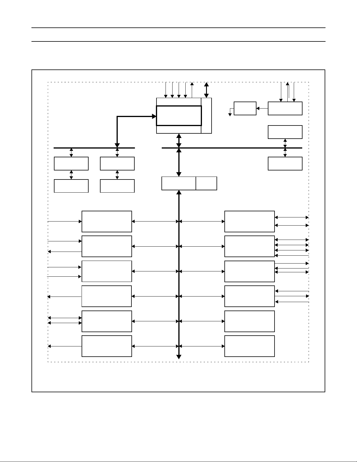
P
hilips Semiconductors Preliminary User Manu
al
LPC2131/2132/2138ARM-based Microcontroller
BLOCK DIAGRAM
ARM7 Local Bus
Internal SRAM
Controller
8/16/32 kB
SRAM
EINT3:0
8 x CAP0
8 x MAT
AD0.7:0
2
AD1.7:0
3
A
out
Internal Flash
Controller
32/64/512 kB
FLASH
External
Interrupts
Capture / Compare
(w/ external clock)
TIMER 0 & 1
A/D Converters
0 and 1
D/A Converter
2
2
1
1
TMS
TRST
Test/Debug Interface
1
1
1
TDI
TCK
TDO
ARM7TDMI-S
AHB Bridge
AHB to VPB
Bridge
VPB (VLSI
Peripheral Bus)
PLL
System
Module
Emulation Trace
(Advanced High-performance Bus)
Clock
AMBA AHB
VPB
Divider
I2C Serial
Interfaces 0 and 1
SPI and SSP
Serial Interfaces
UART 0 & 1
Real Time
Clock
Xtal2
Xtal1
RESET
System
Functions
Vectored Interrupt
Controller
AHB
Decoder
SCL0,1
SDA0,1
SCK0,1
MOSI0,1
MISO0,1
SSEL0,1
TxD0,1
RxD0,1
DSR12,CTS12,RTS1
DTR12, DCD12,RI1
RTXC1
RTXC2
V
bat
2
2
P0.31:0
P1.31:16, 1:0
PWM6:1
1
Shared with GPIO.
2
LPC2138 only.
3
LPC2132/2138 only.
2
General
Purpose I/O
PWM0
Watchdog
Timer
System
Control
Figure 1: LPC2131/2132/2138 Block Diagram
Introduction 19 November 22, 2004
Page 20

P
hilips Semiconductors Preliminary User Manu
al
LPC2131/2132/2138ARM-based Microcontroller
Introduction 20 November 22, 2004
Page 21

P
hilips Semiconductors Preliminary User Manu
al
LPC2131/2132/2138ARM-based Microcontroller
2. LPC2131/2132/2138 MEMORY ADDRESSING
MEMORY MAPS
The LPC2131/2132 /2138 incorporates several distinct memory r egions, shown in t he following figures. Figure 2 shows the overall
map of the entire addr ess sp ace fro m the user p rogra m view point fo llow ing reset. Th e interr upt vec tor area s upport s address remapping, which is described later in this section.
4.0 GB
3.75 GB
3.5 GB
3.0 GB
2.0 GB
1.0 GB
AHB Peripherals
VPB Peripherals
Reserved Address
Space
Boot Block
(re-mapped from On-Chip Flash memory)
Reserved Address Space
32 kB On-Chip Static RAM (LPC2138)
16 kB On-Chip Static RAM (LPC2132)
8 kB On-Chip Static RAM (LPC2131)
0xFFFF FFFF
0xF000 0000
0xE000 0000
0xC000 0000
0x8000 0000
0x4000 8000
0x4000 7FFF
0x4000 4000
0x4000 3FFF
0x4000 2000
0x4000 1FFF
0x4000 0000
Reserved Address Space
0x0008 0000
512 kB On-Chip No n-Volatile Memo ry (LPC2138)
64 kB On-Chip Non-Volatile Memory (LPC21 32)
32 kB On-Chip Non-Volatile Memory (LPC2131)
0.0 GB
Figure 2: System Memory Map
LPC2131/2132/2138 Memory Addressing 21 November 22, 2004
0x0007 FFFF
0x0001 0000
0x0000 FFFF
0x0000 8000
0x0000 7FFF
0x0000 0000
Page 22

P
hilips Semiconductors Preliminary User Manu
al
LPC2131/2132/2138ARM-based Microcontroller
Notes:
- AHB section is
128 x 16 kB blocks
(totaling 2 MB).
- VPB section is
128 x 16 kB blocks
(totaling 2 MB).
4.0 GB
4.0 GB - 2 MB
3.75 GB
AHB Peripherals
0xFFFF FFFF
0xFFE0 0000
0xFFDF FFFF
Reserved
0xF000 0000
0xEFFF FFFF
Reserved
3.5 GB + 2 MB
0xE020 0000
0xE01F FFFF
VPB Peripherals
3.5 GB
0xE000 0000
Figure 3: Peripheral Memory Map
Figures 3 through 5 show different views of the peripheral address space. Both the AHB and VPB peripheral areas are 2
megabyte spaces whic h are divided up into 128 periph erals. Each peripheral space is 16 kilobytes in size . This allows simplifyi ng
the address decod ing for ea ch perip heral. All periphera l registe r addresses are wor d aligned (to 32-bit b oundar ies) regard less of
their size. This eliminate s th e nee d for byte lane mapping hardwa re tha t w oul d be requi red to all ow by te (8-bit) or half-word (16bit) accesses to occur at smaller boundaries. An implication of this is that word and half-word registers must be accessed all at
once. For example, it is not possible to read or write the upper byte of a word register separately.
LPC2131/2132/2138 Memory Addressing 22 November 22, 2004
Page 23
P
hilips Semiconductors Preliminary User Manu
al
LPC2131/2132/2138ARM-based Microcontroller
Vectored Interrupt Controller
(AHB peripheral #126)
(AHB peripheral #125)
(AHB peripheral #124)
(AHB peripheral #3)
(AHB peripheral #2)
0xFFFF F000 (4G - 4K)
0xFFFF C000
0xFFFF 8000
0xFFFF 4000
0xFFFF 0000
0xFFE1 000 0
0xFFE0 C000
(AHB peripheral #1)
(AHB peripheral #0)
Figure 4: AHB Peripheral Map
0xFFE0 800 0
0xFFE0 400 0
0xFFE0 000 0
LPC2131/2132/2138 Memory Addressing 23 November 22, 2004
Page 24
P
hilips Semiconductors Preliminary User Manu
al
LPC2131/2132/2138ARM-based Microcontroller
System Control Block
(VPB peripheral #127)
(VPB peripherals #28- 126)
not used
DAC
(VPB peripheral #27)
SSP
(VPB peripheral #26)
not used
(VPB peripheral #25)
10 bit AD1 (LPC2138)
(VPB peripheral #24)
2
I
C1
(VPB peripheral #23)
not used
(VPB peripheral #14-22)
10 bit AD0
(VPB peripheral #13)
not used
(VPB peripheral #12)
Pin Connect Block
(VPB peripheral #11)
GPIO
(VPB peripheral #10)
RTC
(VPB peripheral #9)
SPI0
(VPB peripheral #8)
2
C0
I
(VPB peripheral #7)
not used
(VPB peripheral #6)
PWM
(VPB peripheral #5)
UART1
(VPB peripheral #4)
UART0
(VPB peripheral #3)
TIMER1
(VPB peripheral #2)
TIMER0
(VPB peripheral #1)
Watchdog Timer
(VPB peripheral #0)
0xE01F FFFF
0xE01F C000
0xE007 0000
0xE006 C000
0xE006 8000
0xE006 4000
0xE006 0000
0xE005 C000
0xE003 8000
0xE003 4000
0xE003 0000
0xE002 C000
0xE002 8000
0xE002 4000
0xE002 0000
0xE001 C000
0xE001 8000
0xE001 4000
0xE001 0000
0xE000 C000
0xE000 8000
0xE000 4000
0xE000 0000
Figure 5: VPB Peripheral Map
LPC2131/2132/2138 Memory Addressing 24 November 22, 2004
Page 25

P
hilips Semiconductors Preliminary User Manu
al
LPC2131/2132/2138ARM-based Microcontroller
LPC2131/2132/2138 MEMORY RE-MAPPING AND BOOT BLOCK
Memory Map Concepts and Operating Modes
The basic concept on the LPC21 31/2132/2138 is that each mem ory area has a " natural " location i n the memo ry map. Thi s is the
address range for which code residing in that area is written. The bulk of each memory space remains permanently fixed in the
same location, eliminating the need to have portions of the code designed to run in different address ranges.
Because of the location of the interrupt vectors on the ARM7 processor (at addresses 0x0000 0000 through 0x0000 001C, as
shown in Table 2 below), a sma ll portion of the Boot Blo ck and SRAM spa ces need to be re-ma pped in order to al low alternati ve
uses of interrupts in the different operating modes described in Table 3. Re-mapping of the interrupts is accomplished via the
Memory Mapping Control feature described in the System Control Block section.
Table 2: ARM Exception Vector Locations
Address Exception
0x0000 0000 Reset
0x0000 0004 Undefined Instruction
0x0000 0008 Software Interrupt
0x0000 000C Prefetch Abort (instruction fetch memory fault)
0x0000 0010 Data Abort (data access memory fault)
0x0000 0014 Reserved *
0x0000 0018 IRQ
0x0000 001C FIQ
*: Identified as reserved in ARM do cumen tation , this loca tion is us ed by the Boot Loader as the Valid User Progra m key. Thi s is
descibed in detail in Flash Memory System and Programming on page 225.
Table 3: LPC2131/2132/2138 Memory Mapping Modes
Mode Activation Usage
Boot Loader
mode
User Flash
mode
User RAM
mode
Hardware activation
by any Reset
Software activation
by Boot code
Software activation
by User program
The Boot Loader always
mapped to the bottom of memory to allow handling exceptions and using interrupts
during the Boot Loading process.
Activated by Boot Loader whe n a valid User Program Si gnature is recogni zed in memory
and Boot Loader operation is not forced. Interrupt vectors are not re-mapped and are
found in the bottom of the Flash memory.
Activated by a User Program as de sir ed. In terru pt ve ctors are re-mapped to the bottom
of the Static RAM.
executes after any reset. The Boot Block interrupt vectors are
LPC2131/2132/2138 Memory Addressing 25 November 22, 2004
Page 26

P
hilips Semiconductors Preliminary User Manu
al
LPC2131/2132/2138ARM-based Microcontroller
Memory Re-Mapping
In order to allo w for com patibili ty with future der ivatives , the en tire Boot Block i s mapped to the top of t he on -chip mem ory space.
In this manner, the use of larger or smaller flash modules will not require changing the location of the Boot Block (which would
require changing the Boot Loader code itself ) or changing the mappin g of the Boot Block interru pt vectors. Memo ry spaces other
than the interrupt vectors remain in fixed locations. Figure 6 shows the on-chip memory mapping in the modes defined above.
The portion of memory that is re-mapped to allow interrupt processing in different modes includes the interrupt vector area (32
bytes) and an additional 32 bytes, for a total of 64 bytes. The re-mapped code locations ove rlay addresses 0x0000 0000 throu gh
0x0000 003F. A typical u ser progra m in th e Flash memory c an place the entir e FIQ h andler at addre ss 0x0000 001C w ithout a ny
need to consider memory boundaries. The vector contained in the SRAM, external memory, and Boot Block must contain
branches to the actual interrupt handlers, or to other instructions that accomplish the branch to the interrupt handlers.
There are three reasons this configuration was chosen:
1. To give the FIQ handler in the Flash memory the advantage of not having to take a memory boundary caused by the remapping into account.
2. Minimize the need to for th e SRAM and Bo ot Blo ck vec to rs to deal with arbitrary boun dari es in th e mi ddl e of cod e sp ac e.
3. To provide space to store constants for jumping beyond the range of single word branch instructions.
Re-mapped memory are as, includin g the Boot Block and interr upt vectors, con tinue to appear in their original loc ation in additi on
to the re-mapped address.
Details on re-mapping and examples can be found in System Control Block on page 29.
LPC2131/2132/2138 Memory Addressing 26 November 22, 2004
Page 27

P
hilips Semiconductors Preliminary User Manu
al
LPC2131/2132/2138ARM-based Microcontroller
0x8000 0000
2.0 GB
2.0 GB - 8K
12K byte Boot Block
(re-mapped from top of Flash memory)
(Boot Block interrupt vectors)
Reserved Addressing Space
0x7FFF FFFF
1.0 GB
32 kB On-Chip SRAM
(SRAM interrupt vectors)
Reserved Addressing Space
(12k byte Boot Block re-Mapped to higher address range)
512K byte Flash Memory
0x4000 8000
0x4000 7FFF
0x4000 0000
0x3FFF FFFF
0x0008 0000
0x0007 FFFF
0.0 GB
Note: memory regions are not drawn to scale.
Active interrupt vectors (from Flash, SRAM, or Boot Block)
0x0000 0000
Figure 6: Map of lower memory is showing re-mapped and re-mappable areas (LPC2138 with 512 kB Flash).
LPC2131/2132/2138 Memory Addressing 27 November 22, 2004
Page 28

P
hilips Semiconductors Preliminary User Manu
al
LPC2131/2132/2138ARM-based Microcontroller
PREFETCH ABORT AND DATA ABORT EXCEPTIONS
The LPC2131/2132/2138 ge nerates the ap propriate bus cycle abort exce ption if an acc ess is attempte d for an address tha t is in
a reserved or unassigned address region. The regions are:
• Areas of the memory map that are not implemented for a specific ARM derivative. For the LPC2131/2132/2138, this is:
- Address space between On-Chip Non-Volatile Memory and On-Chip SRAM, labelled "Reserved Addressing Space" in
Figure 2 and Figure 6. For 32 kB Flash device this is memory address range from 0x0000 8000 to 0x3FFF FFFF, for 64 kB
Flash device this is memory address range from 0x0001 0000 to 0x3FFF FFFF, while for 512 kB Flash device this range is
from 0x0008 0000 to 0x3FFF FFFF.
- Address space between On-Chi p S ta tic RAM and Ex ternal Me mory. Labell ed "Rese rved Ad dressing Space" in Figure 2. For
8 kB SRAM device this is memory address range from 0x4000 1FFF to 0x7FFF DFFFF, for 16 kB SRAM device this is
memory address range from 0x4000 3FFF to 0x7FFF DFFF, while for 32 kB SRAM device this range is from 0x4000 7FFF
to 0x7FFF D000. This is an address range from 0x4000 3FFF to 0x7FFF D000.
- Reserved regions of the AHB and VPB spaces. See Figure 3.
• Unassigned AHB peripheral spaces. See Figure 4.
• Unassigned VPB peripheral spaces. See Figure 5.
For these areas, both atte mpted data acc ess and instruc tion fetch gen erate an excep tion. In additi on, a Prefetch Abort exceptio n
is generated for any instruction fetch that maps to an AHB or VPB peripheral address.
Within the addres s spa ce of an ex is tin g VPB peri phe ral, a data abort exception is not genera ted in res po ns e to an ac ce ss to an
undefined address. Address decoding within eac h peri phe ral is li mit ed to that ne ede d to di stinguish defined regist ers wi thin the
peripheral itself. Fo r example, an access to address 0xE0 00D000 (an un defined add ress wit hin the UART0 space) may result in
an access to the register defined at address 0xE000C000. Details of such address aliasing within a peripheral space are not
defined in the LPC2131/2132/2138 documentation and are not a supported feature.
Note that the ARM core stores the Prefetch Abort flag along with the associated instruction (which will be meaningless) in the
pipeline and processes the abort only if an attempt is made to execute the instruction fetched from the illegal address. This
prevents acciden tal abort s that co uld be ca used by prefetc hes tha t occur w hen co de is ex ecute d very ne ar a memo ry boun dary.
LPC2131/2132/2138 Memory Addressing 28 November 22, 2004
Page 29

P
hilips Semiconductors Preliminary User Manu
al
LPC2131/2132/2138ARM-based Microcontroller
3. SYSTEM CONTROL BLOCK
SUMMARY OF SYSTEM CONTROL BLOCK FUNCTIONS
The System Control Block includes several system features and control registers for a number of functions that are not related
to specific peripheral devices. These include:
• Crystal Oscillator.
• External Interrupt Inputs.
• Memory Mapping Control.
•PLL.
• Power Control.
•Reset.
• VPB Divider.
• Wakeup Timer.
Each type of fu nction has it s own reg ister(s) if any are required and unnee ded bits a re defined as reserved i n order to allow future
expansion. Unrelated functions n ever share the same register addresses.
PIN DESCRIPTION
Table 4 shows pins that are associated with System Control block functions.
Table 4: Pin summary
Pin name Pin direction Pin Description
X1 Input Crystal Oscillator Input- Input to the oscillator and internal clock generator circuits.
X2 Output Crystal Oscillator Output- Output from the oscillator amplifier.
External Interrupt Input 0- An ac tive low general p urpose interru pt input. This pin may be
EINT0 Input
EINT1 Input
EINT2 Input
used to wake up the processor from Idle or Power down modes.
Pins P0.1 and P0.16 can be selected to perform EINT0 function.
External Interrupt Input 1- See the EINT0 description above.
Pins P0.3 and P0.14 can be selected to perform EINT1 function.
LOW level on pin P0.14 immediately after reset is considered as an external hardware
request to start the ISP c ommand handler. M ore details on I SP and Serial Boot Load er can
be found in "Flash Memory System and Programming" chapter.
External Interrupt Input 2- See the EINT0 description above.
Pins P0.7 and P0.15 can be selected to perform EINT2 function.
External Interrupt Input 3- See the EINT0 description above.
EINT3 Input
Pins P0.9, P0.20 and P0.30 can be selected to perform EINT3 function.
R
ESET Input
System Control Block 29 November 22, 2004
External Reset input- A low on this pin resets the chi p, causing I/O ports and periphe rals
to take on their default states, and the processor to begin execution at address 0.
Page 30
P
hilips Semiconductors Preliminary User Manu
al
LPC2131/2132/2138ARM-based Microcontroller
REGISTER DESCRIPTION
All registers, regardless of size, are on word address boundaries. Details of the registers appear in the description of each
function.
Table 5: Summary of System Control Registers
Name Description Access
External Interrupts
EXTINT External Interrupt Flag Register. R/W 0 0xE01FC140
EXTWAKE External Interrupt Wakeup Register. R/W 0 0xE01FC144
EXTMODE External Interrupt Flag Register. R/W 0 0xE01FC148
EXTPOLAR External Interrupt Wakeup Register. R/W 0 0xE01FC14C
Memory Mapping Control
MEMMAP Memory Mapping Control. R/W 0 0xE01FC040
Phase Locked Loop
PLLCON PLL Control Register. R/W 0 0xE01FC080
PLLCFG PLL Configuration Register. R/W 0 0xE01FC084
PLLSTAT PLL Status Register. RO 0 0xE01FC088
PLLFEED PLL Feed Register. WO NA 0xE01FC08C
Power Control
PCON Power Con trol Register. R/W 0 0xE01FC0C0
PCONP Power Control for Peripherals. R/W 0x3BE 0xE01FC0C4
VPB Divider
VPBDIV VPB Divider Control. R/W 0 0xE01FC100
Reset
Value*
Address
Reset
RSID Reset Source Identification Register R/W 0 0xE01FC180
Code Security/Debugging
CSPR Code Security Protection Register RO 0 0xE01FC184
*Reset Value refers to the data stored in used bits only. It does not include reserved bits content.
System Control Block 30 November 22, 2004
Page 31

P
hilips Semiconductors Preliminary User Manu
al
LPC2131/2132/2138ARM-based Microcontroller
CRYSTAL OSCILLATOR
While an input signal of 50-50 duty cycle within a frequency range from 1 MHz to 50 MHz can be used by LPC2131/2132/2138
if supplied to its input XTAL1 pin, this microcont roller’s onb oard osc illator circui t supports external c rystals in the rang e of 1 MHz
to 30 MHz only . If o n-chip PLL s yste m or boot-lo ader i s us ed, i nput c lock fre quenc y is lim ited t o exc lusive range of 10 MH z to 25
MHz.
The oscillator output freq uen cy is ca lle d F
equations, etc. else where in t his d ocum ent. F
and the ARM processor clock frequenc y is referred to as cclk for purposes of rate
osc
and cclk are the same val ue unless the PLL is running and con nected. Refer to
osc
the PLL description in this chapter for details and frequency limitations.
Onboard oscillator in LPC2131/2132/2138 can operate in one of two modes: slave mode and oscillation mode.
In slave mode the input clock signal should be coupled by means of a capacitor of 100 pF (Cc in Figure 7, drawing a), with an
amplitude of at leas t 200mVrms. X2 pin in this co nfig ura tion can be left not connected. If slave mode is se lec ted , F
signal of
osc
50-50 duty cycle can range from 1 MHz to 50 MHz.
External components and models used in oscillation mode are shown in Figure 7, drawings b and c, and in Table 6. Since the
feedback resistance is integrated on chip, only a crystal and the capacitances C
case of fundamental mode oscillati on (the fun damen tal freque ncy is repres ented by L, C
drawing c, represents the par all el pa ck age cap aci tance and should not be larger than 7 pF. Parameters F
and CX2 need to be connected externally in
X1
and RS). Capacitance Cp in Figure 7,
L
, CL, RS and CP are
C
supplied by the crystal manufa ctu rer.
Choosing an oscillation mode as an on-board oscillator mode of operation limits F
LPC2131/2132/2138
X1 X2
C
C
Clock
LPC2131/2132/2138
X1 X2
C
X1
Xtal
C
X2
clock selection to 1 MHz to 30 MHz.
osc
L
<=>
C
R
C
L
S
P
a) b) c)
Figure 7: Oscillator modes and models: a) slave mode of operation, b) oscillation mode of operation,
c) external crystal model used for C
Table 6: Recommended values for C
Fundamental Oscillation
Frequency F
C
Capacitance C
in oscillation mode (crystal and external components parameters)
X1/X2
Crystal Load
L
Max. Crystal Series
Resistance R
10 pF n.a. n.a.
1 - 5 MHz
20 pF n.a. n.a.
30 pF < 300 : 58 pF, 58 pF
System Control Block 31 November 22, 2004
X1/X2
evaluation
S
External Load
Capacitors C
X1
, C
X2
Page 32

P
hilips Semiconductors Preliminary User Manu
al
LPC2131/2132/2138ARM-based Microcontroller
Table 6: Recommended values for C
Fundamental Oscillation
Frequency F
C
Capacitance C
5 - 10 MHz
10 - 15 MHz
15 - 20 MHz
20 - 25 MHz
25 - 30 MHz
in oscillation mode (crystal and external components parameters)
X1/X2
Crystal Load
L
Max. Crystal Series
Resistance R
S
External Load
Capacitors C
10 pF < 300 : 18 pF, 18 pF
20 pF < 300 : 38 pF, 38 pF
30 pF < 300 : 58 pF, 58 pF
10 pF < 300 : 18 pF, 18 pF
20 pF < 220 : 38 pF, 38 pF
30 pF < 140 : 58 pF, 58 pF
10 pF < 220 : 18 pF, 18 pF
20 pF < 140 : 38 pF, 38 pF
30 pF < 80 : 58 pF, 58 pF
10 pF < 160 : 18 pF, 18 pF
20 pF < 90 : 38 pF, 38 pF
30 pF < 50 : 58 pF, 58 pF
10 pF <130 : 18 pF, 18 pF
20 pF <50 : 38 pF, 38 pF
30 pF n.a. n.a.
X1
, C
X2
f
selection
OSC
on-chip PLL used
in application?
False
ISP used for initial
code download?
False
external crystal
oscillator used?
False
min f
= 1 MHz
OSC
max f
= 50 MHz
OSC
True
min f
max f
= 1 MHz
OSC
= 30 MHz
OSC
min f
max f
= 10 MHz
OSC
= 25 MHz
OSC
True
True
(Figure 7, mode a and/or b) (Figure 7, mode a) (Figure 7, mode b)
Figure 8: F
selection algorithm
OSC
System Control Block 32 November 22, 2004
Page 33

P
hilips Semiconductors Preliminary User Manu
al
LPC2131/2132/2138ARM-based Microcontroller
EXTERNAL INTERRUPT INPUTS
The LPC2131/2132/2138 includes four External Interrupt Inputs as selectable pin functions. The External Interrupt Inputs can
optionally be used to wake up the processor from the Power Down mode.
Register Description
The external interrupt function has four registers associated with it. The EXTINT register contains the interrupt flags, and the
EXTWAKEUP register contains bits that enable individual external interrupts to wake up the LPC2131/2132/2138 from Power
Down mode. The EXTMODE and EXTPOLAR registers specify the level and edge sensitivity parameters.
Table 7: External Interrupt Registers
Address Name Description Access
0xE01FC140 EXTINT
0xE01FC144 EXTWAKE
0xE01FC148 EXTMODE
0xE01FC14C EXTPOLAR
The External Interrupt Flag Register contains interrupt flags for EINT0, EINT1,
and EINT2. See Table 8.
The External Interrupt Wakeup Register contains three enable bits that control
whether each external inte rrup t will ca use the proc es so r to w ake u p fro m Pow e r
Down mode. See Table 9.
The External Interrupt Mode R egister co ntrols whethe r each pin is edge- or levelsensitive.
The External Interrupt Polarity Regi ster controls w hich leve l or edge on ea ch pin
will cause an interrupt.
R/W
R/W
R/W
R/W
External Interrupt Flag Register (EXTINT - 0xE01FC140)
When a pin is selected for its external interrupt function, the level or edge on that pin se le cte d by its bi ts i n the EXTPOLAR and
EXTMODE registers will set its interrupt flag in this register. This asserts the corresponding interrupt request to the VIC, which
will cause an interrupt if interrupts from the pin are enabled.
Writing ones to bits EINT0 thr ough EINT3 in EXTINT register cl ears the corre sponding bits. In level-se nsitive m ode this action is
efficacious only when the pin is in its inactive state.
Once a bit from EINT0 to EINT3 is set a nd an appropri ate code star ts to execute (handling wak eup and/or exter nal interru pt), this
bit in EXTINT register must be cleared. O therwise eve nt that was just triggered by a ctivity on the EINT pin wil l not be recogn ized
in future.
For example, if a sy stem w akes up from power-do wn using l ow level on externa l interrupt 0 pin, its post- wakeup co de must re set
EINT0 bit in order to allow future entry into the power-down mode. If EINT0 bit is left set to 1, subsequent attempt(s) to invoke
power-down mode will fail. The same goes for external interrupt handling.
More details on power-down mode will be discussed in the following chapters.
System Control Block 33 November 22, 2004
Page 34

P
hilips Semiconductors Preliminary User Manu
al
LPC2131/2132/2138ARM-based Microcontroller
Table 8: External Interrupt Flag Register (EXTINT - 0xE01FC140)
EXTINT Function Description
In level-sensitive mode, this bit is set i f the EINT0 func tion is selec ted for its p in, and
the pin is in its active state. In edge-sensitive mode, this bit is set if the EINT0
function is selected for its pin, and the selected edge occurs on the pin.
0EINT0
Up to two pins can be selected to perform EINT0 function (see P0.1 and P0.16
description in "Pin Configuration" chapter.)
This bit is cleared by writi ng a one to it, except in level sensit ive mode when the pi n
is in its active state.
In level-sensitive mode, this bit is set i f the EINT1 func tion is selec ted for its p in, and
the pin is in its active state. In edge-sensitive mode, this bit is set if the EINT1
function is selected for its pin, and the selected edge occurs on the pin.
1EINT1
Up to two pins can be selected to perform EINT1 function (see P0.3 and P0.14
description in "Pin Configuration" chapter.)
This bit is cleared by writi ng a one to it, except in level sensit ive mode when the pi n
is in its active state.
In level-sensitive mode, this bit is set i f the EINT2 func tion is selec ted for its p in, and
the pin is in its active state. In edge-sensitive mode, this bit is set if the EINT2
function is selected for its pin, and the selected edge occurs on the pin.
2EINT2
Up to two pins can be selected to perform EINT2 function (see P0.7 and P0.15
description in "Pin Configuration" chapter.)
Reset
Value
0
0
0
This bit is cleared by writi ng a one to it, except in level sensit ive mode when the pi n
is in its active state.
In level-sensitive mode, this bit is set i f the EINT3 func tion is selec ted for its p in, and
the pin is in its active state. In edge-sensitive mode, this bit is set if the EINT3
function is selected for its pin, and the selected edge occurs on the pin.
3EINT3
Up to three pins can be selected to perform EINT3 function (see P0.9, P0.20 and
0
P0.30 description in "Pin Configuration" chapter.)
This bit is cleared by writi ng a one to it, except in level sensit ive mode when the pi n
is in its active state.
7:4 Reserved
Reserved, user software should not write ones to reserved bits. The value read
from a reserved bit is not defined.
NA
Interrupt Wakeup Register (INTWAKE - 0xE01FC144)
Enable bits in the EXTWAKE register allow the external interrupts to wake up the processor if it is in Power Down mode. The
related EINTn function must be mapped to the pin in order for the wakeup process to take place. It is not necessary for the
interrupt to be enabled in the Vectored Interrupt Controller for a wakeup to take place. This arrangement allows additional
capabilities, such as having an external interrupt input wake up the processor from Power Down mode without causing an
interrupt (simply resuming operation), or allowing an interrupt to be enabled during Power Down without waking the processor
up if it is asserted (eliminating the need to disable the interrupt if the wakeup feature is not desirable in the application).
System Control Block 34 November 22, 2004
Page 35

P
hilips Semiconductors Preliminary User Manu
al
LPC2131/2132/2138ARM-based Microcontroller
Table 9: Interrupt Wakeup Register (INTWAKE - 0xE01FC144)
EXTWAKE Function Description
0 EXTWAKE0 When one, assertion of EINT0
1 EXTWAKE1 When one, assertion of EINT1
2 EXTWAKE2 When one, assertion of EINT2
3 EXTWAKE3 When one, assertion of EINT3 will wake up the processor from Power Down mode. 0
13:4 Reserved
14 BODWAKE When one, BOD interrupt will wake up the processor from Power Down mode.
15 RTCWAKE
Reserved, user software should not write ones to reserved bits. The value read
from a reserved bit is not defined.
When one, assertion of an RT C interrupt will wake the processor from Power Down
mode.
will wake up the processor from Power Down mode. 0
will wake up the processor from Power Down mode. 0
will wake up the processor from Power Down mode. 0
Reset
Value
0
External Interrupt Mode Register (EXTMODE - 0xE01FC148)
The bits in thi s registe r select whether ea ch EINT pin is level- o r edge-se nsitive. Only pin s that are select ed for the EINT fu nction
(chapter Pin Connect Blo ck on p age 81) a nd e nabled via the VICIntEnable register (chapter Vectored Inte rrupt Controller (VIC)
on page 61) can cause interrupts from the External Interrupt function (though of course pins selected for) other functions may
cause interrupts from those funct ion s).
Note: Software should only change a bit in this regis ter when its interrupt is disable d in VICIntEnable, and sh ould write
the corresponding 1 to EXTINT before re-enabling the interrupt, to clear the EXTINT bit that could be set by changing
the mode.
Table 10: External Interrupt Mode Register (EXTMODE - 0xE01FC148)
EXTMODE Function Description
0 EXTMODE0 When 0, level-sensitivity is selected for EINT0. When 1, EINT0 is edge-sensitive. 0
1 EXTMODE1 When 0, level-sensitivity is selected for EINT1. When 1, EINT1 is edge-sensitive. 0
2 EXTMODE2 When 0, level-sensitivity is selected for EINT2. When 1, EINT2 is edge-sensitive. 0
3 EXTMODE3 When 0, level-sensitivity is selected for EINT3. When 1, EINT3 is edge-sensitive. 0
7:4 Reserved
Reserved, user software should not write ones to reserved bits. The value read
from a reserved bit is not defined.
Reset
Value
NA
External Interrupt Polarity Register (EXTPOLAR - 0xE01FC14C)
In level-sensitive mode, the bits in this register select whether the corresponding pin is high- or low-active. In edge-sensitive
mode, they select whether the pin is rising- or falling-edge sensitive. Only pins that are selected for the EINT function (chapter
Pin Connect Block on page 81) and enabled in the VICIntEnable register (chapter Vectored Interrupt Controller (VIC) on page
61) can cause interrupts from the External Interrupt function (though of course pins selected for other functions may cause
interrupts from those functions ).
Note: Software should only change a bit in this regis ter when its interrupt is disable d in VICIntEnable, and sh ould write
the corresponding 1 to EXTINT before re-enabling the interrupt, to clear the EXTINT bit that could be set by changing
the polarity.
System Control Block 35 November 22, 2004
Page 36

P
hilips Semiconductors Preliminary User Manu
al
LPC2131/2132/2138ARM-based Microcontroller
Table 11: External Interrupt Polarity Re gister (EXTPOLAR - 0xE01FC14C)
EXTPOLAR Function Description
0 EXTPOLAR0
1 EXTPOLAR1
2 EXTPOLAR2
3 EXTPOLAR3
7:4 Reserved
When 0, EINT0 is low-active or falling-edge sensitive (depending on EXTMODE0).
When 1, EINT0 is high-active or rising-edge sensitive (depending on EXTMODE0).
When 0, EINT1 is low-active or falling-edge sensitive (depending on EXTMODE1).
When 1, EINT1 is high-active or rising-edge sensitive (depending on EXTMODE1).
When 0, EINT2 is low-active or falling-edge sensitive (depending on EXTMODE2).
When 1, EINT2 is high-active or rising-edge sensitive (depending on EXTMODE2).
When 0, EINT3 is low-active or falling-edge sensitive (depending on EXTMODE3).
When 1, EINT3 is high-active or rising-edge sensitive (depending on EXTMODE3).
Reserved, user softw are should n ot write o nes to reser ved bits . The valu e read from
a reserved bit is not defined.
Reset
Value
0
0
0
0
NA
Multiple External Interrupt Pins
Software can select multiple pins for each of EINT3:0 in the Pin Select registers, which are described in chapter Pin Connect
Block on page 81. The external interrupt logic for each of EINT3:0 receives the state of all of its associated pins from the pins’
receivers, alon g with signals th at indic ate wh ether each p in is selected for the EINT functi on. The e xternal interrupt l ogic ha ndles
the case when more than one pin is so selected, differently according to the state of its Mode and Polarity bits:
• In Low-Active Le vel Sensitiv e mode, the stat es of all p ins select ed for EINT functi onality ar e digitally co mbined usin g a positive
logic AND gate.
• In High-Active Le vel Sensitive mode , the states of all p ins selected fo r EINT functionali ty are digitally c ombined using a po sitive
logic OR gate.
• In Edge Sensitive mode, regardless of polarity, the pin with the lowest GPIO port number is used. (Selecting multiple EINT pins
in edge-sensitive mode could be considered a programming error.)
The signal derived by this logic is the EINTi signal in the following logic schematic (Figure 9).
When more than one EINT pi n is logically ORed , the interrupt service ro utine can read the s tates of the pins from G PIO port using
IO0PIN and IO1PIN registers, to determine which pin(s) caused the interrupt.
System Control Block 36 November 22, 2004
Page 37

P
hilips Semiconductors Preliminary User Manu
al
LPC2131/2132/2138ARM-based Microcontroller
EINTi
EXTPOLARi
EXTMODEi
Write 1 to EXTINTi
VPB Bus Data
Glitch
Filter
Reset
Wakeup Enable
(one bit of EXTWAKE)
QD
pclk
1
S
D
Q
R
Figure 9: External Interrupt Logic
VPB Read
of EXTWAKE
EINTi to
Wakeup Timer
(Figure 11)
Interrupt Flag
(one bit of EXTINT)
S
Q
R
pclk pclk
S
Q
R
to VIC
VPB Read
of EXTINT
System Control Block 37 November 22, 2004
Page 38

P
hilips Semiconductors Preliminary User Manu
al
LPC2131/2132/2138ARM-based Microcontroller
MEMORY MAPPING CONTROL
The Memory Mapping Control alters the mapping of the interrupt vectors that appear beginning at address 0x00000000. This
allows code running in different memory spaces to have control of the interrupts.
Memory Mapping Control Register (MEMMAP - 0xE01FC040)
()
Table 12: MEMMAP Register
Address Name Description Access
0xE01FC040 MEMMAP
Memory mapping control. Selects whether the ARM interrupt vectors are read
from the Flash Boot Block, User Flash, or RAM.
R/W
Table 13: Memory Mapping Control Register (MEMMAP - 0xE01FC040)
MEMMAP Function Description
Reset
Value*
00: Boot Loader Mode. Interrupt vectors are re-mapped to Boot Block.
01: User Flash Mode. Interrupt vectors are not re-mapped and reside in Flash.
1:0 MAP1:0
10: User RAM Mode. Interrupt vectors are re-mapped to Static RAM.
11: Reserved. Do not use this option.
0
Warning: Improper set tin g of t his v alue may result in inco rrect o perati on of the devi ce.
7:2 Reserved
Reserved, user software shou ld not write ones to reserved b its. The value rea d from a
reserved bit is not defined.
NA
*: The hardware reset value of the MAP bits is 00 for LPC2131/2132/2138 parts. The appare nt reset va lue that the user will see
will be altered by the Boot Loader code, which always runs initially at reset. User documentation will reflect this difference.
Memory Mapping Control Usage Notes
Memory Mapping Cont rol simply selects one out of three available sources of data (sets of 64 bytes each) nec essary for handling
ARM exceptions (interrupts).
For example, whenever a Software Interrupt request is generated, ARM core will always fetch 32-bit data "residing" on 0x0000
0008 (see Table 2, “ARM Exception Vector Locat ions,” on page 25). This mea ns that when MEMMAP[1:0]= 10 (User RAM Mode),
read/fetch from 0x0000 0008 will provide data stored in 0x4000 0008. In case of MEMMAP[1:0]=00 (Boot Loader Mode), read/
fetch from 0x0000 0008 will provide data available also at 0x7FFF E008 (Boot Block remapped from on-chip ROM).
MEMMAP[1:1]=11 (User External Memory Mode) will result in fetching data from off-chip memory at location 0x8000 0008.
System Control Block 38 November 22, 2004
Page 39

P
hilips Semiconductors Preliminary User Manu
al
LPC2131/2132/2138ARM-based Microcontroller
PLL (PHASE LOCKED LOOP)
The PLL accepts an input clock frequency in the range of 10 MHz to 25 MHz only. The input frequency is multiplied up into the
cclk with the range of 10 MHz to 60 MHz using a Current Controlled O scillator (CCO ). The multipli er can be an integ er value from
1 to 32 (in practice, the multiplier value cannot be higher than 6 on the LPC2131/2132/2138 due to the upper frequency limit of
the CPU). The CCO operate s in the ran ge of 156 MHz to 320 MHz, s o there is an addit ional di vider in the loop to ke ep the CC O
within its frequenc y ra nge w hi le t he PL L i s p rov idi ng the desired output frequency. The output d ivi de r ma y be set to divide by 2,
4, 8, or 16 to produce the output clo ck . Sinc e the min im um outp ut divider value is 2, it is insured that the PLL output has a 50%
duty cycle. A block diagram of the PLL is shown in Figure 10.
PLL activation is con trolled via the PLLC ON register. The PLL mu ltiplier and divider v alues are controlle d by the PLLCFG regist er.
These two registers are protected in order to prevent accidental alteration of PLL parameters or deactivation of the PLL. Since
all chip operations, including the Watchdog Timer, are dependent on the PLL when it is providing the chip clock, accidental
changes to the PLL setup could result in unexpected behavior of the microcontroller. The protection is accomplished by a feed
sequence similar to that of the Watchdog Timer. Details are provided in the description of the PLLFEED register.
The PLL is turned off and bypassed fol lowing a chip Reset and when by entering pow er Down mode. PLL is enabled by software
only. The program must configure and activate the PLL, wait for the PLL to Lock, then connect to the PLL as a clock source.
Register Description
The PLL is controlled by the registers shown in Table 14. More detailed descriptions follow.
Warning: Improper setting of PLL values may result in incorrect operation of the device.
Table 14: PLL Registers
Address Name Description Access
PLL Control Register. Holding register for updating PLL control bits. Values
0xE01FC080 PLLCON
0xE01FC084 PLLCFG
0xE01FC088 PLLSTAT
0xE01FC08C PLLFEED
written to this register do not take effect until a valid PLL feed sequ ence has taken
place.
PLL Configuration Register. Holding register for updating PLL configuration
values. Values written to this register do not take effect until a valid PLL feed
sequence has taken place.
PLL Status Register. Read-back register for PLL control and configuration
information. If PLLCON or PLLCFG have been written to, but a PLL feed
sequence has not yet occurred, they will not reflect the current PLL state.
Reading this registe r provides the actual val ues controlling the PL L, as well as the
status of the PLL.
PLL Feed Register. This register enables loading of the PLL control and
configuration information from the PLLCON and PLLCFG registers into the
shadow registers that actually affect PLL operation.
R/W
R/W
RO
WO
System Control Block 39 November 22, 2004
Page 40

P
hilips Semiconductors Preliminary User Manu
al
LPC2131/2132/2138ARM-based Microcontroller
PLLC
PLLE
F
OSC
PSEL[1:0]
PLOCK
MSEL[4:0]
0
0
Direct
pd
Bypass
Phase-
Frequency
Detector
fout
CCO
cd
Div-by-M
msel<4:0>
Clock
Synchronization
pd
F
CCO
pd
1
0
cd
/2P
0
1
0
cclk
1
Figure 10: PLL Block Diagram
PLL Control Register (PLLCON - 0xE01FC080)
The PLLCON register contains the bits that enable and connect the PLL. Enabling the PLL allows it to attempt to lock to the
current settings of th e m ul tipl ie r and di vi der va lues. Connecting the PLL ca us es the pro ce ss or a nd a ll ch ip func ti ons to run fr om
the PLL output clock. Changes to the PLLCO N register d o not take effect until a co rrect PLL fee d sequen ce has been given (se e
PLL Feed Register (PLLFEED - 0xE01FC08C) description).
System Control Block 40 November 22, 2004
Page 41

P
hilips Semiconductors Preliminary User Manu
al
LPC2131/2132/2138ARM-based Microcontroller
Table 15: PLL Control Register (PLLCON - 0xE01FC080)
PLLCON Function Description
0 PLLE
1 PLLC
7:2 Reserved
The PLL must be set up, enabled, and Lock established before it may be used as a clock source. When switching from the
oscillator clock to the PLL output or vice versa, internal circuitry synchronizes the operation in order to ensure that glitches are
not generated. Hardw are does not insu re that the PLL is lo cked bef ore it is con nected or autom atically di sconnec t the PLL i f lock
is lost during opera tion. In the event of l oss of PLL lock, it i s likely that the o scillator clock has become unst able and disconnecting
the PLL will not remedy the situation.
PLL Enable. When one, and after a valid PLL feed, this bit will activate the PLL and
allow it to lock to the requested frequency. See PLLSTAT register, Table 17.
PLL Connect. When PLLC and PLLE are both set to one, and after a valid PLL feed,
connects the PLL as the clock source for the LPLPC2131/2132/2138. Otherwise, the
oscillator clock is u sed directly by the LPLPC21 31/2132/21 38. See PLLSTAT register,
Table 17.
Reserved, user software shou ld not write ones to reserved b its. The value rea d from a
reserved bit is not defined.
Reset
Value
0
0
NA
PLL Configuration Register (PLLCFG - 0xE01FC084)
The PLLCFG register contains the PLL multiplier and divider values. Changes to the PLLCFG register do not take effect until a
correct PLL feed sequenc e has been giv en (see PLL Feed Re gister (PLLFEED - 0xE01FC08C) desc ription). Calcul ations for the
PLL frequency, and multiplier and divider values are found in the PLL Frequency Calculation section.
Table 16: PLL Configuration Register (PLLCFG - 0xE01FC084)
PLLCFG Function Description
PLL Multiplier value. Supplies the value "M" in the PLL frequency calculations.
4:0 MSEL4:0
6:5 PSEL1:0
7 Reserved
Note: For details on sele cting the rig ht value for MSEL 4:0 see sec tion "PLL Frequ ency
Calculation" on page 43.
PLL Divider value. Supplies the value "P" in the PLL frequency calculations.
Note: For details on selecting the right val ue for PSEL1:0 see section "PL L Frequency
Calculation" on page 43.
Reserved, user software shou ld not write ones to reserved b its. The value rea d from a
reserved bit is not defined.
Reset
Value
0
0
NA
PLL Status Register (PLLSTAT - 0xE01FC088)
The read-only PLLSTAT register provides the actual PLL parameters that are in effect at the time it is read, as well as the PLL
status. PLLSTAT may di sagree with values foun d in PLLCON and PLLCFG beca use changes to those re gisters do not take effe ct
until a proper PLL feed has occurred (see PLL Feed Register (PLLFEED - 0xE01FC08C) description).
System Control Block 41 November 22, 2004
Page 42

P
hilips Semiconductors Preliminary User Manu
al
LPC2131/2132/2138ARM-based Microcontroller
Table 17: PLL Status Register (PLLSTAT - 0xE01FC088)
PLLSTAT Function Description
4:0 MSEL4:0 Read-back for the PLL Multiplier value. This is the value currently used by the PLL. 0
6:5 PSEL1:0 Read-back for the PLL Divider value. This is the value currently used by the PLL. 0
7 Reserved
8 PLLE
9 PLLC
10 PLOCK
15:11 Reserved
PLL Interrupt
The PLOCK bit in the PLLSTAT register is connected to the interrupt controller. This allows for software to turn on the PLL and
continue with other fun ctions without having to wait for the PLL to ach ieve lock. Wh en the interru pt occurs (PLOCK = 1), the PLL
may be connected, and the interrupt disabled.
Reserved, user software shou ld not write ones to reserved bits. The value rea d from
a reserved bit is not defined.
Read-back for the PLL Enable bit. When one, the PLL is currently activated. When
zero, the PLL is turne d off. This bit is aut omatically cleared w hen Power Do wn mode
is activated.
Read-back for the PLL Conne ct bit. W hen PLLC and PLLE are both one, the PLL is
connected as the clo ck source for th e LPLPC213 1/2132/21 38. When eith er PLLC or
PLLE is zero, the PLL is bypassed and the oscillator clock is used directly by the
LPC2131/2132/2138. This bit is automatically cleared when Power Down mode is
activated.
Reflects the PLL Lock status . When zero , the PLL is no t locked. Wh en one, the PLL
is locked onto the requested frequency.
Reserved, user software shou ld not write ones to reserved bits. The value rea d from
a reserved bit is not defined.
Reset
Value
NA
0
0
0
NA
PLL Modes
The combinations of PLLE and PLLC are shown in Table 18.
Table 18: PLL Control Bit Combinations
PLLC PLLE PLL Function
0 0 PLL is turned off and disconnected. The system runs from the unmodified clock input.
0 1 The PLL is active, but not yet connected. The PLL can be connected after PLOCK is asserted.
10
1 1 The PLL is active and has been connected as the system clock source.
Same as 0 0 combination. This preven ts the possibility of the PLL bei ng connected without als o being
enabled.
PLL Feed Register (PLLFEED - 0xE01FC08C)
A correct feed sequence mus t be written to the PLLFEED regi ster in or der for chang es to the PLLCO N and PLLCFG reg isters to
take effect. The feed sequence is:
1. Write the value 0xAA to PLLFEED
2. Write the value 0x55 to PLLFEED.
System Control Block 42 November 22, 2004
Page 43

P
hilips Semiconductors Preliminary User Manu
al
LPC2131/2132/2138ARM-based Microcontroller
The two writes must be in the correct sequence, and must be consecutive VPB bus cycles. The latter requirement implies that
interrupts must be disabled for the duration of the PLL feed operation. If either of the feed values is incorrect, or one of the
previously mentioned conditions is not met, any changes to the PLLCON or PLLCFG register will not become effective.
Table 19: PLL Feed Register (PLLFEED - 0xE01FC08C)
PLLFEED Function Description
7:0 PLLFEED
The PLL feed sequence must be written to this register in order for PLL
configuration and control register changes to take effect.
Reset
Value
undefined
PLL and Power Down Mode
Power Down mode automatically turns off and disconnects the PLL. Wakeup from Power Down mode does not automatically
restore the PLL settings, this must be done in software. Typically, a routine to activate the PLL, wait for lock, and then connect
the PLL can be called at the begin ning of a ny inte rrupt service ro utine th at migh t be cal led due to the wake up. It is import ant not
to attempt to restart the PLL by simply feeding it when execution resumes after a wakeup from Power Down mode. This would
enable and connect the PLL at the same time, before PLL lock is established.
PLL Frequency Calculation
The PLL equations use the following parameters:
F
OSC
F
CCO
cclk the PLL output frequency (also the processor clock frequency)
M PLL Multiplier value from the MSEL bits in the PLLCFG register
P PLL Divider value from the PSEL bits in the PLLCFG register
the frequency from the crystal oscillator
the frequency of the PLL current controlled oscillator
The PLL output frequency (when the PLL is both active and connected) is given by:
F
cclk = M * F
or cclk = ———
osc
cco
2 * P
The CCO frequency can be computed as:
F
= cclk * 2 * P or F
cco
cco
= F
* M * 2 * P
osc
The PLL inputs and settings must meet the following:
•F
is in the range of 10 MHz to 25 MHz.
osc
• cclk is in the range of 10 MHz to F
is in the range of 156 MHz to 320 MHz.
•F
cco
System Control Block 43 November 22, 2004
(the maximum allowed frequency for the LPLPC2131/2132/2138).
max
Page 44

P
hilips Semiconductors Preliminary User Manu
al
LPC2131/2132/2138ARM-based Microcontroller
Procedure for Determining PLL Settings
If a particular application uses the PLL, its configuration may be determined as follows:
1. Choose the desired processor operating frequency (cclk). This may be based on processor throughput requirements,
need to support a spec ific set o f UART baud rates, etc. Be ar in m ind that pe riph eral d evices may be run nin g from a lowe r
clock than the processor (see the VPB Divider description in this chapter).
2. Choose an oscillator frequency (F
3. Calculate the value of M to c onfigure the MSEL bits. M = cclk / F
to the MSEL bits in PLLCFG is M - 1 (see Table 21).
4. Find a value for P to con fig ure the PSEL b its, s uc h t hat F
the equation given a bove. P must hav e one of the v alues 1, 2, 4 , or 8. The value writt en to the PSEL bits in PLLCFG is 00
). cclk must be the whole (non-fractional) multiple of F
osc
. M must be in the rang e of 1 to 32 . Th e va lue w ritte n
osc
is within its defined frequency lim its. F
cco
for P = 1; 01 for P = 2; 10 for P = 4; 11 for P = 8 (see Table 20).
Table 20: PLL Divider Values
osc
.
is calculated using
cco
PSEL Bits
(PLLCFG bits 6:5)
00 1
01 2
10 4
11 8
Table 21: PLL Multiplier Values
MSEL Bits
(PLLCFG bits 4:0)
00000 1
00001 2
00010 3
00011 4
... ...
11110 31
11111 32
Value of P
Value of M
PLL Example
System design asks for F
Based on th ese specifications, M = cclk / F
Value for P can be derived from P = F
the lowest allowed fre quency for F
= 10 MHz and requires cclk = 60 MHz.
osc
= 60 MHz / 10 MHz = 6. Consequently, M-1 = 5 will be written as PLLCFG 4:0.
osc
/ (cclk * 2), using condition that F
cco
= 156 MHz, P = 156 MHz / (2*60 MHz) = 1.3. The highest F
cco
must be in range of 156 MHz to 320 M Hz. Assuming
cco
frequency criteria prod uces
cco
P = 2.67. The only solut ion for P tha t sa tis fies both of these requirements and is listed in Table 20 i s P = 2. Th ere f ore , PLLCFG
6:5 = 1 will be used.
System Control Block 44 November 22, 2004
Page 45

P
hilips Semiconductors Preliminary User Manu
al
LPC2131/2132/2138ARM-based Microcontroller
POWER CONTROL
The LPLPC2131/2132/213 8 suppo rts two reduced power modes : Idle mo de and Power D own mode . In Idle mod e, executi on of
instructions is suspended until either a Reset or interrupt occurs. Peripheral functions continue operation during Idle mode and
may generate interrupts to cause the processor to resume execution. Idle mode eliminates power used by the processor itself,
memory systems and related controllers, and internal buses.
In Power Down mode, the oscillator is shut down and the chip receives no internal clocks. The processor state and registers,
peripheral registers, and internal SRAM values are preserved throughout Power Down mode and the logic levels of chip pins
remain static. The Power Down mode can be terminated and normal operation resumed by either a Reset or certain specific
interrupts that are able to function without clocks. Since all dynamic operation of the chip is suspended, Power Down mode
reduces chip power consumption to nearly zero.
Entry to Power Down and Idle mode s must be coord inated with program ex ecution. Wake up from Power Down or Id le modes via
an interrupt resumes program execut ion in such a wa y that no instru ctions are los t, incomplete, or repeated. Wake u p from Power
Down mode is discussed further in the description of the Wakeup Timer later in this chapter.
A Power Control for Peripherals feature allows individual peripherals to be turned off if they are not needed in the application,
resulting in additional power savings.
Register Description
The Power Control function contains two registers, as shown in Tabl e 22. More detailed descriptions follow.
Table 22: Power Control Registers
Address Name Description Access
0xE01FC0C0 PCON
0xE01FC0C4 PCONP
Power Control Register. This register contains control bits that enable the two
reduced power operating modes of the LPLPC2131/2132/2138. See Table 23.
Power Control for Peripheral s Register. This register contains control bits that
enable and disable indiv idual pe riphera l functi ons, Allo wing elim inati on of pow er
consumption by peripherals that are not needed.
R/W
R/W
Power Control Register (PCON - 0xE01FC0C0)
The PCON register contai ns two bits. Writin g a one to the corres ponding bit caus es entry to either the Power Down or Idle mode.
If both bits are set, Power Down mode is entered.
System Control Block 45 November 22, 2004
Page 46

P
hilips Semiconductors Preliminary User Manu
al
LPC2131/2132/2138ARM-based Microcontroller
Table 23: Power Control Register (PCON - 0xE01FC0C0)
PCON Function Description
Reset
Value
Idle mode - when 1, this bit causes the processor clock to be stopped, while on-chip
0IDL
peripherals remain activ e. Any enabled interrupt from a peripheral or an ex ternal interrupt
0
source will cause the processor to resume execution.
Power Down mode - when 1, this bit causes the oscillator and all on-chip clocks to be
1PD
stopped. A wakeup condition from an external interrupt can cause the oscillator to re-
0
start, the PD bit to be cleared, and the processor to resume execution.
When PD is 1 and this bit is 0, Brown Out Detection remains operative during power
2PDBOD
down mode, such tha t its R es et c an rel eas e th e L P C2131/ 2132/2138 from power down
mode (see Note). When PD and this bit are both 1, the BOD circuit is disabled during
power down mode to conserve power. When PD is 0, the state of this bit has no effect.
7:3 Reserved
Reserved, user software should not write ones to reserved bits. The value read from a
reserved bit is not defined.
NA
Note: since execution is delay ed unti l after the Wa keup Tim er has al lowe d the main osc illat or to resum e stabl e operati on, there
is no guarantee that executi on will res um e bef ore Vdd has falle n be low the low er BOD thres hho ld , whic h prev en ts ex ec uti on. If
execution does re sume, there is no guarantee of how lo ng the LPC2131/2 132/2138 will con tinue execution before the lower BOD
threshhold termi nates execution. These issue s depend on the slope of the decline of Vdd. High dec oupling capac itance (between
Vdd and ground) in the v icini ty of t he LPC 2131/2 132/21 38 will impro ve th e like lihoo d that softw are wil l be a ble to do w hat ne eds
to be done when power is being lost.
Power Control for Peripherals Register (PCONP - 0xE01FC0C4)
The PCONP register allows turning off selected peripheral functions for the purpose of saving power. This is accomplished by
gating off the clock s ource to the specified peripheral blocks. A few peripheral functions cannot be turned off (i.e. the Watchdog
timer, GPIO, the Pin Connect block, and the System Control block). Some peripherals, particularly those that include analog
functions, may c onsum e power tha t is not c lock depend ent. T hese periphe rals may con tain a sepa rate di sable cont rol tha t tu rns
off additional circuitry to reduce power. Each bit in PCONP controls one of the peripherals. The bit numbers correspond to the
related peripheral number as shown in the VPB peripheral map in the LPC2131/2132/2138 Memory Addressing section.
Table 24: Power Control for Peripherals Register for LPC2131/2132/2138 (PCONP - 0xE01FC0C4)
PCONP Function Description
0 Reserved
Reserved, user software s hould not writ e ones to res erved bits. The value read fro m a reserve d
bit is not defined.
1 PCTIM0 When 1, TIMER0 is enabled. When 0, TIMER0 is disabled to conserve power. 1
2 PCTIM1 When 1, TIMER1 is enabled. When 0, TIMER1 is disabled to conserve power. 1
3 PCURT0 When 1, UART0 is enabled. When 0, UART0 is disabled to conserve power. 1
4 PCURT1 When 1, UART1 is enabled. When 0, UART1 is disabled to conserve power. 1
5 PCPWM0 When 1, PWM0 is enabled. When 0, PWM0 is disabled to conserve power. 1
6 Reserved
User software should not write ones to reserved bits. The value read from a reserved bit is not
defined.
Reset
Value
0
0
System Control Block 46 November 22, 2004
Page 47

P
hilips Semiconductors Preliminary User Manu
al
LPC2131/2132/2138ARM-based Microcontroller
Table 24: Power Control for Peripherals Register for LPC2131/2132/2138 (PCONP - 0xE01FC0C4)
PCONP Function Description
7 PCI2C0 When 1, the I
2
C0 interface is enable d. When 0, the I2C0 interface is disabl ed to conserv e power. 1
Reset
Value
8 PCSPI0 When 1, the SPI0 interface is enabled. When 0, the SPI0 is disabled to conserve power. 1
9 PCRTC When 1, the RTC is enabled. When 0, the RTC is disabled to conserve power. 1
10 PCSPI1 When 1, the SSP interface is enabled. When 0, the SSP is disabled to conserve power. 1
11 Reserved User software should write 0 here to reduce power consumption. 1
12 PCAD0
18:13 Reserved
19 PCI2C1 When 1, the I
20 PCAD1
31:21 Reserved
When 1, A/D converter 0 is enabled. When 0, A/D 0 is disabled to conserve power. Clear the
PDN bit in the AD0CR before clearing this bit, and set this bit before setting PDN.
Reserved, user software s hould not writ e ones to res erved bits. The value read fro m a reserve d
bit is not defined.
2
C1 interface is enable d. When 0, the I2C1 interface is disabled to conserve powe r. 1
When 1, A/D converter 1 is enabled. When 0, A/D 1 is disabled to conserve power. Clear the
PDN bit in the AD0CR before clearing this bit, and set this bit before setting PDN.
Reserved, user software s hould not writ e ones to res erved bits. The value read fro m a reserve d
bit is not defined.
1
0
1
0
Power Control Usage Notes
After every reset, PCONP register conta ins the val ue that ena bles all inter faces an d periphe rals con trolled by the PCONP to be
enabled. Therefore, apart from proper configuring via peripheral dedicated registers, user’s application has no need to access
the PCONP in order to start using any of the on-board peripherals.
Power saving orien ted s ystems shoul d hav e 1s in the PCONP reg ister only in pos ition s that matc h peri pherals reall y us ed in the
application. All other bits , declare d to be "Rese rved" or ded icate d to the perip herals not used in th e current appli catio n, must be
cleared to 0.
RESET
Reset has two sources on the LPC2131/2132/2138: the RESET pin and Watchdog Reset. The RESET pin is a Schmitt trigger
input pin with an additional glitch filter. Assertion of chip Reset by any source starts the Wakeup Timer (see Wakeup Timer
description later i n this chapter), caus ing reset to remain as serted until the ex ternal Reset is de- asserted, the osc illator is runnin g,
a fixed number of clock s have passe d, and the on-chip c ircuit ry h as co mplet ed its initia lizat ion. Th e re lation ship b etween R ese t,
the oscillator, and the Wakeup Timer are shown in Figure 11.
The Reset glitch fi lter al lows th e proce ssor t o igno re exte rnal reset p ulses that a re very short , and al so de termin es the minim um
duration of R
when crystal oscill ator is fully running and an adequate signal is pr esent on the X1 pin of the LPC2131 /2132/2138. Ass uming that
an external cryst al i s u sed in the crystal oscillator subsystem, afte r pow e r on , the R
all subsequent resets when crystal oscillator is already running and stable signal is on the X1 pin, the R
asserted for 300 ns only.
When the internal Reset is removed, the processor begi ns executing at address 0, which is initiall y the Reset vect or mapped from
the Boot Block. At that point, all of the processor and peripheral registers have been initialized to predetermined values.
ESET that must be asserted in order to guaran tee a chip reset. Once as serted, RESET pin can be deasserted only
ESET pin should be assert ed f or 10 m s. F or
ESET pin needs to be
System Control Block 47 November 22, 2004
Page 48

P
hilips Semiconductors Preliminary User Manu
al
LPC2131/2132/2138ARM-based Microcontroller
External and internal Resets have some small differences. An external Reset causes the value of certain pins to be latched to
configure the part. External circuitry cannot determine when an internal Reset occurs in order to allow setting up those special
pins, so those latches are not reloaded during an internal Reset. Pins that are examined during an external Reset for various
purposes are: P1.20/TRACESYNC, P1.26/RTCK (see chapters Pin Configuration on page 75 and Pin Connect Block on page
81). Pin P0.14 (see Flash Memory System and Programming on page 225) is examined by on-chip bootloader when this code
is executed after reset.
It is possible for a chip Reset to occur during a Flash programming or erase operation. The Flash memory will interrupt the
ongoing operation and hold off the completion of Reset to the CPU until internal Flash high voltages have settled.
External
Reset
Watchdog
Reset
C
Q
S
Reset to the
on-chip circuitry
Reset to
PCON.PD
Power Down
EINT0 Wakeup
EINT1 Wakeup
EINT2 Wakeup
EINT3 Wakeup
RTC Wakeup
Oscillator
Output (F
OSC
)
Wakeup Timer
Start Cou nt 2
Write "1"
from VPB
Reset
n
C
Q
S
VPB Read
of PDbit
in PCON
F
OSC
to
PLL
Figure 11: Reset Block Diagram including Wakeup Timer
Reset Source Identification Register (RSIR - 0xE01FC180)
This register cont ain s o ne b it f or ea ch so urc e of Reset. Writing a 1 to any of thes e b its cl ears the corresponding read-side bit to
0. The interactions among the four sources are described below.
System Control Block 48 November 22, 2004
Page 49

P
hilips Semiconductors Preliminary User Manu
al
LPC2131/2132/2138ARM-based Microcontroller
Table 25: Power Control for Peripherals Register for LPC2131/2132/2138 (PCONP - 0xE01FC0C4)
RSIR Function Description
Assertion of the POR signal sets thi s bi t, and cle ars all of the oth er bi ts in this regi ste r. But
0POR
1 EXTR
2WDTR
3BODR
7:4 Reserved Reserved, user software should not write ones to reserved bits. 0
if another Reset signal (e.g., External Reset) remains asserted after the POR signal is
negated, then its bit is set. This bit is not affected by any of the other sources of Reset.
Assertion of the RESET
WDT or BOD reset.
This bit is set when the Watchd og Timer times out and the WDTRESET bi t in the Watchdog
Mode Register () is 1. It is cleared by any of the other sources of Reset.
This bit is set when the 3.3V power falls bel ow 2.6V. If the voltage continue s to decline o the
level at which POR is asserted (nominally 1V), this bit is cleared, but if the voltage comes
back up without reaching that level, this bit remains 1. This bit is not affected by External
Reset nor Watchdog Reset.
signal sets this bit. Ths bit is c leared by PO R, but is not aff ected by
Reset
Value
see text
VPB DIVIDER
The VPB Divider determines the relationshi p between the processor cl ock (cclk) and the clock used by peripheral devices (pcl k).
The VPB Divider serves t wo purpose s. The fi rst is to p rovides peripheral s with desi red pclk v ia VPB bus so that th ey can operate
at the speed c hosen for the ARM p roces sor. In order to ac hieve this, the VP B bu s ma y be slowed dow n to one ha lf or one fo urth
of the processor clock ra te. Beca use the VPB bu s mus t work prope rly at po wer up (an d its ti ming can not be a ltered i f it doe s not
work since the VPB divider control registers reside on the VPB bus), the default condition at reset is for the VPB bus to run at
one quarter speed. The se co nd p urpo se of the VPB Div ide r is to all ow p ower sav in gs when an app lic at ion do es not requ ire any
peripherals to run at the full processor rate.
The connection of the VPB Divider relative to the oscillator and the processor clock is shown in Figure 12. Because the VPB
Divider is connected to the PLL output, the PLL remains active (if it was running) during Idle mode.
VPBDIV Register (VPBDIV - 0xE01FC100)
The VPB Divider register contains two bits, allowing three divider values, as shown in Table 27.
Table 26: VPBDIV Register Map
Address Name Description Access
0xE01FC100 VPBDIV Controls the rate of the VPB clock in relation to the processor clock. R/W
System Control Block 49 November 22, 2004
Page 50

P
hilips Semiconductors Preliminary User Manu
al
LPC2131/2132/2138ARM-based Microcontroller
Table 27: VPB Divider Register (VP BDIV - 0xE01FC100)
VPBDIV Function Description
The rate of the VPB clock is as follows:
0 0: VPB bus clock is one fourth of the processor clock.
0 1: VPB bus clock is the same as the processor clock.
1:0 VPBDIV
1 0: VPB bus clock is one half of the processor clock.
1 1: Reserved. If this value is written to the VPBDIV register, it has no effect (the
previous setting is retained).
7:2 Reserved
Reserved, user software shou ld not write ones to reserved b its. The value rea d from a
reserved bit is not defined.
Crystal Oscillator
or
External Clock Source
(F
)
osc
PLL
VPB Divider
Reset
Value
0
0
Processor Clock
(cclk)
VPB Clock
(pclk)
Figure 12: VPB Divider Connections
System Control Block 50 November 22, 2004
Page 51

P
hilips Semiconductors Preliminary User Manu
al
LPC2131/2132/2138ARM-based Microcontroller
WAKEUP TIMER
The purpose of the wakeup timer is to ensure that the oscillator and other analog functions required for chip operation are fully
functional before the pr ocessor is allowed to e xecute instructi ons. This is important at power on, all types of R eset, and whenever
any of the aforementioned functions are turned off for any reason. Since the oscillator and other functions are turned off during
Power Down mode, any wakeup of the processor from Power Down mode makes use of the Wa keup Timer.
The Wakeup Timer monitors the crystal oscillator as the means of checking whether it is safe to begin code execution. When
power is applied to the chi p, or som e event ca used th e chip to exit Powe r down mode, som e time is req uired fo r the osc illato r to
produce a signal of su fficie nt amplitud e to dr ive the c lock logi c. The am ount of tim e depe nds on m any fact ors, inclu ding the rate
of Vdd ramp (in the cas e o f po w er on ), th e ty pe of c ry sta l a nd i ts ele ctri ca l cha r act eris ti cs (if a quartz crystal is used), as well as
any other external circuit ry (e.g. cap acitor s), and the c haracteris tics of th e oscil lator its elf unde r the exis ting ambien t con ditions.
Once a clock is detected, the Wakeup Timer counts 4096 clocks, then enables the on-chip circuitry to initialize. When the onboard modules initialization is complete, the processor is released to execute instructions if the external Reset has been deasserted. In the case where an external clock source is used in the system (as opposed to a crystal connected to the oscillator
pins), the possibility that there could be little or no delay for oscillator start-up must be considered. The Wakeup Timer design
then ensures that any other required chip functions will be operational prior to the beginning of program execution.
Any of the various Resets can bring the LPC2 13 1/21 32 /213 8 out of po we r-do wn mod e, as can the extern al interru pts EINT3:0,
plus the RTC interrupt if the RTC is operating from its own oscillator on the RTCX1-2 pins. When one of these interrupts is
enabled for wakeu p and its s elect ed ev ent oc curs, an osci lla tor wak eup c ycle is starte d. The actua l inte rrupt (i f any) occu rs after
the wakeup timer expires, and is handled by the Vectored Interrupt Controller.
However, the pin multiplexing on the LPC2131/2132/2138 (see Pin Configuration on page 75 and Pin Connect Block on page
81) was designed to allow other peripherals to, in effect, bring the device out of power down mode. The following pin-function
pairings allow interrupts from events r elating to UAR T0 or 1, SPI 0 or 1, or the I
2
C: RxD0 / EINT0, SDA / EINT1, SSEL0 / EINT2,
RxD1 / EINT3, DCD1 / EINT1, RI1 / EINT2, SSEL1 / EINT3.
To put the device in power down mode and allow activity on one or more of these buses or lines to power it back up, software
should reprogram the pi n function to Extern al Interrupt, sel ect the appropr iate mode and p olarity for the I nterrupt, and then select
power down mode. Upon wakeup software should restore the pin multiplexing to the peripheral function.
All of the bus- or line-activity indications in the list above happen to be low-active. If software wants the device to come out of
power -down mode in resp onse to activi ty on more tha n one pin th at share the same EINTi ch annel , it sh ould pro gram low-l evel
sensitivity for that channel, because only in level mode will the channel logically OR the signals to wake the device.
The only flaw in thi s sc hem e i s that the tim e t o res ta r t the os ci ll ator prev en ts the L P C21 31/2132/2138 from capturing the bus or
line activity that wakes it up. Idle mode is more appropriate than power-down mode for devices that must capture and respond
to external activity in a timely manner.
To summarize: on th e LPC2131/2132/213 8, the Wakeup Time r enforces a minimum res et duration based o n the crystal oscill ator,
and is activated whenever there is a wakeup from Power Down mode or any type of Reset.
System Control Block 51 November 22, 2004
Page 52

P
hilips Semiconductors Preliminary User Manu
al
LPC2131/2132/2138ARM-based Microcontroller
BROWN-OUT DETECTION
The LPC2131/2132/2138 includes 2-stage monitoring of the volta ge on t he Vd d p ins . If this v olt age fal ls bel ow 2. 9V, th e Bro w nOut Detector (BOD) asserts an inte rrupt signal to the Vectored I nterrupt Con troller. Th is sig nal can be enabled for inte rrupt i n the
Interrupt Enable Register (VICIntEnable - 0xFFFFF010, Read/Write) on page 65; if not, software can monitor the signal by
reading the Raw Interrupt Status Register (VICRawIntr - 0xFFFFF008, Read Only) on page 64.
The second stage of low-vol tage detecti on asserts Res et to inactiva te the LPC2131/213 2/2138 when the voltage on the V3 pins
falls below 2.6V. This Reset prevents alteration of the Flash as operation of the various elements of the chip would otherwise
become unreliab le d ue to l ow v ol tage . Th e BO D c irc uit maintains this reset down below 1V, at w hi ch poi nt t he Power-On Reset
circuitry maintains the overall Reset.
Both the 2.9V and 2.6V threshholds include some hysteresis. In normal operation, this hysteresis allows the 2.9V detection to
reliably interrupt, or a regularly-executed event loop to sense the condition.
But when Brown-Out Detection is enabled to bring the LPC2131/2132/2138 out of Power-Down mode (which is itself not a
guaranteed operatio n -- see page 5 0), the supp ly voltag e may reco ver from a tran sient befo re the Wakeu p Timer has complete d
its delay. In this case, the net res ult of the tra nsien t BOD i s that the part wakes up an d co ntinue s opera tion afte r the inst ructions
that set Power-Down Mode, without any interrupt occurring and with the BOD bit in the RISR being 0. Since all othe r wakeup
conditions have latc hing flags (see the EXTIN T register on page 33 and the RTC ILR on pag e 209), a wakeup of thi s type, without
any apparent cause, can be assumed to be a Brown-Out that has gone away.
System Control Block 52 November 22, 2004
Page 53

P
hilips Semiconductors Preliminary User Manu
al
LPC2131/2132/2138ARM-based Microcontroller
CODE SECURITY VS. DEBUGGING
Applications in developm ent ty pica lly n eed the debu gging and tra cing f acili ties i n the LPC21 31/2132/2 138. La ter in the li fe cycle
of an application, it may be m ore im po rtan t to prote ct th e app lic ati on code from observatio n by ho sti le or com pet itiv e ey es . The
following feature of the LPC2131/2132/2138 allows an application to control whether it can be debugged or protected from
observation.
Details on the way Code Read Protection works can be found in Flash Memory System and Programming chapter.
System Control Block 53 November 22, 2004
Page 54

P
hilips Semiconductors Preliminary User Manu
al
LPC2131/2132/2138ARM-based Microcontroller
System Control Block 54 November 22, 2004
Page 55

P
hilips Semiconductors Preliminary User Manu
al
LPC2131/2132/2138ARM-based Micr ocontroller
4. MEMORY ACCELERATOR MODULE (MAM)
INTRODUCTION
The MAM block in the LPC213 1/2 132 /2138 maximizes the performance of the ARM process or whe n it is runni ng c ode in Flash
memory, but does so using a single Flash bank.
OPERATION
Simply put, the Memory Accelerator Module (MAM) attempts to have the next ARM instruction that will be needed in its latches
in time to prevent CPU fetch stalls . The LPC2 131 /2132/ 2138 us es on e bank o f Flash memo ry, com par ed to th e two bank s use d
on predecessor devices. It includes three 128-bit buffers called the Prefetch buffer, the Branch Trail Buffer and the data buffer.
When an Instruction Fetch is no t sa tis fie d by eith er the Prefetch or Branch Trail buffer, nor has a prefetch been initiated for that
line, the ARM is stalled whil e a fetch is initiated for the 128-bi t line. If a prefetch has been initia ted but not y et complet ed, the ARM
is stalled for a shorter time. Unless aborted by a data access, a prefetch is initiated as soon as the Flash has completed the
previous access. The prefetch ed line is latc hed by the Fla sh module , but the MAM doe s not captu re the line in its prefetch bu ffer
until the ARM core presents the address from which the prefetch has been made. If the core presents a different address from
the one from which the prefetch has been made, the prefetched line is discarded.
The prefetch and Branch Trail buffers each include four 32-bit ARM instructions or eight 16-bit Thumb instructions. During
sequential code execution, typically the prefetch buffer contains the current instruction and the entire Flash line that contains it.
The MAM uses the LPROT[0 ] line to differenti ate between instr uction and d ata accesses. Cod e and data acces ses use separate
128-bit buffers. 3 of every 4 sequential 32-bit code or data accesses "hit" in the buffer without requiring a Flash access (7 of 8
sequential 16-bit accesses, 15 of every 16 sequential byte accesses). The fourth (eighth, 16th) sequential data access must
access Flash, aborting any prefetch in progress. Whe n a Flash data acc ess is conclu ded, any prefetch th at had been in p rogress
is re-initiated.
Timing of Flash read operations is programmable and is described later in this section.
In this manner, there is no code fetch penalty for sequential instruction execution when the CPU clock period is greater than or
equal to one fourth of the Flas h access time. The ave rage amount of time spent do ing prog ram branche s is relativ ely small (les s
than 25%) and may be minimiz ed in AR M (rather th an Thumb) code throu gh the us e of the co nditiona l executi on feature present
in all ARM instructions. This conditional execution may often be used to avoid small forward branches that would otherwise be
necessary.
Branches and other program flow changes cause a break in the sequential flow of instruction fetches described above. The
Branch Trail buffer captures the line to which such a non-sequential break occurs. If the same branch is taken again, the next
instruction is taken from the Branch Trail buffer. When a branch outside the contents of the prefetch and Branch Trail buffer is
taken, a stall of se veral clocks is neede d to load the Branch T rail buffer. Subs equently, there wil l typically be no furt her instructionfetch delays until a new and different branch occurs.
Memory Accelerator Module Blocks
The Memory Accelerator Module is divided into several functional blocks:
• A Flash Address Latch and an incrementor function to form prefetch addresses.
• A 128-bit prefetch buffer and an associated Address latch and comparator.
• A 128-bit Branch Trail buffer and an associated Address latch and comparator.
• A 128-bit Data buffer and an associated Address latch and comparator.
Memory Accelerator Module (MAM) 55 November 22, 2004
Page 56

P
hilips Semiconductors Preliminary User Manu
al
LPC2131/2132/2138ARM-based Micr ocontroller
• Control logic
•Wait logic
Figure 13 shows a simplified block diagram of the Memory Accelerator Module data paths.
In the following descripti ons, the term “fetch” applies to an explicit Flash read re quest from the ARM. “Pre-fetch” i s used to denote
a Flash read of instructions beyond the current pr ocessor fetch address.
Flash Memory Banks
There is one bank of Flash memory with the LPC2131/2132/2138 MAM.
Flash programming operations are not controlled by the MAM, but are handled as a separate function. A “boot block” sector
contains Flash programming algorithms that may be called as part of the application program, and a loader that may be run to
allow serial programmi ng of the Flash memory.
Memory Address
ARM Local Bus
Figure 13: Simplified Block Diagram of the Memory Accelerator Module
Bus
Interface
Flash Memory
Bank
Buffers
Memory Data
Instruction Latches and Data Latches
Code and Data accesses are treated separately by the Memory Accelerator Module. There is a 128-bit Latch, a 15-bit Address
Latch, and a 15-bit comparator associated with each buffer (prefetch, branch trail, and data). Each 128-bit latch holds 4 words
(4 ARM instructions , or 8 Thumb instructi ons). Also associ ated with ea ch buff er are 32 4:1 Multiple xers that select th e request ed
word from the 128-bit line.
Each Data access that i s not in the Data latch c auses a Flas h fetch of 4 wo rds of data, which are ca ptured i n the Data lat ch. This
speeds up sequential Data operations, but has little or no effect on random accesses.
Flash Programming Issues
Since the Flash memory does not al low accesses durin g programming and erase op erations, it is necessar y for the MAM to force
the CPU to wait if a memory access to a Flash address is requested while the Flash module is busy. (This is accomplished by
Memory Accelerator Module (MAM) 56 November 22, 2004
Page 57

P
hilips Semiconductors Preliminary User Manu
al
LPC2131/2132/2138ARM-based Micr ocontroller
asserting the ARM7 TDMI-S local bus signal CLKEN.) Under some conditi ons, this dela y could result in a Watchdog ti me-out. The
user will need to be aw are of this pos sibilit y and take s teps to insu re that an unw anted Watc hdog reset d oes not cau se a system
failure while programming or erasing the Flash memory.
In order to preclu de the possib ility of stale data being rea d from the Flas h memory, the LPC2131/2132/ 2138 MAM holdi ng latches
are automatically in valid ated at the be ginnin g of any Flas h program ming or erase opera tio n. Any subseq uent read from a Flash
address will cause a new fetch to be initiated after the Flash operation has completed.
MEMORY ACCELERATOR MODULE OPERATING MODES
Three modes of operation are defined for the MAM, trading off performance for ease of predictability:
0) MAM off. All memory requ ests result in a Flash read operation (see note 2 below). There are no instruction prefetches.
1) MAM partially ena bl ed. Sequential instruction accesses ar e fu lfi lle d from the holding latches if the data i s pres en t. In struction
prefetch is enabled. Non-sequential instruction accesses initiate Flash read operations (see note 2 below). This means that all
branches cause mem ory fe tches . All dat a opera tions c ause a Flash rea d beca use bu ffered d ata ac cess timin g is ha rd to pre dict
and is very situation dependent.
2) MAM fully enabled . Any memory request (code or data) for a value that is contai ned in one of the correspondi ng holding latches
is fulfilled from the latch. Instruction prefetch is enabled. Fl ash read operations are initiated for instruction prefetch and code or
data values not available in the corresponding holding latches.
Table 28: MAM Responses to Program Accesses of Various Types
MAM Mode
Program Memory Request Type
012
Sequential access, data in MAM latches Initiate Fetch
2
Use Latched Data
Sequential access, data not in MAM latches Initiate Fetch Initiate Fetch
Non-Sequential access, data in MAM latches Initiate Fetch
2
Initiate Fetch
Non-Sequential access, data not in MAM latches Initiate Fetch Initiate Fetch
1
1, 2
1
1
Use Latched Data
Initiate Fetch
Use Latched Data
Initiate Fetch
1
1
1
1
Table 29: MAM Responses to Data and DMA Accesses of Various Types
MAM Mode
Data Memory Request Type
012
Sequential access, data in MAM latches Initiate Fetch
2
Initiate Fetch
2
Use Latched Data
Sequential access, data not in MAM latches Initiate Fetch Initiate Fetch Initiate Fetch
Non-Sequential access, data in MAM latches Initiate Fetch
2
Initiate Fetch
2
Use Latched Data
Non-Sequential access, data not in MAM latches Initiate Fetch Initiate Fetch Initiate Fetch
1. Instruction prefetch is enabled in modes 1 and 2.
2. The MAM actually uses latch ed data if it i s availa ble, but mi mics the t iming of a F lash read o peration. Th is saves power whil e
resulting in the same execution timing. The MAM can truly be turned off by setting the fetch timing value in MAMTIM to one
clock.
Memory Accelerator Module (MAM) 57 November 22, 2004
Page 58

P
hilips Semiconductors Preliminary User Manu
al
LPC2131/2132/2138ARM-based Micr ocontroller
MAM CONFIGURATION
After reset the MAM defaults to the disabled state. Software can turn memory access acceleration on or off at any time. This
allows most of an application to be run at the highest possible performance, while certain functions can be run at a somewhat
slower but more predictable rate if more precise timing is required.
REGISTER DESCRIPTION
All registers, regardless of size, are on word address boundaries. Details of the registers appear in the description of each
function.
Table 30: Summary of System Control Registers
Name Description Access
MAM
Memory Accelerator Module Control Register. Determines the MAM
MAMCR
MAMTIM
*Reset Value refers to the data stored in used bits only. It does not include reserved bits content.
functional mode, that is, to what extent the MAM performance
enhancements are enabled. See Table 31.
Memory Accelerator Module Timing control. Determines the number of
clocks used for Flash memory fetches (1 to 7 processor clocks).
R/W 0 0xE01FC000
R/W 0x07 0xE01FC004
Reset
Value*
Address
Memory Accelerator Module (MAM) 58 November 22, 2004
Page 59

P
hilips Semiconductors Preliminary User Manu
al
LPC2131/2132/2138ARM-based Micr ocontroller
MAM Control Register (MAMCR - 0xE01FC000)
Two configuration bi ts select the three MAM operating modes, as shown in Table 31. Following Reset, MAM functions are
disabled. Changing the MAM operating mode causes the MAM to invalidate all of the holding latches, resulting in new reads of
Flash information as required.
Table 31: MAM Control Register (MAMCR - 0xE01FC000)
MAMCR Function Description
These bits determine the operating mode of the MAM as follows:
1:0
7:2 Reserved
MAM mode
control
0 0 - MAM functions disabled.
0 1 - MAM functions partially enabled.
1 0 - MAM functions fully enabled.
1 1 - reserved
Reserved, user software shou ld not write ones to reserved b its. The value rea d from a
reserved bit is not defined.
Reset
Value
0
NA
MAM Timing Register (MAMTIM - 0xE01FC004)
The MAM Timing regis ter determines how many cclk cycles are used to acces s the Flash memory. This al lows tuning MAM timing
to match the processor operating frequency. Flash access times from 1 clock to 7 clocks are possible. Single clock Flash
accesses would esse nti a ll y re mo ve th e M A M fro m ti mi ng c alc ul atio ns . In th is cas e the MAM mo de m ay be se le cted to optimize
power usage.
Table 32: MAM Timing Register (MAMTIM - 0xE01FC004)
MAMTIM Function Description
These bits set the duration of MAM Flash fetch operations as follows:
0 0 0 = 0 - Reserved.
0 0 1 = 1 - MAM fetch cycles are 1 processor clock (cclk) in duration.
0 1 0 = 2 - MAM fetch cycles are 2 processor clocks (cclks) in duration.
0 1 1 = 3 - MAM fetch cycles are 3 processor clocks (cclks) in duration.
1 0 0 = 4 - MAM fetch cycles are 4 processor clocks (cclks) in duration.
1 0 1 = 5 - MAM fetch cycles are 5 processor clocks (cclks) in duration.
1 1 0 = 6 - MAM fetch cycles are 6 processor clocks (cclks) in duration.
1 1 1 = 7 - MAM fetch cycles are 7 processor clocks (cclks) in duration.
2:0
MAM Fetch
Cycle timing
Reset
Value
0x07
Warning: Improper set tin g of t his v alue may result in inco rrect o perati on of the devi ce.
7:3 Reserved
Reserved, user software shou ld not write ones to reserved b its. The value rea d from a
reserved bit is not defined.
NA
MAM USAGE NOTES
When changing M AM timing, the MAM must first be turned off by w riti ng a zero to MAMCR. A new value may then be written to
MAMTIM. Finally, the MAM may be turned on again by writing a value (1 or 2) corresponding to the desired operating mode to
MAMCR.
For system cloc k sl ower than 2 0 MHz , MAM TIM c an be 001. Fo r sys tem clock betwe en 20 MH z and 40 M Hz, Fl ash acces s ti me
is suggested to be 2 CCLKs, while in systems with system clock faster than 40 MHz, 3 CCLKs are proposed.
Memory Accelerator Module (MAM) 59 November 22, 2004
Page 60

P
hilips Semiconductors Preliminary User Manu
al
LPC2131/2132/2138ARM-based Micr ocontroller
Memory Accelerator Module (MAM) 60 November 22, 2004
Page 61

P
hilips Semiconductors Preliminary User Manu
al
LPC2131/2132/2138ARM-based Microcontroller
5. VECTORED INTERRUPT CONTROLLER (VIC)
FEATURES
• ARM PrimeCell™ Vectored Interrupt Controller
• 32 interrupt request inputs
• 16 vectored IRQ interrupts
• 16 priority levels dynamically assigned to interrupt requests
• Software interrupt generation
DESCRIPTION
The Vectored Interrupt Con troller (VIC) takes 32 interrupt reque st inputs and p rogrammably assig ns them into 3 cate gories, FIQ,
vectored IRQ, and non-vectored IR Q. The pro grammable ass ignment sche me means that priorities of interrupts from the v arious
peripherals can be dynamically assigned and adjusted.
Fast Interrupt reQuest (FIQ) requests have the highest priority. If more than one request is assigned to FIQ, the VIC ORs the
requests to produce the FIQ signal to the ARM processor. The fastest possible FIQ latency is achieved when only one request
is classified as FIQ, be caus e then the FIQ s ervice routin e can simp ly sta rt de aling with tha t de vice . But if m ore th an one request
is assigned to the FIQ class, the FIQ service routine can read a word from the VIC that identifies which FIQ source(s) is (are)
requesting an interrupt.
Vectored IRQs have the middle priority, but only 16 of the 32 r equ es ts c an be assigned to this ca teg ory . Any of the 32 requests
can be assigned to any of the 16 vectored IRQ slots, among which slot 0 has the highest priority and slot 15 has the lowest.
Non-vectored IRQs have the lowest priority.
The VIC ORs the requests from all the vectored and non-vectored IRQs to produce the IRQ signal to the ARM processor. The
IRQ service routine can start by reading a register from the VIC and jumping there. If any of the vectored IRQs are requesting,
the VIC provides the address of the highe st-priority requesting IR Qs service routine, otherwis e it provides the address of a default
routine that is shared by al l the non-vectored IRQs. The default routine can read another VIC register to see what IRQs are act ive.
All registers in the VIC are word registers. Byte and halfword reads and write are not supported.
Additional information on the Vectored Interrupt Controller is available in the ARM PrimeCell™ Vectored Interrupt Controller
(PL190) documentation.
Vectored Interrupt Controller (VIC) 61 November 22, 2004
Page 62

P
hilips Semiconductors Preliminary User Manu
al
LPC2131/2132/2138ARM-based Microcontroller
REGISTER DESCRIPTION
The VIC implements the registers shown in Table 33. More detailed descriptions follow.
Table 33: VIC Register Map
Name Description Access
VICIRQStatus
VICFIQStatus
VICRawIntr
VICIntSelect
VICIntEnable
VICIntEnClr
VICSoftInt
VICSoftIntClear
VICProtection
IRQ Status Register. This register reads out the state of those interrupt
requests that are enabled and classified as IRQ.
FIQ Status Requests. Th is reg ister read s out the st ate of thos e inte rrupt
requests that are enabled and classified as FIQ.
Raw Interrupt Status Register. This register reads out the sta te of the 32
interrupt requests / software interrupts, regardless of enabling or
classification.
Interrupt Select Registe r. This regis ter classifies e ach of the 32 interrupt
requests as contributing to FIQ or IRQ.
Interrupt Enable Register. This register controls which of the 32 interrupt
requests and software interrupts are enabled to contribute to FIQ or
IRQ.
Interrupt Enable Clear Register. This register allows software to clear
one or more bits in the Interrupt Enable register.
Software Interrupt Regis ter. The co ntents of th is register are ORed with
the 32 interrupt requests from various peripheral functions.
Software Interrupt Clear Re giste r. This regis ter all ows sof tware to clear
one or more bits in the Software Interrupt register.
Protection enable register. This regi ster allows limiti ng access to the VIC
registers by software running in privileged mode.
Reset
Value*
RO 0 0xFFFF F000
RO 0 0xFFFF F004
RO 0 0xFFFF F008
R/W 0 0xFFFF F00C
R/W 0 0xFFFF F010
W 0 0xFFFF F014
R/W 0 0xFFFF F018
W 0 0xFFFF F01C
R/W 0 0xFFFF F020
Address
VICVectAddr
VICDefVectAddr
VICVectAddr0
VICVectAddr1 Vector address 1 register R/W 0 0xFFFF F104
VICVectAddr2 Vector address 2 register R/W 0 0xFFFF F108
VICVectAddr3 Vector address 3 register R/W 0 0xFFFF F10C
VICVectAddr4 Vector address 4 register R/W 0 0xFFFF F110
VICVectAddr5 Vector address 5 register R/W 0 0xFFFF F114
VICVectAddr6 Vector address 6 register R/W 0 0xFFFF F118
VICVectAddr7 Vector address 7 register R/W 0 0xFFFF F11C
VICVectAddr8 Vector address 8 register R/W 0 0xFFFF F120
VICVectAddr9 Vector address 9 register R/W 0 0xFFFF F124
Vectored Interrupt Controller (VIC) 62 November 22, 2004
Vector Address Register. When an IRQ interrupt occurs, the IRQ service
routine can read this register and jump to the value read.
Default Vector Addres s Register. This register holds the a ddre ss o f the
Interrupt Service routine (ISR) for non-vectored IRQs.
Vector address 0 register. Vector Address Registers 0-15 hold the
addresses of the Interrupt Service routines (ISRs) for the 16 vectored
IRQ slots.
R/W 0 0xFFFF F030
R/W 0 0xFFFF F034
R/W 0 0xFFFF F100
Page 63

P
hilips Semiconductors Preliminary User Manu
al
LPC2131/2132/2138ARM-based Microcontroller
Table 33: VIC Register Map
Name Description Access
Reset
Value*
Address
VICVectAddr10 Vector address 10 register R/W 0 0xFFFF F128
VICVectAddr11 Vector address 11 register R/W 0 0xFFFF F12C
VICVectAddr12 Vector address 12 register R/W 0 0xFFFF F130
VICVectAddr13 Vector address 13 register R/W 0 0xFFFF F134
VICVectAddr14 Vector address 14 register R/W 0 0xFFFF F138
VICVectAddr15 Vector address 15 register R/W 0 0xFFFF F13C
Vector control 0 re gister. Vector Control Registers 0-15 eac h control one
VICVectCntl0
of the 16 vectored IRQ slots. Slot 0 has the highest priority and slot 15
R/W 0 0xFFFF F200
the lowest.
VICVectCntl1 Vector control 1 register R/W 0 0xFFFF F204
VICVectCntl2 Vector control 2 register R/W 0 0xFFFF F208
VICVectCntl3 Vector control 3 register R/W 0 0xFFFF F20C
VICVectCntl4 Vector control 4 register R/W 0 0xFFFF F210
VICVectCntl5 Vector control 5 register R/W 0 0xFFFF F214
VICVectCntl6 Vector control 6 register R/W 0 0xFFFF F218
VICVectCntl7 Vector control 7 register R/W 0 0xFFFF F21C
VICVectCntl8 Vector control 8 register R/W 0 0xFFFF F220
VICVectCntl9 Vector control 9 register R/W 0 0xFFFF F224
VICVectCntl10 Vector control 10 register R/W 0 0xFFFF F228
VICVectCntl11 Vector control 11 register R/W 0 0xFFFF F22C
VICVectCntl12 Vector control 12 register R/W 0 0xFFFF F230
VICVectCntl13 Vector control 13 register R/W 0 0xFFFF F234
VICVectCntl14 Vector control 14 register R/W 0 0xFFFF F238
VICVectCntl15 Vector control 15 register R/W 0 0xFFFF F23C
*Reset Value refers to the data stored in used bits only. It does not include reserved bits content.
Vectored Interrupt Controller (VIC) 63 November 22, 2004
Page 64

P
hilips Semiconductors Preliminary User Manu
al
LPC2131/2132/2138ARM-based Microcontroller
VIC REGISTERS
This section describes the VIC registers in the order in which they are used in the VIC logic, from those closest to the interrupt
request inputs to tho se most abstracted for us e by software. For most p eople, this is also th e best order to read about the registers
when learning the VIC.
Software Interrupt Register (VICSoftInt - 0xFFFFF018, Read/Write)
The contents of this register are ORed with the 32 interrupt requests from the various peripherals, before any other logic is
applied.
Table 34: Software Interrupt Register (VICSoftInt - 0xFFFFF018, Read/Write)
VICSoftInt Function Reset Value
1:force the interrupt request with this bit number.
31:0
0: do not force the inte rrupt request w ith this bit nu mber. Writin g zeroes to bits in VICSof tInt has
no effect, see VICSoftIntClear.
0
Software Interrupt Clear Register (VICSoftIntClear - 0xFFFFF01C, Write Only)
This regist er allows software to clear one or more bits in the Software Interrupt register, without having to first read it.
Table 35: Software Interrupt Clear Register (VICSoftIntClear - 0xFFFFF01C, Write Only)
VICSoftIntClear Function Reset Value
1: writing a 1 clears the corresponding bit in the Software Interrupt register, thus releasing
31:0
the forcing of this request.
0: writing a 0 leaves the corresponding bit in VICSoftInt unchanged.
0
Raw Interrupt Status Register (VICRawIntr - 0xFFFFF008, Read Only)
This register reads out the state of the 32 interrupt requests and software interrupts, regardless of enabling or classification.
Table 36: Raw Interrupt Status Register (VICRawIntr - 0xFFFFF008, Read-Only)
VICRawIntr Function Reset Value
31:0
1: the interrupt request or software interrupt with this bit number is asserted.
0: the interrupt request or software interrupt with this bit number is negated.
0
Vectored Interrupt Controller (VIC) 64 November 22, 2004
Page 65

P
hilips Semiconductors Preliminary User Manu
al
LPC2131/2132/2138ARM-based Microcontroller
Interrupt Enable Register (VICIntEnable - 0xFFFFF010, Read/Write)
This register controls which of the 32 interrupt requests and software interrupts contribute to FIQ or IRQ.
Table 37: Interrupt Enable Register (VICINtEnable - 0xFFFFF010, Read/Write)
VICIntEnable Function Reset Value
When this register is r ead, 1s indic ate in terrupt re quest s or so ftwar e interru pts th at are en abled
to contribute to FIQ or IRQ.
31:0
Interrupt Enable Clear Register (VICIntEnClear - 0xFFFFF014, Write Only)
This register allows software to clear one or more bits in the Interrupt Enable register, without having to first read it.
Table 38: Software Interrupt Clear Register (VICIntEnClear - 0xFFFFF014, Write Only)
When this register is written, on es enab le interru pt reque sts or sof tware inter rupts to co ntribu te
to FIQ or IRQ, zeroes have no effe ct. See the VICInt EnCle ar regis ter (Tab le 38 b elow) , for ho w
to disable interrupts.
0
VICIntEnClear Function Reset Value
1: writing a 1 clears the corresponding bit in the Interrupt Enable register, thus disabling
31:0
interrupts for this request.
0: writing a 0 leaves the corresponding bit in VICIntEnable unchanged.
0
Interrupt Select Register (VICIntSelect - 0xFFFFF00C, Read/Write)
This register classifies each of the 32 interrupt requests as contributing to FIQ or IRQ.
Table 39: Interrupt Select Register (VICIntSelect - 0xFFFFF00C, Read/Write)
VICIntSelect Function Reset Value
31:0
1: the interrupt request with this bit number is assigned to the FIQ category.
0: the interrupt request with this bit number is assigned to the IRQ category.
0
IRQ Status Register (VICIRQStatus - 0xFFFFF000, Read Only)
This register reads out the state of those interrupt requests that are enabled and classified as IRQ. It does not differentiate
between vectored and non-vectored IRQs.
Table 40: IRQ Status Register (VICIRQStatus - 0xFFFFF000, Read-Only)
VICIRQStatus Function Reset Value
31:0 1: the interrupt request with this bit number is enable d, cla ssifi ed as IRQ, and asserte d. 0
Vectored Interrupt Controller (VIC) 65 November 22, 2004
Page 66

P
hilips Semiconductors Preliminary User Manu
al
LPC2131/2132/2138ARM-based Microcontroller
FIQ Status Register (VICFIQStatus - 0xFFFFF004, Read Only)
This register reads out the state of those interrupt requests that are enabled and classified as FIQ. If more than one request is
classified as FIQ, the FIQ service routine can read this register to see which request(s) is (are) active.
Table 41: IRQ Status Register (VICFIQStatus - 0xFFFFF004, Read-Only)
VICFIQStatus Function Reset Value
31:0 1: the interrupt request with this bit number is enable d, cla ssifi ed as FIQ, and ass ert ed. 0
Vector Control Registers 0-15 (VICVectCntl0-15 - 0xFFFFF200-23C, Read/Write)
Each of these registers con trols one of the 16 vectored IRQ slots . Slot 0 has the hi ghest priori ty and slot 1 5 the lowest. N ote that
disabling a vectored IRQ slot in one of the VICVectCntl registers does not disable the interrupt itself, the interrupt is simply
changed to the non-vectored form.
Table 42: Vector Control Registers (VICVectCntl0-15 - 0xFFFFF200-23C, Read/ Write)
VICVectCntl0-15 Function Reset Value
5
4:0
1: this vectored IRQ slot is enabled, and can produce a unique ISR address when its
assigned interrupt request or software interrupt is enabled, classified as IRQ, and asserted.
The number of the interrupt request or software interrupt assigned to this vectored IRQ slot.
As a matter of good programming practice, software should not assign the same interrupt
number to more than one enabled vectored IRQ slot. But if this does occur, the lowernumbered slot will be used when the interrupt request or software interrupt is enabled,
classified as IRQ, and asserted.
0
0
Vector Address Registers 0-15 (VICVectAddr0-15 - 0xFFFFF100-13C, Read/Write)
These registers hold the addresses of the Interrupt Service routines (ISRs) for the 16 vectored IRQ slots.
Table 43: Vector Address Registers (VICVectAddr0-15 - 0xFFFFF100-13C, Read/Write)
VICVectAddr0-15 Function Reset Value
When one or more in terrupt req uest or s oftware int errupt is (are) enab led, class ified as IRQ ,
31:0
asserted, and assign ed to a n e nab le d v ec tore d IR Q s lot , the value from this register for the
highest-priority such slot will be provided when the IRQ service routine reads the Vector
Address register (VICVectAddr).
0
Default Vector Address Register (VICDefVectAddr - 0xFFFFF034, Read/Write)
This register holds the address of the Interrupt Service routine (ISR) for non-vectored IRQs.
Table 44: Default Vector Address Register (VICDefVectAddr - 0xFFFFF034, Read/Write)
VICDefVectAddr Function Reset Value
31:0
Vectored Interrupt Controller (VIC) 66 November 22, 2004
When an IRQ service routin e reads the Vec tor Address register (VIC VectAddr), and no IR Q
slot responds as described above, this address is returned.
0
Page 67

P
hilips Semiconductors Preliminary User Manu
al
LPC2131/2132/2138ARM-based Microcontroller
Vector Address Register (VICVectAddr - 0xFFFFF030, Read/Write )
When an IRQ interrupt occurs, the IRQ service routine can read this register and jump to the value read.
Table 45: Vector Address Register (VICVectAddr - 0xFFFFF030, Read/Write)
VICVectAddr Function Reset Value
If any of the inter rupt requests or software in terrupts that a re assigned to a vector ed IRQ slot
is (are) enabled, classified as IRQ, and asserted, reading from this register returns the
address in the Vector Addres s Regis ter for the hig hest-pri ority suc h slot (l owest-nu mbered )
31:0
Protection Enable Register (VICProtection - 0xFFFFF020, Read/Write)
This one-bit register controls access to the VIC registers by software running in User mode.
such slot. Otherwise it returns the address in the Default Vector Address Register.
Writing to this register does not set the value for future reads from it. Rather, this register
should be written near the end of an ISR, to update the priority hardware.
0
Table 46: Protection Enable Register (VICProtection - 0xFFFFF020, Read/Write)
VICProtection Function Re set Value
0
1: the VIC registers can only be accessed in privileged mode.
0: VIC registers can be accessed in User or privileged mode.
0
Vectored Interrupt Controller (VIC) 67 November 22, 2004
Page 68

P
hilips Semiconductors Preliminary User Manu
al
LPC2131/2132/2138ARM-based Microcontroller
INTERRUPT SOURCES
Table 47 lists the interrupt sources for each peripheral function. Each peripheral device has one interrupt line connected to the
Vectored Interrupt Controller, but may have several internal interrupt flags. Individual interrupt flags may also represent more
than one interrupt source.
Table 47: Connection of Interrupt Sources to the Vectored Interrupt Controller
Block Flag(s) VIC Channel #
WDT Watchdog Interrupt (WDINT) 0
- Reserved for software interrupts only 1
ARM Core Embedded ICE, DbgCommRx 2
ARM Core Embedded ICE, DbgCommTx 3
TIMER0
TIMER1
Match 0 - 3 (MR0, MR1, MR2, MR3)
Capture 0 - 3 (CR0, CR1, CR2, CR3)
Match 0 - 3 (MR0, MR1, MR2, MR3)
Capture 0 - 3 (CR0, CR1, CR2, CR3)
Rx Line Status (RLS)
UART0
Transmit Holding Register Empty (THRE)
Rx Data Available (RDA)
Character Time-out Indicator (CTI)
Rx Line Status (RLS)
Transmit Holding Register Empty (THRE)
UART1
Rx Data Available (RDA)
Character Time-out Indicator (CTI)
Modem Status Interrupt (MSI)
1
PWM0 Match 0 - 6 (MR0, MR1, MR2, MR3, MR4, MR5, MR6) 8
2
I
C0 SI (state change) 9
SPI0
SPI Interrupt Flag (SPIF)
Mode Fault (MODF)
Tx FIFO at least half empty (TXRIS)
SPI1
(SSP)
Rx FIFO at least half full (RXRIS)
Receive Timeout condition (RTRIS)
Receive overrun (RORRIS)
PLL PLL Lock (PLOCK) 12
4
5
6
7
10
11
RTC
Counter Increment (RTCCIF)
Alarm (RTCALF)
13
External Interrupt 0 (EINT0) 14
External Interrupt 1 (EINT1) 15
System Control
External Interrupt 2 (EINT2) 16
External Interrupt 3 (EINT3) 17
A/D0 A/D Converter 0 18
2
C1 SI (state change) 19
I
BOD Brown Out Detect 20
Vectored Interrupt Controller (VIC) 68 November 22, 2004
Page 69

P
hilips Semiconductors Preliminary User Manu
al
LPC2131/2132/2138ARM-based Microcontroller
Table 47: Connection of Interrupt Sources to the Vectored Interrupt Controller
Block Flag(s) VIC Channel #
A/D1 A/D Converter 1
1
LPC2138 only
1
nVICFIQIN
21
VICINT
SOURCE
[31:0]
Interrupt Request, Masking, and Selection
SoftIntClear
[31:0]
SoftInt
[31:0]
RawInterrupt
[31:0]
Vector Interrupt 0
Source Enable
VectorCntl[5:0]
Vector Interrupt 1 Priority 1
IntEnableClear
[31:0]
IntEnable
[31:0]
IntSelect
[31:0]
Priority 0
VectorAddr
[31:0]
Priority 2
FIQStatus
[31:0]
IRQStatus
[31:0]
VectIRQ0
VectAddr0[31:0]
VectIRQ1
VectAddr1[31:0]
Non-vectored FIQ Interrupt Logic
FIQStatus
[31:0]
Non-vectored IRQ Interrupt Logic
Priority
Logic
IRQ
IRQ
Address Select for
Highest Priority
Interrupt
IRQStatus
[31:0]
Interrupt Priority Logic
Hardware
NonVectIRQ
VectorAddr
[31:0]
nVICFIQ
nVICIRQ
VICVECT
ADDROUT
[31:0]
Vector Interrupt 15 Priority 14
Priority 15
VectIRQ15
VectAddr15[31:0]
Default
VectorAddr
[31:0]
VICVECTADDRIN[31:0]nVICIRQIN
Figure 14: Block Diagram of the Vectored Interrupt Controller
Vectored Interrupt Controller (VIC) 69 November 22, 2004
Page 70

P
hilips Semiconductors Preliminary User Manu
al
LPC2131/2132/2138ARM-based Microcontroller
Vectored Interrupt Controller (VIC) 70 November 22, 2004
Page 71

P
hilips Semiconductors Preliminary User Manu
al
LPC2131/2132/2138ARM-based Microcontroller
SPURIOUS INTERRUPTS
Spurious interrupts a re possible in the ARM7 TDMI based microcon trollers such as the LPC2 131/2132/2138 due to a synchronous
interrupt handling . The asynch ronous chara cter of the int errupt proce ssing has its roots in t he interactio n of the core a nd the VIC.
If the VIC state is chang ed between the mome nts when the core detects an i nterrupt, and the core ac tually processes an int errupt,
problems may be generated.
Real-life applications may experience the following scenarios:
1) VIC decides there is an IRQ interrupt and sends the IRQ signal to the core.
2) Core latches the IRQ state.
3) Processing continues for a few cycles due to pipelining.
4) Core loads IRQ address from VIC.
Furthermore, It is poss ible that the VIC sta te has change d during step 3. Fo r example, VIC was m odified so that the interrupt that
triggered the sequence starting with step 1) is no longer pending -interrupt got disabled in the executed code. In this case, the
VIC will not be able to clearly identify the interrupt that generated the interrupt request, and as a result the VIC will return the
default interrupt VicDefVectAddr (0x FFFF F03 4).
This potentially disastrous chain of events can be prevented in two ways:
1. Application code should be set up in a way to prevent the spurious interrupts from occurring. Simple guarding of changes to
the VIC may not be enough since, for example, glitches on level sensitive interrupts can also cause spurious interrupts.
2. VIC default handler should be set up and tested properly.
Details and Case Studies on Spurious Interrupts
This chapter contains details that can be obtained from the official ARM website (http://www.arm.com), FAQ section under the
"Technical Support" link: http://www.arm.com/support/faqip/3677.html.
What happens if an interrupt occurs as it is being disabled?
Applies to: ARM7TDMI
If an interrupt is received by the core durin g execution of an instructi on that disa bles interru pts, the ARM7 fam ily will still take t he
interrupt. This occurs for both IRQ and FIQ interrupts.
For example, consider the follow instruction sequence:
MRS r0, cpsr
ORR r0, r0, #I_Bit:OR:F_Bit ;disable IRQ and FIQ interrupts
MSR cpsr_c, r0
If an IRQ interrupt is received during execution of the MSR instruction, then the behavior will be as follows:
• The IRQ interrupt is latched
• The MSR cpsr, r0 executes to completion setting both the I bit and the F bit in the CPSR
• The IRQ interrupt is taken because the core was committed to taking the interrupt exception before the I bit was set in the
CPSR.
• The CPSR (with the I bit and F bit set) is moved to the SPSR_irq
Vectored Interrupt Controller (VIC) 71 November 22, 2004
Page 72

P
hilips Semiconductors Preliminary User Manu
al
LPC2131/2132/2138ARM-based Microcontroller
This means that, on entry to the IRQ interrupt se rvice routin e, one can see the un usual effec t that an IRQ interr upt has just b een
taken while the I bi t in th e SPS R is s et. In the ex ample ab ove, the F b it will also be set i n both the CPSR and SPSR. This mea ns
that FIQs are disabled upon entry to the IRQ service routine, and will remain so until explicitly re-enabled. FIQs will not be reenabled automatically by the IRQ return sequence.
Although the example shows both IRQ and FIQ interrupts being disabled, similar behavior occurs when only one of the two
interrupt types is being disab led. The fact that the c ore processe s the IRQ after completion of the MSR in struction whi ch disables
IRQs does not norma lly ca use a pro blem, since an inter rupt arriv ing jus t one c ycle e arlier wou ld be ex pecte d to be tak en. Whe n
the interrupt routine returns with an instruction like:
SUBS pc, lr, #4
the SPSR_IRQ is restored to the CPSR. The CPSR will now have the I bit and F bit set, and therefore execution will continue
with all interrupts disabled.
However, this can cause problems in the following cases:
Problem 1: A particular routine maybe called as an IRQ handler, or as a regular subroutine. In the latter case, the system
guarantees that IRQ s would have been disab led prior to t he routine be ing called . The routine exploits this restriction to determine
how it was called (by examining th e I bit of the SPSR), and returns us ing the appropr iate instructi on. If the routine is entered due
to an IRQ being receiv ed during execution of the M SR instruction which di sables IRQs, t hen the I bit in the SPSR will be set. T he
routine would therefore assume that it could not have been entered via an IRQ.
Problem 2: FIQs and IR Qs are b oth disa bled by the sam e write to the CPSR. In this cas e, if a n IRQ is receiv ed during the CPSR
write, FIQs will b e disabled for the ex ec uti on tim e of the IRQ handler. This may not be acceptable in a system where FIQs must
not be disabled for more than a few cycles.
Workaround:
There are 3 suggested workarounds. Which of these is most applicable will depend upon the requirements of the particular
system.
Solution 1: Add code similar to the following at the start of the interrupt routine.
SUB lr, lr, #4 ; Adjust LR to point to return
STMFD sp!, {..., lr} ; Get some free regs
MRS lr, SPSR ; See if we got an interrupt while
TST lr, #I_Bit ; interrupts were disabled.
LDMNEFD sp!, {..., pc}^ ; If so, just return immediately.
; The interrupt will remain pending since we haven’t
; acknowledged it and will be reissued when interrupts are
; next enabled.
; Rest of interrupt routine
This code will test for the situation where the IRQ was received during a write to dis able IRQs. If this is the case, the code returns
immediately - resulting in the IRQ not being acknowledged (cleared), and further IRQs being disabled.
Similar code may also be applied to the FIQ handler, in order to resolve the first issue.
This is the recommended workaround, as it overcomes both problems mentioned above. However, in the case of problem two,
it does add several cycles to the maximum length of time FIQs will be disabled.
Vectored Interrupt Controller (VIC) 72 November 22, 2004
Page 73

P
hilips Semiconductors Preliminary User Manu
al
LPC2131/2132/2138ARM-based Microcontroller
Solution 2: Disable IRQs and FIQs using separate writes to the CPSR, e.g.:
MRS r0, cpsr
ORR r0, r0, #I_Bit ;disable IRQs
MSR cpsr_c, r0
ORR r0, r0, #F_Bit ;disable FIQs
MSR cpsr_c, r0
This is the best workaround wher e the maximum time for which FIQ s are disabled is cri tical (it does no t increase this time at all).
However, it does not solve problem one, and requires extra instructions at every point where IRQs and FIQs are disabled
together.
Solution 3: Re-enable FIQs at the beginning of the IRQ handler. As the required state of all bits in the c field of the CPSR are
known, this can be most efficiently be achieved by writing an immediate value to CPSR_c, for example:
MSR cpsr_c, #I_Bit:OR:irq_MODE ;IRQ should be disabled
;FIQ enabled
;ARM state, IRQ mode
This requires only the IRQ handler to be modified, and FIQs may be re-enabled more quickly than by using workaround 1.
However, this should on ly be used if the system can guarant ee that FIQs a re never disa bled while IR Qs are enable d. It does not
address problem one.
Vectored Interrupt Controller (VIC) 73 November 22, 2004
Page 74

P
hilips Semiconductors Preliminary User Manu
al
LPC2131/2132/2138ARM-based Microcontroller
VIC USAGE NOTES
If user code is run nin g from an on-c hip RA M an d a n a pp lic ati on us es in terru pts , i nte rrupt vectors must be re-mapped to on-chip
address 0x0. This is nec essary because al l the exception vectors are located at addre sses 0x0 and above. Th is is easily achieve d
by configuring the M EMMAP regis ter (see Syste m Control Bloc k chapter) to U ser RAM mode. Applicatio n code sho uld be link ed
such that at 0x4000 0000 the Interrupt Vector Table (IVT) will reside.
Although multiple sources can be selected (VICIntSelect) to generate FIQ request, only one interrupt service routine should be
dedicated to service al l avail able/p resent FIQ reque st(s). Th eref ore, i f m ore than o ne i nte rrupt s ou rces are c la ss ifi ed as FIQ the
FIQ interrupt service rout ine must read VICFIQSta tus to decide based on thi s content what to do and how to process the interrup t
request. However, it is recommended that only one interrupt source should be classified as FIQ. Classifying more than one
interrupt sources as FIQ will increase the interrupt latency.
Following the completi on of the desired interrupt service routine, clea ring of the interrupt flag on the peripheral level will propagate
to corresponding bits in VIC registers (VICRawIntr, VICFIQStatus and VICIRQStatus). Also, before the next interrupt can be
serviced, it is necessary that write is performed into the VICVectAddr register before the return from interrupt is executed. This
write will clear the respective interrupt flag in the internal interrupt priority hardware.
In order to disable the interrupt at the VIC you need to clear corresponding bit in the VICIntEnClr register, which in turn clears
the related bit in the VICIntEnable register. This also applies to the VICSoftInt and VICSoftIntClear in which VI CS oftIn tCle ar will
clear the respective bits in VICSoftInt. For example, if VICSoftInt=0x0000 0005 and bit 0 has to be cleared,
VICSoftIntClear=0x0000 0001 will accomplish th is. Before the new c lear operation on the sa me bit in VICSoftInt usi ng writing into
VICSoftIntClear is performed in the future, VICSoftIntClear=0x 0000 0000 must be as signed. Therefore writi ng 1 to any bit in Clear
register will have one-time-effect in the destination register.
If the watchdog is enable d for interru pt on unde rflow or in vali d feed sequen ce only then there is no wa y of clearing the in terrupt.
The only way you could perform return from interrupt is by disabling the interrupt at the VIC(using VICIntEnClr).
Example:
Assuming that UART0 and SPI0 are generating interrupt requests that are classified as vectored IRQs (UART0 being on the
higher level than SPI0), while UART1 and I
2
C are generating non-vectored IRQs, the following could be one possibility for VIC
setup:
VICIntSelect = 0x0000 0000(SPI0, I2C, UART1 and UART0 are IRQ => bit10, bit9, bit7 and bit6=0)
VICIntEnable = 0x0000 06C0(SPI0, I2C, UART1 and UART0 are enabled interrupts => bit10, bit9, bit 7 and bit6=1)
VICDefVectAddr = 0x… (holds address at what routine for servicing non-vectored IRQs (i.e. UART1 and I2C) starts)
VICVectAddr0 = 0x… (holds address where UART0 IRQ service routine starts)
VICVectAddr1 = 0x… (holds address where SPI0 IRQ service routine starts)
VICVectCntl0 = 0x0000 0026(interrupt source with index 6 (UART0) is enabled as the one with priority 0 (the highest))
VICVectCntl1 = 0x0000 002A(interrupt source with index 10 (SPI0) is enabled as the one with priority 1)
After any of IRQ requests (SPI0, I2C, UART0 or UART1) is made, microcontroller will redirect code execution to the address
specified at location 0x00000018. For vectored and non-vectored IRQ’s the following instruction could be placed at 0x18:
LDR pc,[pc,#-0xFF0]
This instruction loads PC with the address that is present in VICVectAddr register.
In case UART0 request has been made, VICVectAddr will be identical to VICVectAddr0, while in case SPI0 request has been
made value from VICVectAddr1 will be found here. If neither UART0 nor SPI0 have generated IRQ request but UART1 and/or
2
I
C were the reason, content of VICVectAddr will be identical to VICDefVectAddr.
Vectored Interrupt Controller (VIC) 74 November 22, 2004
Page 75

P
hilips Semiconductors Preliminary User Manu
al
LPC2131/2132/2138ARM-based Microcontroller
6. PIN CONFIGURATION
LPC2131/2132/2138 PINOUT
P0.21/PWM5/AD1.61/CAP1.3
1
P0.22/AD1.7
P0.27/AD0.0/CAP0.1/MAT0.1
P0.28/AD0.1/CAP0.2/MAT0.2
P0.29/AD0.2/CAP0.3/MAT0.3
P0.30/AD0.3/EINT3/CAP0.0
/CAP0.0/MAT0.0
RTXC1
P1.19/TRACEPKT3
RTXC2
V
P1.18/TRACEPKT2
P0.25/AD0.4/Aout
P0.26/AD0.5
P1.17/TRACEPKT1
P1.16/TRACEPKT0
V
DDA
ref
V
XTAL1
P1.27/TD0
64
63
1
2
3
4
5
6
SS
7
8
2
9
10
11
12
13
14
15
16
XTAL2
62
61
SSA
P1.28/TDI
V
P0.23
RESET
P1.29/TCK
P0.20/MAT1.3/SSEL1/EINT3
P0.19/MAT1.2/MOSI1/CAP1.2
P0.18/CAP1.3/MISO1/MAT1.3
60
59
58
57
56
55
54
53
DD
P1.30/TMS
V
52
51
SS
bat
V
V
50
49
48
P1.20/TRACESYNC
P0.17/CAP1.2/SCK1/MAT1.2
47
P0.16/EINT0/MAT0.2/CAP0.2
46
P0.15/RI11/EINT2/AD1.5
45
P1.21/PIPESTAT0
44
V
43
42
41
40
39
38
37
36
35
34
33
DD
V
SS
P0.14/DCD11/EINT1/SDA1
P1.22/PIPESTAT1
P0.13/DTR11/MAT1.1/AD1.4
P0.12/DSR11/MAT1.0/AD1.3
P0.11/CTS11/CAP1.1/SCL1
P1.23/PIPESTAT2
P0.10/RTS1/CAP1.0/AD1.2
P0.9/RxD1/PWM6/EINT3
P0.8/TxD1/PWM4/AD1.1
1
1
1
1
1
17
18
19
20
21
22
23
24
25
26
27
28
29
30
31
32
(1)
LPC2138 only.
(2)
LPC2132/2138 only.
SS
V
P0.31
P1.31/TRST
P0.0/TxD0/PWM1
P0.1/RxD0/PWM3/EINT0
DD
V
P0.2/SCL0/CAP0.0
P1.26/RTCK
SS
V
P1.25/EXTIN0
P1.24/TRACECLK
P0.4/SCK0/CAP0.1/AD0.6
P0.3/SDA0/MAT0.0/EINT1
P0.5/MISO0/MAT0.1/AD0.7
P0.7/SSEL0/PWM2/EINT2
P0.6/MOSI0/CAP0.2/AD1.0
Figure 15: LPC2131/2132/2138 64-pin package
Pin Configuration 75 November 22, 2004
Page 76

P
hilips Semiconductors Preliminary User Manu
al
LPC2131/2132/2138ARM-based Microcontroller
PIN DESCRIPTION FOR LPC2131/2132/2138
Pin description for LPC2131/2132/2138 and a brief explanation of corresponding functions are shown in the following table.
Table 48: Pin description for LPC2131/2132/2138
Pin
Name
P0.0
to
P0.31
LQFP64 Pin # Type Description
Port 0: Port 0 is a 32-bit I/O port with individual direction controls for each bit. Total of 31
pins of the Port 0 can be used as a general purpose bi-directional digital I/Os while P0.31
is output only pin. The ope rati on o f port 0 pins depends upon the pin function selected via
the Pin Connect Block.
I/O
Pin P0.24 is not available.
Note: All Port 0 pins excluding those that can be used as A/D inputs are functionally 5V
tolerant. If the A/D co nverter is not used at all , pins ass ociated w ith A/D inp uts can be used
as 5V tolerant digita l IO pins. See "A/D Co nverter" chapte r of the U ser Manual for A/D input
pin voltage considerations.
19
21
22
26
O
O
O
I/O
I/O
O
P0.0 TxD0 Transmitter output for UART 0.
PWM1 Pulse Width Modulator output 1.
I
P0.1 RxD0 Receiver input for UART 0.
PWM3 Pulse Width Modulator output 3.
I
P0.2 SCL0 I
I
P0.3 SDA0 I
EINT0 External interrupt 0 input.
2
C0 clock input/output. Open drain output (for I2C compliance).
CAP0.0 Capture input for Timer 0, channel 0.
2
C0 data input/output. Open drain output (for I2C compliance).
MAT0.0 Match output for Timer 0, channel 0.
I
EINT1 External interrupt 1 input.
P0.4 SCK0 Serial Clock for SPI0. SPI clock output from master or input to
27
I/O
I
I
CAP0.1 Capture input for Timer 0, channel 1.
AD0.6 A/D converter 0, input 6. This analog input is always connected
slave.
to its pin.
I/O
29
O
I/O
30
31
Pin Configuration 76 November 22, 2004
O
P0.5 MISO0 Master In Slave Out for SPI0. Data input to SPI master or data
output from SPI slave.
MAT0.1 Match output for Timer 0, channel 1.
I
AD0.7 A/D converter 0, input 7. This analog input is always connected
to its pin.
P0.6 MOSI0 Master Out Slave In for SPI0. Data output from SPI master or
data input to SPI slave.
I
I
I
P0.7 SSEL0 Slave Select for SPI0. Selects the SPI interface as a slave.
CAP0.2 Capture input for Timer 0, channel 2.
AD1.0 A/D converter 1, input 0. This analog input is always connected
to its pin. (LPC2138 only)
PWM2 Pulse Width Modulator output 2.
I
EINT2 External interrupt 2 input.
Page 77

P
hilips Semiconductors Preliminary User Manu
al
LPC2131/2132/2138ARM-based Microcontroller
Table 48: Pin description for LPC2131/2132/2138
Pin
Name
LQFP64 Pin # Type Description
P0.8 TxD1 Transmitter output for UART 1.
PWM4 Pulse Width Modulator output 4.
I
I
P0.9 RxD1 Receiver input for UART 1.
AD1.1 A/D converter 1, input 1. This analog input is always connected
to its pin. (LPC2138 only)
PWM6 Pulse Width Modulator output 6.
I
EINT3 External interrupt 3 input.
P0.10 RTS1 Request to Send output for UART 1. (LPC2138 only)
I
I
I
P0.11 CTS1 Clear to Send input for UART 1. (LPC2138 only)
I
P0.12 DSR1 Data Set Ready input for UART 1. (LPC2138 only)
I
I
CAP1.0 Capture input for Timer 1, channel 0.
AD1.2 A/D converter 1, input 2. This analog input is always connected
to its pin. (LPC2138 only)
CAP1.1 Capture input for Timer 1, channel 1.
SCL1 I
2
C1 clock input/output. Open drain output (for I2C compliance).
MAT1.0 Match output for Timer 1, channel 0.
AD1.3 A/D converter 1, input 3. This analog input is always connected
to its pin. (LPC2138 only)
P0.13 DTR1 Data Terminal Ready output for UART 1. (LPC2138 only)
MAT1.1 Match output for Timer 1, channel 1.
I
AD1.4 A/D converter 1, input 4. This analog input is always connected
to its pin. (LPC2138 only)
33
34
35
37
38
39
O
O
O
O
I/O
O
O
O
41
45
46
47
I/O
O
I/O
O
P0.14 DCD1 Data Carrier Detect input for UART 1. (LPC2138 only)
I
I
EINT1 External interrupt 1 input.
SDA1 I
2
C1 data input/output. Open drain output (for I2C compliance).
Important: LOW on P0.14 while RESET is LOW forces on-chip boot-loader
to take control of th epart after reset.
P0.15 RI1 Ring Indicator input for UART 1. (LPC2138 only)
I
I
I
I
P0.16 EINT0 External interrupt 0 input.
EINT2 External interrupt 2 input.
AD1.5 A/D converter 1, input 5. This analog input is always connected
to its pin. (LPC2138 only)
MAT0.2 Match output for Timer 0, channel 2.
I
P0.17 CAP1.2 Capture input for Timer 1, channel 2.
I
CAP0.2 Capture input for Timer 0, channel 2.
SCK1 Serial Clock for SPI1. SPI clock output from master or input to
slave.
MAT1.2 Match output for Timer 1, channel 2.
Pin Configuration 77 November 22, 2004
Page 78

P
hilips Semiconductors Preliminary User Manu
al
LPC2131/2132/2138ARM-based Microcontroller
Table 48: Pin description for LPC2131/2132/2138
Pin
Name
LQFP64 Pin # Type Description
P0.18 CAP1.3 Capture input for Timer 1, channel 3.
I
53
54
I/O
I/O
55
1
2
58 I/0
O
O
P0.19 MAT1.2 Match output for Timer 1, channel 2.
I
O
P0.20 MAT1.3 Match output for Timer 1, channel 3.
I
I
O
P0.21 PWM5 Pulse Width Modulator output 5.
I
I
P0.22 AD1.7 A/D converter 1, input 7. This analog inpu t is always connected
I
I
O
P0.23 General purpose digital input-output pin.
MISO1 Master In Slave Out for SPI1. Data input to SPI master or data
output from SPI slave.
MAT1.3 Match output for Timer 1, channel 3.
MOSI1 Master Out Slave In for SPI1. Data output from SPI master or
data input to SPI slave.
CAP1.2 Capture input for Timer 1, channel 2.
SSEL1 Slave Select for SPI1. Selects the SPI interface as a slave.
EINT3 External interrupt 3 input.
AD1.6 A/D converter 1, input 6 (LPC2138 only).
CAP1.3 Capture input for Timer 1, channel 3.
to its pin. (LPC2138 only)
CAP0.0 Capture input for Timer 0, channel 0.
MAT0.0 Match output for Timer 0, channel 0.
9
10 I
11
13
14
15
P0.25 AD0.4 A/D converter 0, input 4. This analog inpu t is always connected
I
O
Aout D/A converter output. (LPC2132/2138 only)
to its pin.
P0.26 AD0.5 AD converter 0, input 5. This analog input is always co nnected to
its pin.
I
P0.27 AD0.0 A/D converter 0, input 0. This analog input is always connected
I
O
CAP0.1 Capture input for Timer 0, channel 1.
to its pin.
MAT0.1 Match output for Timer 0, channel 1.
P0.28 AD0.1 A/D converter 0, input 1. This analog input is always connected
I
I
O
P0.29 AD0.2 A/D converter 0, input 2. This analog input is always connected
I
I
O
P0.30 AD0.3 A/D converter 0, input 3. This analog input is always connected
I
I
I
CAP0.2 Capture input for Timer 0, channel 2.
MAT0.2 Match output for Timer 0, channel 2.
CAP0.3 Capture input for Timer 0, channel 3.
MAT0.3 Match output for Timer 0, channel 3.
EINT3 External interrupt 3 input.
CAP0.0 Capture input for Timer 0, channel 0.
to its pin.
to its pin.
to its pin.
Pin Configuration 78 November 22, 2004
Page 79

P
hilips Semiconductors Preliminary User Manu
al
LPC2131/2132/2138ARM-based Microcontroller
Table 48: Pin description for LPC2131/2132/2138
Pin
Name
P1.0
to
P1.31
LQFP64 Pin # Type Description
17 O
P0.31 General purpose digital output only pin.
Port 1: Port 1 is a 32-bit bi-direction al I/O port with indiv idual direction con trols for each bit.
The operation of port 1 pins depends upon the pin function selected via the Pin Connect
Block.
I/O
Note: All Port 1 pins are 5V tolerant with built-in pull-up resistor that sets input level to high
when corresponding pin is used as input.
Pins 0 through 15 of port 1 are not available.
16 O
12 O
8O
4O
P1.16 TRACEPKT0Trace Packet, bit 0. Standard I/O port with internal pull-up.
P1.17 TRACEPKT1Trace Packet, bit 1. Standard I/O port with internal pull-up.
P1.18 TRACEPKT2Trace Packet, bit 2. Standard I/O port with internal pull-up.
P1.19 TRACEPKT3Trace Packet, bit 3. Standard I/O port with internal pull-up.
P1.20 TRACESYNCTrace Synchronization. Standard I/O port with internal pull-up.
48 O
Important: LOW on pin P1.20 while RESET
to operate as a Trace port after reset.
is LOW enables pins P1.25:16
44 O
40 O
36 O
32 O
28 I
I/O
24
64 O
60 I
56 I
P1.21 PIPESTAT0 Pipeline Status, bit 0. Standard I/O port with internal pull-up.
P1.22 PIPESTAT1 Pipeline Status, bit 1. Standard I/O port with internal pull-up.
P1.23 PIPESTAT2 Pipeline Status, bit 2. Standard I/O port with internal pull-up.
P1.24 TRACECLK Trace Clock. Standard I/O port with internal pull-up.
P1.25 EXTIN0 External Trigger Input. Standard I/O with internal pull-up.
P1.26 RTCK Returned Test Clock output. Extra signal added to the JTAG
port. Assists debugger synchronization when processor
frequency varies. Bi-directional pin with internal pullup.
Important: LOW on pin P1.26 while RESET
is LOW enables pins P1.31:26
to operate as a Debug port after reset.
P1.27 TDO Test Data out for JTAG interface.
P1.28 TDI Test Data in for JTAG interface.
P1.29 TCK Test Clock for JTAG interface.
Pin Configuration 79 November 22, 2004
Page 80

P
hilips Semiconductors Preliminary User Manu
al
LPC2131/2132/2138ARM-based Microcontroller
Table 48: Pin description for LPC2131/2132/2138
Pin
Name
LQFP64 Pin # Type Description
52 I
20 I
P1.30 TMS Test Mode Select for JTAG interface.
P1.31 TRST
Test Reset for JTAG interface.
External Reset input: A LOW on this pin resets the device, causing I/O ports and
RESET
57 I
peripherals to take on their default st ates , and proce ss or ex ec utio n to beg in at add res s 0.
TTL with hysteresis, 5V tolerant.
XTAL1 62 I Input to the oscillator circuit and internal clock generator circuits.
XTAL2 61 O Output from the oscillator amplifier.
RTCX1 3 I Input to the RTC oscillator circuit.
RTCX2 5 O Output from the RTC oscillator amplifier.
V
V
V
V
SS
SSA
DD
DDA
6, 18, 25, 42,
50
59 I
23, 43, 51 I 3.3V Power Supply: This is the power supply voltage for the core and I/O ports.
7I
I Ground: 0V reference.
Analog Ground: 0V reference. This should nominally be the same voltage as V
should be isolated to minimize noise and error.
Analog 3.3V Pad Power Supply: This should be nominally the same voltage as V
should be isolated to minimize noise and error. This voltage powers up the on-chip PLL.
A/D Converter Reference: This should be nominally the same voltage as V
V
ref
63 I
be isolated to mi nimize noise and error. Lev el on this pin is used a s a reference for A/D and
D/A convertors.
V
bat
49 I RTC Power Supply Pin. 3.3V level on this pin supplies the power to the RTC.
but
SS,
but
3
but should
3
Pin Configuration 80 November 22, 2004
Page 81

P
hilips Semiconductors Preliminary User Manu
al
LPC2131/2132/2138ARM-based Microcontroller
7. PIN CONNECT BLOCK
FEATURES
• Allows individual pin configuration
APPLICATIONS
The purpose of the Pin Connect Block is to configure the microcontroller pins to the desired functions.
DESCRIPTION
The pin connect blo ck allows sele cted pi ns of the micro controller to have more than one fu nction. Con figuration registers c ontrol
the multiplexers to allow connection between the pin and the on chip peripherals.
Peripherals should be connected to the appropriate pins prior to being activated, and prior to any related interrupt(s) being
enabled. Activity of any enabled peripheral function that is not mapped to a related pin should be considered undefined.
Selection of a single function on a port pin completely excludes all other functions otherwise available on the same pin.
The only partial exception from the above rule of exclusion is the case of inputs to the A/D converter. Regardless of the function
that is selected for the port pin that also hosts the A/D in put , th is A/D i npu t c an be read at any time and variations of the v oltage
level on this pin will be refl ected in the A/D r eading s. How ever, valid analo g read ing(s) can be obtai ned if an d only if the function
of an analog input is selected. Only in this case proper interfa ce circuit is active in betw een the physic al pin and the A/D module.
In all other cases, a part of digital logic necessary for the digital function to be performed will be active, and will disrupt proper
behavior of the A/D.
REGISTER DESCRIPTION
The Pin Control Module contains 2 registers as shown in Table 49. below.
Table 49: Pin Connect Block Register Map
Name Description Access Reset Value Address
PINSEL0 Pin function select register 0 Read/Write 0x0000 0000 0xE002C000
PINSEL1 Pin function select register 1 Read/Write 0x0000 0000 0xE002C004
PINSEL2 Pin function select register 2 Read/Write See Table 52 0xE002C014
Pin Connect Block 81 November 22, 2004
Page 82

P
hilips Semiconductors Preliminary User Manu
al
LPC2131/2132/2138ARM-based Microcontroller
Pin Function Select Register 0 (PINSEL0 - 0xE002C000)
The PINSEL0 register controls the functions of the pins as per the settings listed in Table 53. The direction control bit in the
IO0DIR register is effective only when the GPIO function is selected for a pin. For other functions, direction is controlled
automatically.
Table 50: Pin Function Select Register 0 (PINSEL0 - 0xE002C000)
PINSEL0
Pin
Name
Function when 00 Function when 01 Function when 10 Function when 11
1:0 P0.0 GPIO Port 0.0 TxD (UART0) PWM1 Reserved 00
3:2 P0.1 GPIO Port 0.1 RxD (UART0) PWM3 EINT0 00
2
5:4 P0.2 GPIO Port 0.2 SCL0 (I
7:6 P0.3 GPIO Port 0.3 SDA0 (I
C) Capture 0.0 (TIMER0) Reserved 00
2
C) Match 0.0 (TIMER0) EINT1 00
9:8 P0.4 GPIO Port 0.4 SCK (SPI0) Capture 0.1 (TIMER0) AD0.6 00
11:10 P0.5 GPIO Port 0.5 MISO (SPI0) Match 0.1 (TIMER0) AD0.7 00
13:12 P0.6 GPIO Port 0.6 MOSI (SPI0) Capture 0.2 (TIMER0) AD1.0 (LPC2138) 00
15:14 P0.7 GPIO Port 0.7 SSEL (SPI0) PWM2 EINT2 00
17:16 P0.8 GPIO Port 0.8 TxD UART1 PWM4 AD1.1 (LPC2138) 00
19:18 P0.9 GPIO Port 0.9 RxD (UART1) PWM6 EINT3 00
21:20 P0.10 GPIO Port 0.10
23:22 P0.11 GPIO Port 0.11
25:24 P0.12 GPIO Port 0.12
27:26 P0.13 GPIO Port 0.13
RTS (UART1)
(LPC2138)
CTS (UART1)
(LPC2138)
DSR (UART1)
(LPC2138)
DTR (UART1)
(LPC2138)
Capture 1.0 (TIMER1) AD1.2 (LPC2138) 00
Capture 1.1 (TIMER1) SCL1 (I
2
C1) 00
Match 1.0 (TIMER1) AD1.3 (LPC2138) 00
Match 1.1 (TIMER1) AD1.4 (LPC2138) 00
Reset
Value
29:28 P0.14 GPIO Port 0.14
31:30 P0.15 GPIO Port 0.15
CD (UART1)
(LPC2138)
RI (UART1
(LPC2138)
EINT1 SDA1 (I
EINT2 AD1.5 (LPC2138) 00
2
C1) 00
Pin Function Select Register 1 (PINSEL1 - 0xE002C004)
The PINSEL1 register controls the functions of the pins as per the settings listed in following tables. The direction control bit in
the IO0DIR register is effective only when the GPIO function is selected for a pin. For other functions direction is controlled
automatically.
Table 51: Pin Function Select Register 1 (PINSEL1 - 0xE002C004)
PINSEL1
Pin
Name
Function when 00 Function when 01 Function when 10 Function when 11
1:0 P0.16 GPIO Port 0.16 EINT0 Match 0.2 (TIMER0) Capture 0.2 (TIMER0) 00
3:2 P0.17 GPIO Port 0.17 Capture 1.2 (TIMER1) SCK (SSP) Match 1.2 (TIMER1) 00
5:4 P0.18 GPIO Port 0.18 Capture 1.3 (TIMER1) MISO (SSP) Match 1.3 (TIMER1) 00
Pin Connect Block 82 November 22, 2004
Reset
Value
Page 83

P
hilips Semiconductors Preliminary User Manu
al
LPC2131/2132/2138ARM-based Microcontroller
Table 51: Pin Function Select Register 1 (PINSEL1 - 0xE002C004)
PINSEL1
7:6 P0.19 GPIO Port 0.19 Match 1.2 (TIMER1) MOSI (SSP) Match 1.3 (TIMER1) 00
9:8 P0.20 GPIO Port 0.20 Match 1.3 (TIMER1) SSEL (SSP) EINT3 00
11:10 P0.21 GPIO Port 0.21 PWM5 AD1.6 (LPC2138) Capture 1.3 (TIMER1) 00
13:12 P0.22 GPIO Port 0.22 AD1.7 (LPC2138) Capture 0.0 (TIMER0) Match 0.0 (TIMER0) 00
15:14 P0.23 GPIO Port 0.23 Reserved Reserved Reserved 00
17:16 P0.24 Reserved Reserved Reserved Reserved 00
19:18 P0.25 GPIO Port 0.25 AD0.4
21:20 P0.26 Reserved 00
23:22 P0.27 GPIO Port 0.27 AD0.0 Capture 0.1 (TIMER0) Match 0.1 (TIMER0) 00
25:24 P0.28 GPIO Port 0.28 AD0.1 Capture 0.2 (TIMER0) Match 0.2 (TIMER0) 00
27:26 P0.29 GPIO Port 0.29 AD0.2 Capture 0.3 (TIMER0) Match 0.3 (TIMER0) 00
29:28 P0.30 GPIO Port 0.30 AD0.3 EINT3 Capture 0.0 (TIMER0) 00
31:30 P0.31 GPI Port 0.31 Reserved Reserved Reserved 00
Pin
Name
Function when 00 Function when 01 Function when 10 Function when 11
Aout (DAC)
(LPC2132/2138)
Reserved 00
Pin Function Select Register 2 (PINSEL2 - 0xE002C014)
Reset
Value
The PINSEL2 register controls the functions of the pins as per the settings listed in Table 52. The direction control bit in the
IO1DIR register is effective only when the GPIO function is selected for a pin. For other functions direction is controlled
automatically.
Warning: use read-modify-w rite o peratio n wh en ac cessing PINSEL 2 regis ter. Acc ident al wr ite of 0 to bi t 2 and /or bit 3 resu lts in
loss of debug and/or trace functionality! Changing of either bit 4 or bit 5 from 1 to 0 may cause an incorrect code execution!
Table 52: Pin Function Select Register 2 (PINSEL2 - 0xE002C014)
PINSEL2 Description Reset Value
1:0 Reserved. User software should should not write ones to reserved bits. NA
2 When 0, pins P1.36:26 are used as GPIO pins. When 1, P1.31:26 are used as a Debug port. P1.26/RTCK
3 When 0, pins P1.25:16 are used as GPIO pins. When 1, P1.25:16 are used as a Trace port.
31:4 Reserved. User software should should not write ones to reserved bits. NA
P1.20/
TRACESYNC
Pin Function Select Register Values
The PINSEL registers c ontrol t he functions of dev ice p ins a s shown below. Pairs o f bi ts in t hese re giste rs corre spond to sp ecific
device pins.
Pin Connect Block 83 November 22, 2004
Page 84

P
hilips Semiconductors Preliminary User Manu
al
LPC2131/2132/2138ARM-based Microcontroller
Table 53: Pin Function Select Register Bits
Pinsel0 and Pinsel1 Values Function Value after Reset
0 0 Primary (default) function, typically GPIO Port
0 1 First alte rnate function
1 0 Second alternate function
11Reserved
The direction control bit in the IO0DIR/IO1DIR register is effective only when the GPIO function is selected for a pin. For other
functions, direction is controlled automatically. Each derivative typically has a different pinout and therefore a different set of
functions possible for each pin. Details for a specific derivative may be found in the appropriate data sheet.
00
Pin Connect Block 84 November 22, 2004
Page 85

P
hilips Semiconductors Preliminary User Manu
al
LPC2131/2132/2138ARM-based Microcontroller
8. GPIO
FEATURES
• Direction control of individual bits
• Separate control of output set and clear
• All I/O default to inputs after reset
APPLICATIONS
• General purpose I/O
• Driving LEDs, or other indicators
• Controlling off-chip devices
• Sensing digital inputs
PIN DESCRIPTION
Table 54: GPIO Pin Description
Pin Name Type Description
P0.0 - P0.31
P1.16 - P1.31
Input/
Output
General purpose in put/output. The number of GPIOs actua lly a va ila ble depends on the use of
alternate functions.
REGISTER DESCRIPTION
LPC2131/2132/2138 has two 32-bit General Purpose I/O ports. Total of 30 input/output and a single output only pin out of 32
pins are avail able o n PORT 0. POR T1 h as up to 1 6 pins availa ble f or GP IO func tions . PORT0 and PORT 1 are contro lled v ia tw o
groups of 4 registers as shown in Table 55.
GPIO 85 November 22, 2004
Page 86

P
hilips Semiconductors Preliminary User Manu
al
LPC2131/2132/2138ARM-based Microcontroller
Table 55: GPIO Register Map
Generic
Name
IOPIN
IOSET
IODIR
IOCLR
Description Access
GPIO Port Pin value register. The cu rrent state of
the port pins can always be read from thi s register,
regardless of pin direction and mode.
GPIO Port Output set register. This register
controls the state of outp ut pins in conjunction with
the IOCLR register. Writing ones produces highs
at the corresponding p ort pins. Writing z eroes has
no effect.
GPIO Port Direction con trol regis ter. T his register
individually controls the direction of each port pin.
GPIO Port Output clear register. This register
controls the state of output pins. Writing ones
produces lows at the correspon ding port pi ns and
clears the corresponding bits in the IOSET
register. Writing zeroes has no effect.
Reset
Value
Read Only NA
Read/
Write
Read/
Write
0x0000
0000
0x0000
0000
0x0000
Write Only
0000
PORT0
Address &
Name
0xE0028000
IO0PIN
0xE0028004
IO0SET
0xE0028008
IO0DIR
0xE002800C
IO0CLR
PORT1
Address &
Name
0xE0028010
IO1PIN
0xE0028014
IO1SET
0xE0028018
IO1DIR
0xE002801C
IO1CLR
GPIO 86 November 22, 2004
Page 87

P
hilips Semiconductors Preliminary User Manu
al
LPC2131/2132/2138ARM-based Microcontroller
GPIO Pin Value Register (IO0PIN - 0xE0028000, IO1PIN - 0xE0028010)
This register provides the value of the GPIO pins. Register’s value reflects any outside world influence on the GPIO configured
pins only. Monitoring of non-GPIO configured port pins using IOPIN register will not be valid, since activities on non-GPIO
configured pins are not indicated in the IOPIN register.
Selection of a single function on a port pin completely excludes all other functions otherwise available on the same pin.
The only partial exce ption from the abo ve rule of exclusi on is in the case of inputs to the A/D con verter. Regardless of the function
that is selected for the port pin that also hosts the A/D in put , th is A/D i npu t c an be read at any time and variations of the v oltage
level on this pin will be refl ected in the A/D r eading s. How ever, valid analo g read ing(s) can be obtai ned if an d only if the function
of an analog input is select ed. Only in th is case proper in terface circ uit is active in be tween the ph ysical pin an d the A/D module.
In all other cases, a part of digital logic necessary for the digital function to be performed will be active, and will disrupt proper
behavior of the A/D.
Table 56: GPIO Pin Value Register (IO0PIN - 0xE0028000, IO1PIN - 0xE0028010)
IOPIN Description
31:0 GPIO pin value bits. Bit 0 in IO0PIN corresponds to P0.0 ... Bit 31 in IO0PIN corresponds to P0.31 Undefined
Value afte r
Reset
GPIO Output Set Register (IO0SET - 0xE0028004, IO1SET - 0xE0028014)
This register is us ed to pro duce a HIG H level output at the po rt pins i f they are c onfigured as GPIO in an OU TPUT mode. Writing
1 produces a HIGH l evel at the corre sponding port pi ns. Writing 0 has no effect. If any pi n is configured as an input or a s econdary
function, writing to IOSET has no effect.
Reading the IOSET register returns the v alu e of this regi st er, as deter min ed by previo us writ es to IOSET and IO C LR (or IOPI N
as noted above). This value does not reflect the effect of any outside world influence on the I/O pins.
Table 57: GPIO Output Set Register (IO0SET - 0xE0028004, IO1SET - 0xE0028014)
IOSET Description
31:0 Output value SET bits. Bit 0 in I O0SET corres ponds to P0 .0 ... Bit 3 1 in IO0 SET correspo nds to P 0.31 0
Value afte r
Reset
GPIO Output Clear Register (IO0CLR - 0xE002800C, IO1CLR - 0xE002801C)
This register is use d to produce a LO W level at port pins if they are configure d as GPIO in an OUTPUT mode. W riting 1 produc es
a LOW level at the corresponding port pins and clears the corresponding bits in the IOSET register. Writing 0 has no effect. If
any pin is configured as an input or a secondary function, writing to IOCLR has no effect.
Table 58: GPIO Output Clear Register (IO0CLR - 0xE002800C, IO1CLR - 0xE002801C)
IOCLR Description
31:0
Output value CLEAR bits. Bit 0 in IO0CLR corresponds to P0.0 ... Bit 31 in IO0CLR corresponds to
P0.31
Value afte r
Reset
0
GPIO Direction Register
GPIO 87 November 22, 2004
Page 88

P
hilips Semiconductors Preliminary User Manu
al
LPC2131/2132/2138ARM-based Microcontroller
(IO0DIR - 0xE0028008, IO1DIR - 0xE0028018)
This register is used to contro l the di rection o f the pi ns whe n they ar e config ured as GPIO port pins. Dire ction bi t for a ny pin must
be set accor ding to the pin functionality.
Table 59: GPIO Direction Register (IO0DIR - 0xE0028008, IO1DIR - 0xE0028018)
IODIR Description
31:0
Direction control bits (0 = INPUT, 1 = OUTPUT). Bit 0 in IO0DIR controls P0.0 ... Bit 31 in IO0DIR
controls P0.31
Value afte r
Reset
0
GPIO USAGE NOTES
Example 1: sequential accesses to IOSET and IOCLR affecting the same GPIO pin/bit
State of the output configured GPIO pin is determined by writes into the pin’s port IOSET and IOCLR registers. Last of these
accesses to the IOSET/IOCLR register will determine the final output of a pin.
In case of a code:
IO0DIR = 0x0000 0080 ;pin P0.7 configured as output
IO0CLR = 0x0000 0080 ;P0.7 goes LOW
IO0SET = 0x0000 0080 ;P0.7 goes HIGH
IO0CLR = 0x0000 0080 ;P0.7 goes LOW
pin P0.7 is configured as an outp ut (writ e to IO0DIR reg ister). After this, P0.7 ou tput is set to l ow (first write to IO0CLR register).
Short high pulse follow s on P0.7 (w rite a ccess to IO0SET), and the fina l writ e to IO0 CLR reg ister sets pin P0. 7 back to low le vel.
Example 2: immediate output of 0s and 1s on a GPIO port
Write access to port’s IOS ET foll owed by wr ite to the IOCLR regis ter results wi th pins o utputti ng 0s bei ng slightl y later the n pins
outputting 1s. There are system s tha t can tolera te this del ay of a val id outpu t, but for som e ap pli ca tion s si mu lta neo us outpu t of
a binary content (mixed 0s an d 1s) withi n a g roup of pins on a singl e GPIO port is req uired. This can b e acc ompl ished by wr iting
to the port’s IOPIN register.
Following code will preserv e existi ng outp ut on PO RT0 pi ns P0.[31:1 6] and P0 .[7: 0] and at the same t ime se t P0.[15: 8] to 0xA5,
regardless of the previous value of pins P0.[15:8]:
IO0PIN = (IO0PIN && #0xFFFF00FF) || #0x0000A500
Writing to IOSET/IOCLR .vs. IOPIN
Write to IOSET/IOCLR regi ster allows easy change of port’s selected output pin(s) to high/low level at a time. Only pin/bit(s) in
IOSET/IOCLR written with 1 wil l be set to high/l ow level, wh ile those writt en as 0 will remai n unaffecte d. However, by just writing
to either IOSET or IOCLR register it is not possible to instantaneously output arbitrary binary data containing mixture of 0s and
1s on a GPIO port.
Write to IOPIN registe r en ables in stanta neous output of a desi red co ntent on a para llel GP IO. Bina ry data writte n into the IO PIN
register will affec t all output configured pins of that parallel po rt: 0s in the IOPIN will prod uce low lev el pin outpu ts and 1s in IO PIN
will produce high lev el pin outputs. In order to change output of only a group of port’s pins, application must logi cally AND readout
from the IOPIN with mask c ontaining 0s in bits correspo nding to pins that will be change d, and 1s for al l others. Finally , this result
has to be logically ORred with the desired content and stored back into the IOPIN register. Example 2 from above illustrates
output of 0xA5 on PORT0 pins 15 to 8 while preserving all other PORT0 output pins as they were before.
GPIO 88 November 22, 2004
Page 89

P
hilips Semiconductors Preliminary User Manu
al
LPC2131/2132/2138ARM-based Microcontroller
9. UART0
FEATURES
• 16 byte Receive and Transmit FIFOs.
• Register locations conform to ‘550 industry standard.
• Receiver FIFO trigger points at 1, 4, 8, and 14 bytes.
• Built-in baud rate generator.
• LPC2131/2132/2138 contains mechanism that enables software flow control implementation.
PIN DESCRIPTION
Table 60: UART0 Pin Description
Pin Name Type Description
RxD0 Input Serial Input. Serial receive data.
TxD0 Output Serial Output. Serial transmit data.
UART0 89 November 22, 2004
Page 90

P
hilips Semiconductors Preliminary User Manu
al
LPC2131/2132/2138ARM-based Microcontroller
REGISTER DESCRIPTION
Table 61: UART0 Register Map
Name Description BIT 7 BIT 6 BIT 5 BIT 4 BIT 3 BIT 2 BIT 1 BIT 0 Access
Receiver
U0RBR
U0THR
U0DLL
U0DLM
U0IER
U0IIR
U0FCR
Buffer
Register
Transmit
Holding
Register
Divisor Latch
LSB
Divisor Latch
MSB
Interrupt
Enable
Register
Interrupt ID
Register
FIFO
Control
Register
MSB READ DATA LSB RO
MSB WRITE DATA LSB WO NA
MSB LSB R/W 0x01
MSB LSB R/W 0
00000
Status
Interrupt
Interrupt
Enable Rx Line
FIFOs Enabled 0 0 IIR3 IIR2 IIR1 IIR0 RO 0x01 0xE000C008
Rx Trigger Reserved
Tx FIFO
Enable THRE
Reset
Rx FIFO
Enable Rx Data
FIFO
Reset
R/W 0
Interrupt
Available
WO 0 0xE000C008
Enable
Reset
Value*
un-
defined
Address
0xE000C000
DLAB = 0
0xE000C000
DLAB = 0
0xE000C000
DLAB = 1
0xE000C004
DLAB = 1
0xE000C004
DLAB = 0
U0LCR
U0LSR
U0SCR
U0TER
*Reset Value refers to the data stored in used bits only. It does not include reserved bits content.
UART0 contains ten 8-bit registers as shown in Table 61. The Divisor Latch Access Bit (DLAB) is contained in U0LCR7 and
enables access to the Divisor Latches.
Line Control
Register
Line Status
Register
Scratch Pad
Register
Transmit
Enable
Set
DLAB
Rx
FIFO
Error
MSB LSB R/W 0 0xE000C01C
TxEn Reserved [6:0] R/W 0x80 0xE000C030
TEMT THRE BI FE PE OE DR RO 0x60 0xE000C014
Stick
Break
Even
Parity
Parity
Parity
Select
Enable
Number
Bits
of Stop
Word Length
Select
R/W 0 0xE000C00C
UART0 Receiver Buffer Register (U0RBR - 0xE000C000 when DLAB = 0, Read Only)
The U0RBR is the top byte of the UART0 Rx FIFO. The top byte of the Rx FIFO con tains the oldest cha racter rec eived and can
be read via the bus interface. The LSB (bit 0) represents the “oldest” received data bit. If the character received is less than 8
bits, the unused MSBs are padded with zeroes.
UART0 90 November 22, 2004
Page 91

P
hilips Semiconductors Preliminary User Manu
al
LPC2131/2132/2138ARM-based Microcontroller
The Divisor Latch Access Bit (DLAB) in U0LCR must be zero in order to access the U0RBR. The U0RBR is always Read Only.
Since PE, FE and BI bits cor res pond to the byt e sitti ng on the to p of the RBR FIFO (i.e. t he one t hat will be re ad in t he nex t read
from the RBR), the right approach for fetching the valid pair of received byte and its status bits is first to read the content of the
U0LSR register, and then to read a byte from the U0RBR.
Table 62: UART0 Receiver Buffer Register (U0RBR - 0xE000C000 when DLAB = 0, Read Only)
U0RBR Function Description
7:0
Receiver Buffer
Register
The UART0 Receive r Buffer Regis ter contains the oldest received byte i n the UART 0 Rx
FIFO.
Reset
Value
un-
defined
UART0 Transmitter Holding Register (U0THR - 0xE000C000 when DLAB = 0, Write Only)
The U0THR is the top byte of the UART0 Tx FIFO. The top byte is the newest character in the Tx FIFO and can be written via
the bus interface. The LSB represents the first bit to transmit.
The Divisor Latch Access Bit (DLAB) in U0LCR must be zero in order to access the U0THR. The U0THR is always Write Only.
Table 63: UART0 Transmitter Holding Register (U0THR - 0xE000C000 when DLAB = 0, Write Only)
U0THR Function Description
Writing to the UART0 Transmit Holding Register causes the data to be stored in the
UART0 transmit FIFO. The by te will be sent when it rea ches the bo ttom of the FIF O and
the transmitter is available.
7:0
Holding Register
Transmit
Reset
Value
N/A
UART0 Divisor Latch LSB Register (U0DLL - 0xE000C000 when DLAB = 1)
UART0 Divisor Latch MSB Register (U0DLM - 0xE000C004 when DLAB = 1)
The UART0 Divisor Latch is part of the UART0 Baud Rate Generator and holds the value used to divide the VPB clock (pclk) in
order to produce the baud ra te cloc k, whi ch must be 1 6x the des ired ba ud rate. The U0DLL an d U0DLM regist ers toge ther form
a 16 bit divisor w here U0DLL contains the lower 8 bit s of the div isor and U0D LM contai ns the higher 8 bits of the divisor. A ‘h0000
value is treated like a ‘h0001 value as division by zero is not allowed.The Divisor Latch Access Bit (DLAB) in U0LCR must be
one in order to access the UART0 Divisor Latches.
Table 64: UART0 Divisor Latch LSB Register (U0DLL - 0xE000C000 when DLAB = 1)
U0DLL Function Description
7:0
UART0 91 November 22, 2004
Divisor Latch
LSB Register
The UART0 Divisor Lat ch LSB Regi ster, a long w ith t he U0D LM regis ter, de termin es the
baud rate of the UART0.
Reset
Value
0x01
Page 92

P
hilips Semiconductors Preliminary User Manu
al
LPC2131/2132/2138ARM-based Microcontroller
Table 65: UART0 Divisor Latch MSB Register (U0DLM - 0xE000C004 when DLAB = 1)
U0DLM Function Description
7:0
Divisor Latch
MSB Register
The UART0 Divisor Latch MSB Regi ster, a long with the U0D LL re gister, determin es the
baud rate of the UART0.
UART0 Interrupt Enable Register (U0IER - 0xE000C004 when DLAB = 0)
The U0IER is used to enable the four UART0 interrupt sources.
Table 66: UART0 Interrupt Enable Register (U0IER - 0xE000C004 when DLAB = 0)
U0IER Function Description
0: Disable the RDA interrupt.
RBR Interrupt
0
THRE Interrupt
1
Rx Line Status
2
Interrupt Enable
Enable
Enable
1: Enable the RDA interrupt.
U0IER0 enables the Receive Data Available interrupt for UART0. It also controls the
Character Receive Time-out interrupt.
0: Disable the THRE interrupt.
1: Enable the THRE interrupt.
U0IER1 enables the TH RE interrupt for UART0. T he sta tus o f t his i nte rrupt can be read
from U0LSR5.
0: Disable the Rx line status interrupts.
1: Enable the Rx line status interrupts.
U0IER2 enables the UART 0 Rx line status i nter rupts. Th e status of this i nterrupt c an be
read from U0LSR[4:1].
Reset
Value
0
Reset
Value
0
0
0
7:3 Reserved
Reserved, user software should not write ones to reserved bits. The value read from a
reserved bit is not defined.
NA
UART0 Interrupt Identification Register (U0IIR - 0xE000C008, Read Only)
The U0IIR provides a status cod e that denotes the priority and sourc e of a pend ing i nterrupt . The interrup ts are froze n duri ng an
U0IIR access. If an interrupt occurs during an U0IIR access, the interrupt is recorded for the next U0IIR access.
UART0 92 November 22, 2004
Page 93

P
hilips Semiconductors Preliminary User Manu
al
LPC2131/2132/2138ARM-based Microcontroller
Table 67: UART0 Interrupt Identification Register (U0IIR - 0xE000C008, Read Only)
U0IIR Function Description
Reset
Value
0: At least one interrupt is pending.
0
Interrupt
Pending
1: No pending interrupts.
Note that U0IIR0 is active low. The pending interrupt can be determined by evaluating
1
U0IER3:1.
011: 1. Receive Line Status (RLS)
010: 2a.Receive Data Available (RDA)
3:1
Interrupt
Identification
110: 2b.Character Time-out Indicator (CTI)
001: 3. THRE Interrupt.
0
U0IER3 identifies an interrupt corresponding to the UART0 Rx FIFO. All other
combinations of U0IER3:1 not listed above are reserved (000,100,101,111).
5:4 Reserved
Reserved, user software should not write ones to reserved bits. The value read from a
reserved bit is not defined.
NA
7:6 FIFO Enable These bits are equivalent to U0FCR0. 0
Interrupts are handled as described in Table 68. Given the status of U0IIR[3:0], an interrupt handler routine can determine the
cause of the interrupt an d ho w to cle ar the active interrupt. Interrupts are handled as describe d in Ta ble 68. The U0IIR must be
read in order to clear the interrupt prior to exiting the Interrupt Service Routine.
The UART0 RLS interrupt (U0IIR3:1=011) is the highest priority interrupt and is set whenever any one of four error conditions
occur on the UART0 Rx input: overrun error (OE), parity error (PE), framing error (FE) and break interrupt (BI). The UART0 Rx
error condition that set the interrupt can be observed via U0LSR4:1. The interrupt is cleared upon an U0LSR read.
The UART0 RDA interrupt (U0IIR3:1=010) shares the second level priority with the CTI interrupt (U0IIR3:1=110). The RDA is
activated when the UART0 Rx F IFO reach es the trigge r level de fined in U 0FCR7:6 an d is rese t when the U ART0 Rx FIFO dept h
falls below the trigger level. When the RDA interrupt goes active, the CPU can read a block of data defined by the trigger level.
The CTI interrupt (U0IIR3:1=110 ) is a se cond level interru pt and is set when the UART0 Rx FIFO c ontains at least one chara cter
and no UART0 Rx FIFO activity ha s occurred i n 3.5 to 4.5 characte r times. Any U ART0 Rx F IFO activity (read or write of UART 0
RSR) will clear the int errup t. T his in terrupt is intended to flush the UART0 RBR after a message has been received that i s n ot a
multiple of the tri gge r lev el si ze . Fo r ex am ple , if a pe ripheral wished to send a 105 character message and the trigger level was
UART0 93 November 22, 2004
Page 94

P
hilips Semiconductors Preliminary User Manu
al
LPC2131/2132/2138ARM-based Microcontroller
10 characters, the CPU would receive 10 RDA interrupts resulting in the transfer of 100 characters and 1 to 5 CTI interrupts
(depending on the service routine) resulting in the transfer of the remaining 5 characters.
Table 68: UART0 Interrupt Handling
U0IIR[3:0] Priority
Interrupt
Type
Interrupt
Source
0001 - none none -
0110 Highest
Rx Line Status /
Error
OE or PE or FE or BI U0LSR Read
U0RBR Read or
0100 Second
Rx Data
Available
Rx data available or trigge r level reached i n FIFO (U0 FCR0=1)
Minimum of one character in the Rx FIFO and no character
input or removed durin g a time period depend ing on how many
characters are in FIFO and what th e trigg er le ve l is set at (3 .5
to 4.5 character times).
The exact time will be:
1100 Second
Character Time-
out Indication
[(word length) X 7 - 2] X 8 + {(trigger level - number of
characters) X 8 + 1] RCLKs
0010 Third THRE THRE
note: values "0000", “0011”, “0101”, “0111”, “1000”, “1001”, “1010”, “1011”,”1101 ”,”1 110”,”1111” are reserved.
Interrupt
Reset
UART0 FIFO
drops below
trigger level
U0 RBR Read
U0IIR Read (if
source of
interrupt) or
THR write
The UART0 THRE interrupt (U0IIR3:1=001) is a third level interrupt and is activated when the UART0 THR FIFO is empty
provided certain init ialization con ditions have bee n met. These initial ization condit ions are intended to give the UART0 THR FIFO
a chance to fill up with data to eliminate many THRE interrupts from occurring at system start-up. The initialization conditions
implement a one character delay minus the stop bit whenever THRE=1 and there have not been at least two characters in the
U0THR at one time since the last THRE =1 ev ent . This dela y is prov id ed to gi ve the C PU time to writ e da ta to U0TH R w ith out a
THRE interrupt to decode and service. A THRE interrupt is set immediately if the UART0 THR FIFO has held two or more
characters at one time a nd curre ntly, th e U0THR i s empt y. The THRE interru pt is reset when a U0THR w rite oc curs or a read of
the U0IIR occurs and the THRE is the highest interrupt (U0IIR3:1=001).
UART0 FIFO Control Register (U0FCR - 0xE000C008)
The U0FCR controls the operation of the UART0 Rx and Tx FIFOs.
Table 69: UART0 FIFO Control Register (U0FCR - 0xE000C008)
U0FCR Function Description
Active high enable for both UART0 Rx and Tx FIFOs and U0FCR7:1 access. This bit
0 FIFO Enable
must be set for proper UART 0 operatio n. Any transiti on on this bit will automatically clear
the UART0 FIFOs.
1 Rx FIFO Reset
Writing a logic 1 to U 0 FC R1 wi ll clear all bytes in UART0 Rx FIFO and res et th e pointer
logic. This bit is self-clearing.
Reset
Value
0
0
UART0 94 November 22, 2004
Page 95

P
hilips Semiconductors Preliminary User Manu
al
LPC2131/2132/2138ARM-based Microcontroller
Table 69: UART0 FIFO Control Register (U0FCR - 0xE000C008)
U0FCR Function Description
2Tx FIFO Reset
5:3 Reserved
Rx Trigger Level
7:6
Select
Writing a logic 1 to U0FCR2 will cle ar al l by tes in UAR T0 Tx FIF O an d res et th e po int er
logic. This bit is self-clearing.
Reserved, user software should not write ones to reserved bits. The value read from a
reserved bit is not defined.
00: trigger level 0 (1 character or 0x01h)
01: trigger level 1 (4 characters or 0x04h)
10: trigger level 2 (8 characters or 0x08h)
11: trigger level 3 (14 characters or 0x0eh)
These two bits determine how many receiver UART0 FIFO characters must be written
before an interrupt is activated.
UART0 Line Control Register (U0LCR - 0xE000C00C)
The U0LCR determines the format of the data character that is to be transmitted or received.
Table 70: UART0 Line Control Register (U0LCR - 0xE000C00C)
U0LCR Function Description
00: 5 bit character length
1:0
Word Length
Select
01: 6 bit character length
10: 7 bit character length
11: 8 bit character length
Reset
Value
0
NA
0
Reset
Value
0
2 Stop Bit Select
3 Parity Enable
5:4 Parity Select
6 Break Control
Divisor Latch
7
Access Bit
0: 1 stop bit
1: 2 stop bits (1.5 if U0LCR[1:0]=00)
0: Disable parity generation and checking
1: Enable parity generation and checking
00: Odd parity
01: Even parity
10: Forced “1” stick parity
11: Forced “0” stick parity
0: Disable break transmission
1: Enable break transmission.
Output pin UART0 TxD is forced to logic 0 when U0LCR6 is active high.
0: Disable access to Divisor Latches
1: Enable access to Divisor Latches
UART0 Line Status Register (U0LSR - 0xE000C014, Read Only)
The U0LSR is a read-only register that provides status information on the UART0 Tx and Rx blocks.
0
0
0
0
0
UART0 95 November 22, 2004
Page 96

P
hilips Semiconductors Preliminary User Manu
al
LPC2131/2132/2138ARM-based Microcontroller
Table 71: UART0 Line Status Register (U0LSR - 0x E000C014, Read Only)
U0LSR Function Description
0: U0RBR is empty
1: U0RBR contains valid data
U0LSR0 is set when the U0RBR holds an unread character and is cleared when the
UART0 RBR FIFO is empty.
0
Receiver
Data Ready
(RDR)
0: Overrun error status is inactive.
Overrun
1
Error
(OE)
1: Overrun error status is active.
The overrun error condition is set as soon as it occur s. An U0LS R read clea rs U0LS R1.
U0LSR1 is set whe n UART 0 RSR has a new c haract er assembl ed and th e UART 0 RBR
FIFO is full. In t his cas e, the UART0 RBR FIFO will not be ov erwritten and the cha racter
in the UART0 RSR will be lost.
0: Parity error status is inactive.
1: Parity error status is active.
When the parity bit of a receiv ed character is in the wrong state , a parity error occ urs. An
U0LSR read clears U0LSR2. Time of parity error detection is dependent on U0FCR0.
2
Parity Error
(PE)
A parity error is associated with the character at the top of the UART0 RBR FIFO.
0: Framing error status is inactive.
1: Framing error status is active.
Framing
3
Error
(FE)
When the stop bit of a received character is a log ic 0, a framing error oc curs. An U0LSR
read clears U0LSR3. The time of the framing error detection is dependent on U0FCR0.
A framing error is associated with the character at the top of the UART0 RBR FIFO.
Upon detection of a framing error, the Rx will attempt to resynchronize to the data and
assume that the bad stop bit is a ctually an ea rly start bit. Ho wever, it ca nnot be assum ed
that the next received byte will be correct even if there is no Framing Error.
Reset
Value
0
0
0
0
4
5
6
7
Break
Interrupt
(BI)
Transmitter
Holding
Register
Empty
(THRE)
Transmitter
Empty
(TEMT)
Error in Rx
FIFO
(RXFE)
0: Break interrupt status is inactive.
1: Break interrupt status is active.
When RxD0 is he ld in the spaci ng state (all 0’s ) for one full c haracter transmiss ion (start,
data, parity, stop), a break interrupt occ urs. Once the brea k condition has be en detected,
the receiver goes idle until RxD0 goes to marking state (all 1’s). An U0LSR read clears
this status bit. The time of break detection is dependent on U0FCR0.
The break interrupt is assoc iat ed with the c hara cte r at the top of the UART 0 R BR FIFO.
0: U0THR contains valid data.
1: U0THR is empty.
THRE is set immediately upon detection of an empty UART0 THR and is cleared on a
U0THR write.
0: U0THR and/or the U0TSR contains valid data.
1: U0THR and the U0TSR are empty.
TEMT is set when both U0TH R and U0T SR are e mpty; TEM T is cl eared when either t he
U0TSR or the U0THR contain valid data.
0: U0RBR contains no UART0 Rx errors or U0FCR0=0.
1: UART0 RBR contains at least one UART0 Rx error.
U0LSR7 is set when a character with a Rx error such as framing error, parity error or
break interrupt, is l oaded in to the U 0RBR. Th is bit i s cleared when th e U0LSR register i s
read and there are no subsequent errors in the UART0 FIFO.
0
1
1
0
UART0 96 November 22, 2004
Page 97

P
hilips Semiconductors Preliminary User Manu
al
LPC2131/2132/2138ARM-based Microcontroller
UART0 Scratch Pad Register (U0SCR - 0xE000C01C)
The U0SCR has no effect on the UART0 operation. This register can be written and/or read at user’s discretion. There is no
provision in the interrupt interface that would indicate to the host that a read or write of the U0SCR has occurred.
Table 72: UART0 Scratch Pad Register (U0SCR - 0xE000C01C)
U0SCR Function Description
7:0 - A readable, writable byte. 0
UART0 Baudrate Calculation
Example 1: Using UART0
(U0DLM=0x00 and U0DLL=0x82), DivAddVal=0 and MulVal=1 will enable UART0 with UART0
Example 2: Using UART0
(U0DLM=0x00 and U0DLL=0x5D), DivAddVal=2 and MulVal=5 will enable UART0 with UART0
Table 73: Baud-rates using 20 MHz peripheral clock (pclk)
Desired
baud-rate
U0DLM:U0DLL
50 25000 0.0000 4800 260 0.1600
75 16667 0.0020 7200 174 0.2240
110 11364 0.0032 9600 130 0.1600
134.5 9294 0.0034 19200 65 0.1600
formula from above, it can be determined that system with pclk=20 MHz, U0DL=130
baudrate
=9615 bauds.
baudrate
formula from above, it can be determined that system with pclk=20 MHz, U0DL=93
baudrate
=9600 bauds.
baudrate
1)
% error
2)
Desired
baud-rate
U0DLM:U0DLL
1)
% error
Reset
Value
2)
150 8333 0.0040 38400 33 1.3760
300 4167 0.0080 56000 22 1.4400
600 2083 0.0160 57600 22 1.3760
1200 1042 0.0320 112000 11 1.4400
1800 694 0.0640 115200 11 1.3760
2000 625 0.0000 224000 6 7.5200
2400 521 0.0320 448000 3 7.5200
3600 347 0.0640
1)
values in the row represent decimal equivalent of a 16-bit long content {DLM:DLL}
2)
refers to the percent error between desired and actual baud-rate
UART0 Transmit Enable Register (U0TER - 0xE0010030)
LPC2132/2138’s U0TER enab les i mplemen tation of softwa re fl ow cont rol. Whe n TxEn= 1, UART0 tra nsmitter w ill k eep send ing
data as long as they are available. As soon as TxEn becomes 0, UART0 transmittion will stop.
UART0 97 November 22, 2004
Page 98

P
hilips Semiconductors Preliminary User Manu
al
LPC2131/2132/2138ARM-based Microcontroller
Table 74 describes how to use TxEn bit in order to achieve software flow control.
Table 74: UA RT0 Transmit Enable Register (U0TER - 0xE0010030)
U0TER Function Description
6:0 Reserved
Reserved, user software should not write ones to reserved bits. The value read from a
reserved bit is not defined.
When this bit is 1, as it is after a Reset, data written to the THR is output on the TxD pin
as soon as any prece ding data h as been sen t. If this bi t is clear ed to 0 wh ile a chara cter
is being sent, the transmission of that character is completed, but no further characters
7TxEn
are sent until this bit is set again. In other words, a 0 in this bit blocks the transfer of
characters from the THR or Tx FIFO into the transmit shift register. Software
implementing software-handshaking can clear this bit when it receives an XOFF
character (DC3). Software can set this bit again when it receives an XON (DC1)
character.
Reset
Value
0
0x01
UART0 98 November 22, 2004
Page 99

P
hilips Semiconductors Preliminary User Manu
al
LPC2131/2132/2138ARM-based Microcontroller
ARCHITECTURE
The architecture of the UART0 is shown below in the block diagram.
The VPB interface provides a communications link between the CPU or host and the UART0.
The UART0 receiver block, U0Rx, monitors the serial input line, RxD0, for valid input. The UART0 Rx Shift Register (U0RSR)
accepts valid characters via RxD0. After a valid character is assembled in the U0RSR, it is passed to the UART0 Rx Buffer
Register FIFO to await access by the CPU or host via the generic host interface.
The UART0 transmitter block, U0Tx, accepts data written by the CPU or host and buffers the data in th e UART0 Tx Holding
Register FIFO (U0TH R). The U ART0 Tx Shift Regist er (U0T SR) rea ds the dat a store d in th e U0T HR and asse mbles the da ta to
transmit via the serial output pin, TxD0.
The UART0 Baud Rate Generato r block, U0BRG, gener ates the t iming en ables used by the UA RT0 Tx b lock. The U0BRG clo ck
input source is the VPB cloc k (pclk). The main cl ock is divided do wn per the divisor s pecified in the U0DL L and U0DLM regist ers.
This divided down clock is a 16x oversample clock, NBAUDOUT.
The interrupt int erface cont ains reg isters U0 IER and U 0IIR. The interrupt interf ace rece ives sev eral one c lock wi de enabl es from
the U0Tx and U0Rx blocks.
Status information from the U0 Tx a nd U0Rx is s tore d in th e U 0LSR. Co ntrol info rma tio n for th e U 0Tx and U0Rx is stored in the
U0LCR.
UART0 99 November 22, 2004
Page 100

P
hilips Semiconductors Preliminary User Manu
al
LPC2131/2132/2138ARM-based Microcontroller
U0INTR
INTERRUPT
U0IER
U0IIR
U0SCR
U0THR
THR
U0BRG
U0DLL
U0DLM
U0RBR
U0FCR
U0LSR
LCRU0LCR
U0Tx
U0Rx
U0TSR
U0RSR
NTXRDY
TxD0
NBAUDOUT
RCLK
NRXRDY
RxD0
PA[2:0]
PSEL
PSTB
PWRITE
PD[7:0]
AR
MR
pclk
DDISVPB
Interface
Figure 16: LPC2131/2132/2138 UART0 Block Diagram
UART0 100 November 22, 2004
 Loading...