

Page 1

LPC2104/2105/2106
Single-chip 32-bit microcontrollers; 128 kB ISP/IAP Flash with
64 kB/32 kB/16 kB RAM
Rev. 05 — 22 December 2004 Product data
1. General description
The LPC2104/2105/2106 are based on a 16/32 bit ARM7TDMI-S™ CPU with
real-time emulation and embedded trace support, together with 128 kbytes (kB) of
embedded high speed flash memory. A 128 bit wide memory interface and a unique
accelerator architecture enable 32 bit code execution at maximum clock rate. For
critical code size applications, the alternative 16-bit Thumb™ Mode reduces code by
more than 30 % with minimal performance penalty.
Due to their tiny size and low power consumption, these microcontrollers are ideal for
applications where miniaturization is a key requirement, such as access control and
point-of-sale. With a wide range of serial communications interfaces and on-chip
SRAM options up to 64 kB, they are very well suited for communication gateways and
protocol converters, soft modems, voice recognition and low end imaging, providing
both large buffer size and high processing power. Various 32 bit timers, PWM
channels and 32 GPIO lines make these microcontrollers particularly suitable for
industrial control and medical systems.
2. Features
2.1 Key features
■ 16/32 bit ARM7TDMI-S processor.
■ 16/32/64 kB on-chip Static RAM.
■ 128 kB on-chip Flash Program Memory. 128 bit wide interface/accelerator
enables high speed 60 MHz operation.
■ In-System Programming (ISP) and In-Application Programming (IAP) via on-chip
boot-loader software. Flash programming takes 1 ms per 512 byte line. Single
sector or full chip erase takes 400 ms.
■ Vectored Interrupt Controller with configurable priorities and vector addresses.
■ EmbeddedICE-RT interface enables breakpoints and watch points. Interrupt
service routines can continue to execute whilst the foreground task is debugged
with the on-chip RealMonitor™ software.
■ Embedded Trace Macrocell enables non-intrusive high speed real-time tracing of
instruction execution.
■ Multiple serial interfaces including two UARTs (16C550), Fast I2C (400 kbits/s)
and SPI™.
■ Two 32-bit timers (7 capture/compare channels), PWM unit (6 outputs), Real Time
Clock and Watchdog.
■ Up to thirty-two 5 V tolerant general purpose I/O pins in a tiny LQFP48
(7 × 7mm2) package.
Page 2

Philips Semiconductors
■ 60 MHz maximum CPU clock available from programmable on-chip
Phase-Locked Loop with settling time of 100 µs.
■ On-chip crystal oscillator with an operating range of 1 MHz to 30 MHz.
■ Two low power modes, Idle and Power-down.
■ Processor wake-up from Power-down mode via external interrupt.
■ Individual enable/disable of peripheral functions for power optimization.
■ Dual power supply:
◆ CPU operating voltage range of 1.65 V to 1.95 V (1.8 V ± 8.3 %).
◆ I/O power supply range of 3.0 V to 3.6 V (3.3 V ± 10 %) with 5 V tolerant I/O
pads.
3. Ordering information
Table 1: Ordering information
Type number Package
LPC2104BBD48 LQFP48 plastic low profile quad flat package; 48 leads;
LPC2105BBD48 LQFP48 plastic low profile quad flat package; 48 leads;
LPC2106FBD48 LQFP48 plastic low profile quad flat package; 48 leads;
LPC2106FHN48 HVQFN48 plastic thermal enhanced very thin quad flat
LPC2104/2105/2106
Single-chip 32-bit microcontrollers
Name Description Version
SOT313-2
body 7 × 7 × 1.4 mm
SOT313-2
body 7 × 7 × 1.4 mm
SOT313-2
body 7 × 7 × 1.4 mm
SOT619-1
package; no leads; 48 terminals; body
7 × 7 × 0.85 mm
3.1 Ordering options
Table 2: Part options
Type number Flash memory RAM Temperature range
LPC2104BBD48 128 kB 16 kB 0 to +70, LQFP
LPC2105BBD48 128 kB 32 kB 0 to +70, LQFP
LPC2106FBD48 128 kB 64 kB −40 to +85, LQFP
LPC2106FHN48 128 kB 64 kB −40 to +85, HVQFN
9397 750 14476
Product data Rev. 05 — 22 December 2004 2 of 32
© Koninklijke Philips Electronics N.V. 2004. All rights reserved.
Page 3
Philips Semiconductors
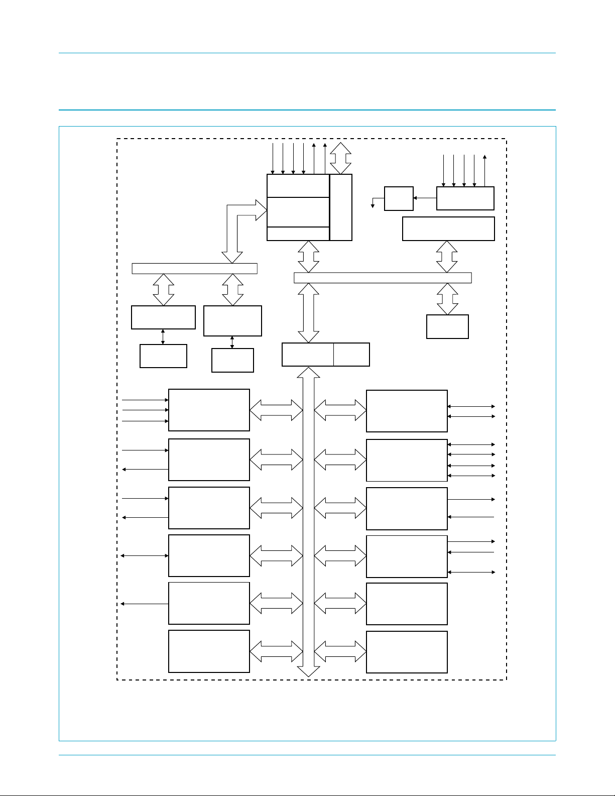
4. Block diagram
(1)
(1)
(1)
(1)
TDI
TCK
TMS
TRST
TEST/DEBUG
INTERFACE
ARM7TDMI-S
AHB BRIDGE
(1)
TDO
RTCK
LPC2104/2105/2106
system
MODULE
clock
EMULATION TRACE
Single-chip 32-bit microcontrollers
SS
DD
RST
V
V
XTAL2
XTAL1
PLL
VECTORED INTERRUPT
SYSTEM
FUNCTIONS
CONTROLLER
ARM7 LOCAL BUS
INTERNAL SRAM
CONTROLLER
16/32/64 kB
SRAM
EINT0*
EINT1*
EINT2*
CAP0..2*
MAT0..2*
CAP0..3*
MAT0..3*
GPIO (32 PINS)
INTERNAL
FLASH
CONTROLLER
128 kB
FLASH
EXTERNAL
INTERRUPTS
CAPTURE/
COMPARE
TIMER 0
CAPTURE/
COMPARE
TIMER 1
GENERAL
PURPOSE I/O
AHB TO VPB
BRIDGE
(Advanced High-performance Bus)
APB
AMBA AHB
VPB
DIVIDER
(2)
I2C SERIAL
INTERFACE
SPI SERIAL
INTERFACE
UART0
UART1
AHB
DECODER
MODEM CONTROL
SCL*
SDA*
SCK*
MOSI*
MISO*
SSEL*
TxD*
RxD*
TxD*
RxD*
(6 PINS)*
PWM1..6*
*Shared with GPIO
PWM0
REAL TIME
CLOCK
WATCHDOG
TIMER
SYSTEM
CONTROL
002aaa412
(1) When test/debug interface is used, GPIO/other function sharing these pins are not available.
(2) APB with Ready signal.
Fig 1. Block diagram.
9397 750 14476
Product data Rev. 05 — 22 December 2004 3 of 32
© Koninklijke Philips Electronics N.V. 2004. All rights reserved.
Page 4
Philips Semiconductors
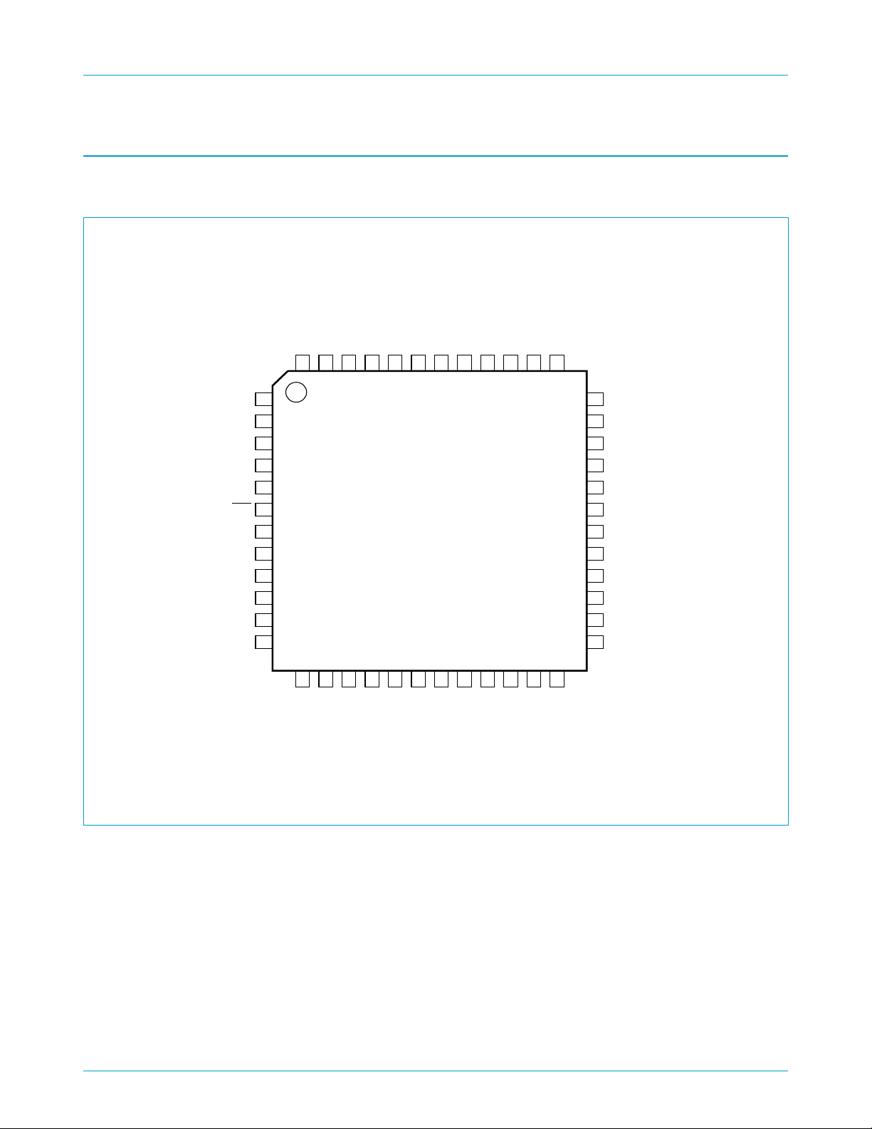
5. Pinning information
5.1 Pinning
LPC2104/2105/2106
Single-chip 32-bit microcontrollers
(I/O)
handbook, full pagewidth
P0.19/MAT1.2/TCK
P0.27/TRACEPKT0/TRST
P0.28/TRACEPKT1/TMS
P0.29/TRACEPKT2/TCK
P0.20/MAT1.3/TDI
P0.21/PWM5/TDO
V
(CORE)
DD1.8
RST
V
SS1
NC
P0.18/CAP1.3/TMS
P0.17/CAP1.2/TRST
P0.16/EINT0/MAT0.2
P0.15/RI1/EINT2
48
47
46
45
1
2
3
4
5
6
7
8
9
10
11
X1
12
X2
13
14
P0.0/TxD0/PWM1
P0.1/RxD0/PWM3
LPC2104/2105/2106
15
16
P0.31/EXTIN0/TDO
P0.30/TRACEPKT3/TDI
SS4
P0.14/DCD1/EINT1
V
NC
44
43
42
17
18
19
(I/O)
DD3-2
V
SS2
V
P0.2/SCL/CAP0.0
DD3-1
P0.13/DTR1/MAT1.1
V
P0.26/TRACESYNC
P0.25/PIPESTAT2
41
40
39
38
20
21
22
23
NC
P0.4/SCK/CAP0.1
P0.3/SDA/MAT0.0
P0.5/MISO/MAT0.1
P0.12/DSR1/MAT1.0
37
36
P0.11/CTS1/CAP1.1
35
P0.10/RTS1/CAP1.0
34
P0.24/PIPESTAT1
33
P0.23/PIPESTAT0
32
P0.22/TRACECLK
31
V
SS3
30
P0.9/RxD1/PWM6
29
P0.8/TxD1/PWM4
28
P0.7/SSEL/PWM2
27
DBGSEL
26
RTCK
25
NC
24
002aaa411
P0.6/MOSI/CAP0.2
Fig 2. Pinning.
9397 750 14476
Product data Rev. 05 — 22 December 2004 4 of 32
© Koninklijke Philips Electronics N.V. 2004. All rights reserved.
Page 5

Philips Semiconductors
LPC2104/2105/2106
Single-chip 32-bit microcontrollers
5.2 Pin description
Table 3: Pin description
Symbol Pin Type Description
P0.0 to P0.31 I/O Port 0: Port 0 is a 32-bit bi-directional I/O port with individual direction
controls for each bit. The operation of port 0 pins depends upon the pin
function selected via the Pin Connect Block.
13 I/O P0.0 — Port 0 bit 0.
O TxD0 — Transmitter output for UART 0.
O PWM1 — Pulse Width Modulator output 1.
14 I/O P0.1 — Port 0 bit 1.
I RxD0 — Receiver input for UART 0.
O PWM3 — Pulse Width Modulator output 3.
18 I/O P0.2 — Port 0 bit 2.
2
I/O SCL — I
I CAP0.0 — Capture input for Timer 0, channel 0.
21 I/O P0.3 — Port 0 bit 3.
I/O SDA — I
O MAT0.0 — Match output for Timer 0, channel 0.
22 I/O P0.4 — Port 0 bit 4.
I/O SCK — Serial clock. SPI clock output from master or input to slave.
I CAP0.1 — Capture input for Timer 0, channel 1.
23 I/O P0.5 — Port 0 bit 5.
I/O MISO — Master In Slave Out. Data input to SPI master or data output from
SPI slave.
O MAT0.1 — Match output for Timer 0, channel 1.
24 I/O P0.6 — Port 0 bit 6.
I/O MOSI — Master Out Slave In. Data output from SPI master or data input to
SPI slave.
I CAP0.2 — Capture input for Timer 0, channel 2.
28 I/O P0.7 — Port 0 bit 7.
I SSEL — Slave Select. Selects the SPI interface as a slave.
O PWM2 — Pulse Width Modulator output 2.
29 I/O P0.8 — Port 0 bit 8.
O TxD1 — Transmitter output for UART 1.
O PWM4 — Pulse Width Modulator output 4.
30 I/O P0.9 — Port 0 bit 9.
I RxD1 — Receiver input for UART 1.
O PWM6 — Pulse Width Modulator output 6.
C clock input/output. Open drain output (for I2C compliance).
2
C data input/output. Open drain output (for I2C compliance).
9397 750 14476
Product data Rev. 05 — 22 December 2004 5 of 32
© Koninklijke Philips Electronics N.V. 2004. All rights reserved.
Page 6

Philips Semiconductors
LPC2104/2105/2106
Single-chip 32-bit microcontrollers
Table 3: Pin description
Symbol Pin Type Description
35 I/O P0.10 — Port 0 bit 10.
36 I/O P0.11 — Port 0 bit 11.
37 I/O P0.12 — Port 0 bit 12.
41 I/O P0.13 — Port 0 bit 13.
44 I/O P0.14 — Port 0 bit 14.
45 I/O P0.15 — Port 0 bit 15.
46 I/O P0.16 — Port 0 bit 16.
47 I/O P0.17 — Port 0 bit 17.
48 I/O P0.18 — Port 0 bit 18.
1 I/O P0.19 — Port 0 bit 19.
2 I/O P0.20 — Port 0 bit 20.
3 I/O P0.21 — Port 0 bit 21.
32 I/O P0.22 — Port 0 bit 22.
33 I/O P0.23 — Port 0 bit 23.
34 I/O P0.24 — Port 0 bit 24.
…continued
O RTS1 — Request to Send output for UART 1.
I CAP1.0 — Capture input for Timer 1, channel 0.
I CTS1 — Clear to Send input for UART 1.
I CAP1.1 — Capture input for Timer 1, channel 1.
I DSR1 — Data Set Ready input for UART 1.
O MAT1.0 — Match output for Timer 1, channel 0.
O DTR1 — Data Terminal Ready output for UART 1.
O MAT1.1 — Match output for Timer 1, channel 1.
I DCD1 — Data Carrier Detect input for UART 1.
I EINT1 — External interrupt 1 input.
I RI1 — Ring Indicator input for UART 1.
O EINT2 — External interrupt 2 input.
I EINT0 — External interrupt 0 input.
O MAT0.2 — Match output for Timer 0, channel 2.
I CAP1.2 — Capture input for Timer 1, channel 2.
I TRST — Test Reset for JTAG interface, primary JTAG pin group.
I CAP1.3 — Capture input for Timer 1, channel 3.
I TMS — Test Mode Select for JTAG interface, primary JTAG pin group.
O MAT1.2 — Match output for Timer 1, channel 2.
I TCK — Test Clock for JTAG interface, primary JTAG pin group.
O MAT1.3 — Match output for Timer 1, channel 3.
I TDI — Test Data In for JTAG interface, primary JTAG pin group
O PWM5 — Pulse Width Modulator output 5.
O TDO — Test Data Out for JTAG interface, primary JTAG pin group.
O TRACECLK — Trace Clock. Standard I/O port with internal pull-up.
O PIPESTAT0 — Pipeline Status, bit 0. Standard I/O port with internal pull-up.
9397 750 14476
Product data Rev. 05 — 22 December 2004 6 of 32
© Koninklijke Philips Electronics N.V. 2004. All rights reserved.
Page 7

Philips Semiconductors
LPC2104/2105/2106
Single-chip 32-bit microcontrollers
Table 3: Pin description
…continued
Symbol Pin Type Description
O PIPESTAT1 — Pipeline Status, bit 1. Standard I/O port with internal pull-up.
38 I/O P0.25 — Port 0 bit 25.
O PIPESTAT2 — Pipeline Status, bit 2. Standard I/O port with internal pull-up.
39 I/O P0.26 — Port 0 bit 26.
O TRACESYNC — Trace Synchronization Standard I/O port with internal
pull-up.
8 I/O P0.27 — Port 0 bit 27.
O TRACEPKT0 — Trace Packet, bit 0. Standard I/O port with internal pull-up.
I TRST — Test Reset for JTAG interface, secondary JTAG pin group.
9 I/O P0.28 — Port 0 bit 28.
O TRACEPKT1 — Trace Packet, bit 1. Standard I/O port with internal pull-up.
I TMS — Test Mode Select for JTAG interface, secondary JTAG pin group
10 I/O P0.29 — Port 0 bit 29.
O TRACEPKT2 — Trace Packet, bit 2. Standard I/O port with internal pull-up.
I TCK — Test Clock for JTAG interface, secondary JTAG pin group.
15 I/O P0.30 — Port 0 bit 30.
O TRACEPKT3 — Trace Packet, bit 3. Standard I/O port with internal pull-up.
I TDI — Test Data In for JTAG interface, secondary JTAG pin group.
16 I/O P0.31 — Port 0 bit 31.
I EXTIN0 — External Trigger Input. Standard I/O port with internal pull-up.
O TDO — Test Data out for JTAG interface, secondary JTAG pin group.
RTCK 26 I/O Returned Test Clock output: Extra signal added to the JTAG port. Assists
debugger synchronization when processor frequency varies. Also used
during debug mode entry to select primary or secondary JTAG pins with the
48-pin package. Bi-directional pin with internal pull-up.
DBGSEL 27 I Debug Select: When LOW, the part operates normally. When HIGH, debug
mode is entered. Input pin with internal pull-down.
RST 6 I External Reset input: A LOW on this pin resets the device, causing I/O ports
and peripherals to take on their default states, and processor execution to
begin at address 0.
X1 11 I Input to the oscillator circuit and internal clock generator circuits.
X2 12 O Output from the oscillator amplifier.
V
V
SS1
DD1.8
- V
SS4
7, 19, 31, 43 I Ground: 0 V reference.
5I1.8 V Core Power Supply: This is the power supply voltage for internal
circuitry.
V
DD3
17, 40 I 3.3 V Pad Power Supply: This is the power supply voltage for the I/O ports.
NC 4, 20, 25, 42 - Not Connected: These pins are not connected in the 48 pin package.
9397 750 14476
Product data Rev. 05 — 22 December 2004 7 of 32
© Koninklijke Philips Electronics N.V. 2004. All rights reserved.
Page 8

Philips Semiconductors
6. Functional description
6.1 Architectural overview
The ARM7TDMI-S is a general purpose 32-bit microprocessor, which offers high
performance and very low power consumption. The ARM® architecture is based on
Reduced Instruction Set Computer (RISC) principles, and the instruction set and
related decode mechanism are much simpler than those of microprogrammed
Complex Instruction Set Computers. This simplicity results in a high instruction
throughput and impressive real-time interrupt response from a small and
cost-effective processor core.
Pipeline techniques are employed so that all parts of the processing and memory
systems can operate continuously. Typically, while one instruction is being executed,
its successor is being decoded, and a third instruction is being fetched from memory.
The ARM7TDMI-S processor also employs a unique architectural strategy known as
Thumb, which makes it ideally suited to high-volume applications with memory
restrictions, or applications where code density is an issue.
LPC2104/2105/2106
Single-chip 32-bit microcontrollers
The key idea behind Thumb is that of a super-reduced instruction set. Essentially, the
ARM7TDMI-S processor has two instruction sets:
• The standard 32-bit ARM set.
• A 16-bit Thumb set.
The Thumb set’s 16-bit instruction length allows it to approach twice the density of
standard ARM code while retaining most of the ARM’s performance advantage over a
traditional 16-bit processor using 16-bit registers. This is possible because Thumb
code operates on the same 32-bit register set as ARM code.
Thumb code is able to provide up to 65 % of the code size of ARM, and 160 % of the
performance of an equivalent ARM processor connected to a 16-bit memory system.
6.2 On-Chip Flash program memory
The LPC2104/2105/2106 incorporate a 128 kB Flash memory system. This memory
may be used for both code and data storage. Programming of the Flash memory may
be accomplished in several ways. It may be programmed In System via the serial
port. The application program may also erase and/or program the Flash while the
application is running, allowing a great degree of flexibility for data storage field
firmware upgrades, etc. When on-chip bootloader is used, 120 kB of Flash memory is
available for user code.
The LPC2104/2105/2106 Flash memory provides a minimum of 100,000 erase/write
cycles and 20 years of data retention.
6.3 On-Chip static RAM
On-Chip static RAM may be used for code and/or data storage. The SRAM may be
accessed as 8-bits, 16-bits, and 32-bits. The LPC2104 provides a 16 kB static RAM,
the LPC2105 provides a 32 kB static RAM, and the LPC2106 provides a 64 kB static
RAM.
9397 750 14476
Product data Rev. 05 — 22 December 2004 8 of 32
© Koninklijke Philips Electronics N.V. 2004. All rights reserved.
Page 9
Philips Semiconductors
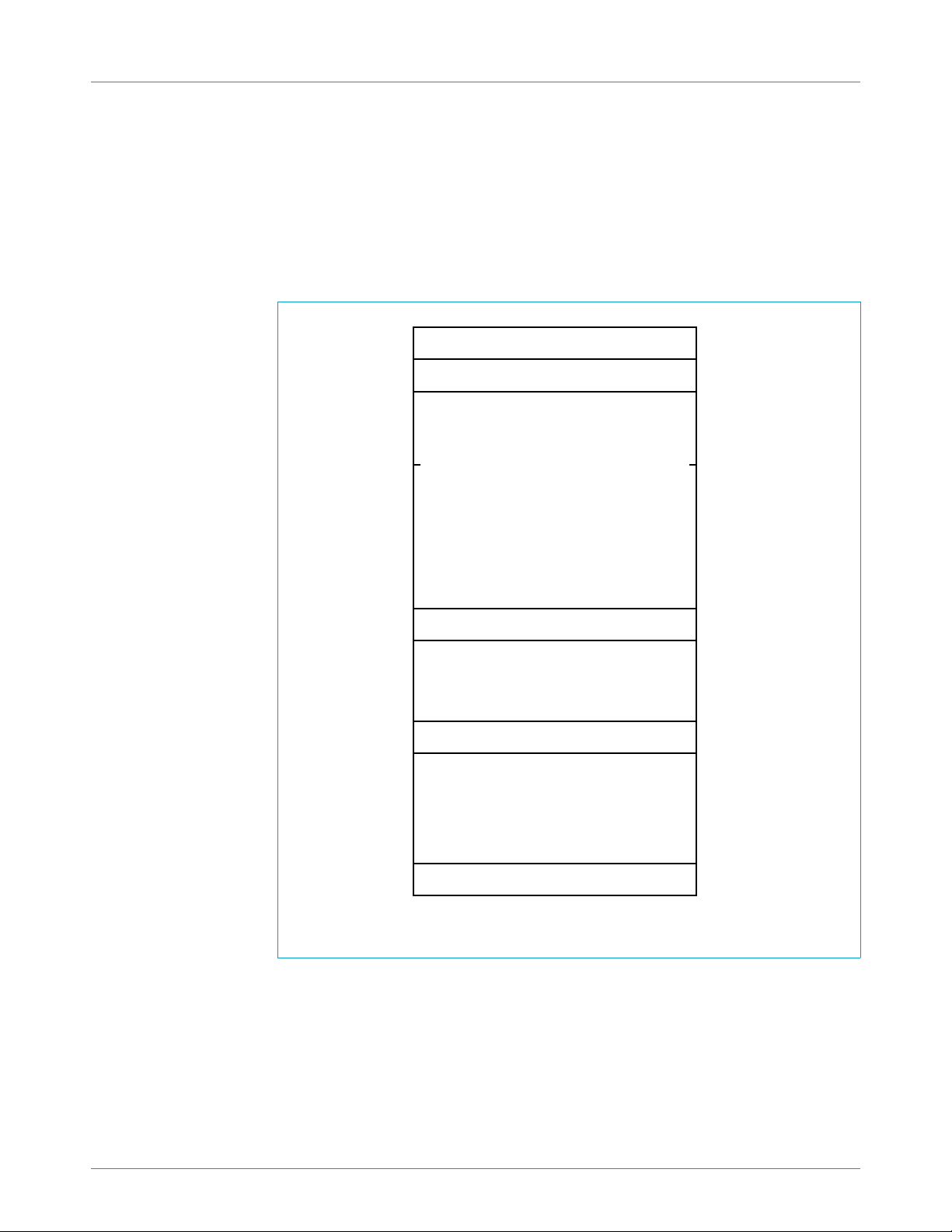
6.4 Memory map
The LPC2104, LPC2105 and LPC2106 memory maps incorporate several distinct
regions, as shown in the following figures.
In addition, the CPU interrupt vectors may be re-mapped to allow them to reside in
either Flash memory (the default) or on-chip static RAM. This is described in Section
6.17 “System control”.
LPC2104/2105/2106
Single-chip 32-bit microcontrollers
4.0 GB
3.75 GB
3.5 GB
3.0 GB
2.0 GB
1.0 GB
AHB PERIPHERALS
VPB PERIPHERALS
RESERVED ADDRESS SPACE
BOOT BLOCK (RE-MAPPED FROM
ON-CHIP FLASH MEMORY
RESERVED ADDRESS SPACE
16 KBYTE ON-CHIP STATIC RAM
0xFFFF FFFF
0xF000 0000
0xEFFF FFFF
0xE000 0000
0xDFFF FFFF
0xC000 0000
0x8000 0000
0x7FFF FFFF
0x7FFF E000
0x7FFF DFFF
0x4001 0000
0x4000 3FFF
0x4000 0000
0x3FFF FFFF
RESERVED ADDRESS SPACE
0x0002 0000
0.0 GB
128 KBYTE ON-CHIP FLASH MEMORY
0x0001 FFFF
0x0000 0000
002aaa415
Fig 3. LPC2104 memory map.
9397 750 14476
Product data Rev. 05 — 22 December 2004 9 of 32
© Koninklijke Philips Electronics N.V. 2004. All rights reserved.
Page 10
Philips Semiconductors
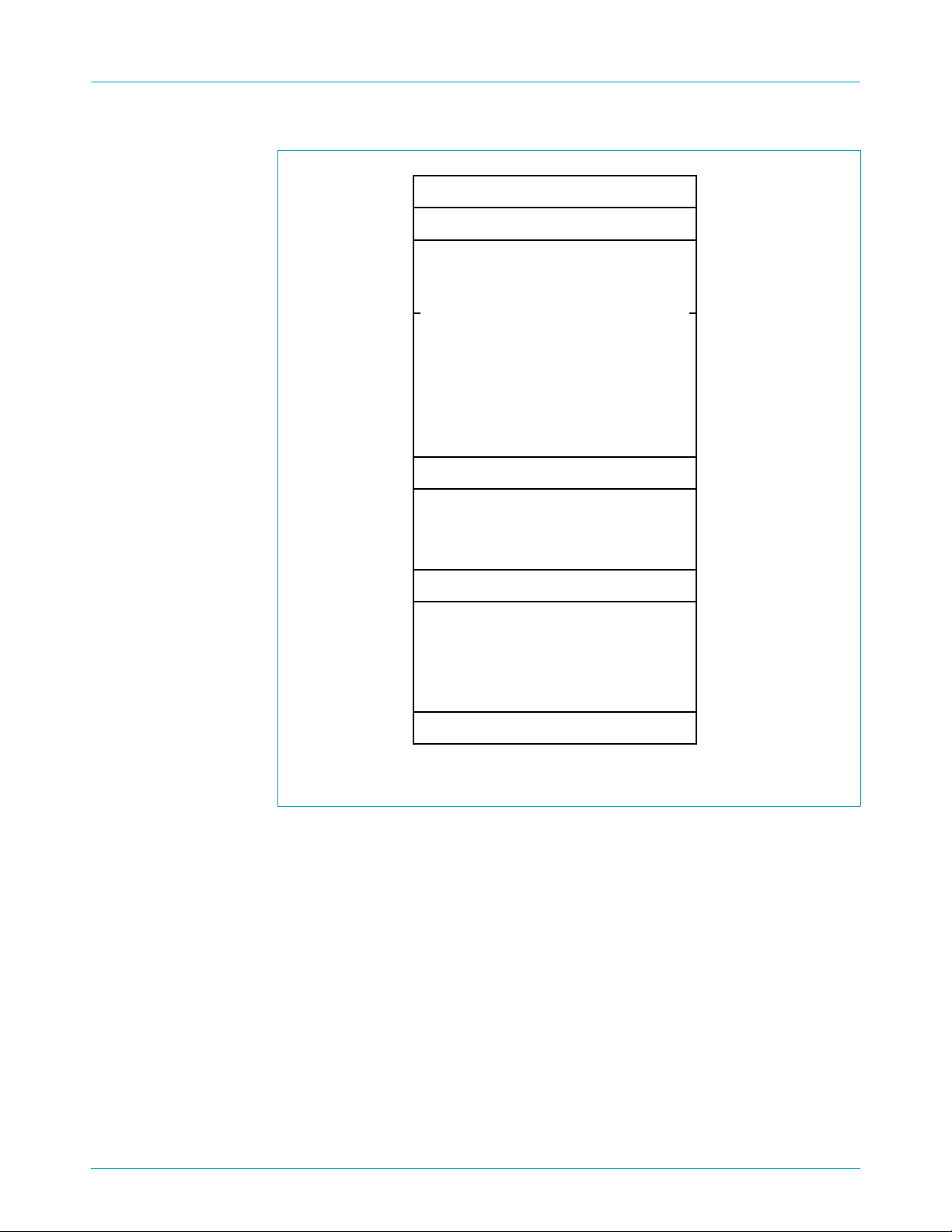
LPC2104/2105/2106
Single-chip 32-bit microcontrollers
4.0 GB
3.75 GB
3.5 GB
3.0 GB
2.0 GB
1.0 GB
AHB PERIPHERALS
VPB PERIPHERALS
RESERVED ADDRESS SPACE
BOOT BLOCK (RE-MAPPED FROM
ON-CHIP FLASH MEMORY
RESERVED ADDRESS SPACE
32 KBYTE ON-CHIP STATIC RAM
0xFFFF FFFF
0xF000 0000
0xEFFF FFFF
0xE000 0000
0xDFFF FFFF
0xC000 0000
0x8000 0000
0x7FFF FFFF
0x7FFF E000
0x7FFF DFFF
0x4000 8000
0x4000 7FFF
0x4000 0000
0x3FFF FFFF
0.0 GB
128 KBYTE ON-CHIP FLASH MEMORY
Fig 4. LPC2105 memory map.
RESERVED ADDRESS SPACE
0x0002 0000
0x0001 FFFF
0x0000 0000
002aaa414
9397 750 14476
© Koninklijke Philips Electronics N.V. 2004. All rights reserved.
Product data Rev. 05 — 22 December 2004 10 of 32
Page 11

Philips Semiconductors
LPC2104/2105/2106
Single-chip 32-bit microcontrollers
4.0 GB
3.75 GB
3.5 GB
3.0 GB
2.0 GB
1.0 GB
AHB PERIPHERALS
VPB PERIPHERALS
RESERVED ADDRESS SPACE
BOOT BLOCK (RE-MAPPED FROM
ON-CHIP FLASH MEMORY
RESERVED ADDRESS SPACE
64 KBYTE ON-CHIP STATIC RAM
0xFFFF FFFF
0xF000 0000
0xEFFF FFFF
0xE000 0000
0xDFFF FFFF
0xC000 0000
0x8000 0000
0x7FFF FFFF
0x7FFF E000
0x7FFF DFFF
0x4001 0000
0x4000 FFFF
0x4000 0000
0x3FFF FFFF
RESERVED ADDRESS SPACE
0x0002 0000
0.0 GB
128 KBYTE ON-CHIP FLASH MEMORY
0x0001 FFFF
0x0000 0000
002aaa413
Fig 5. LPC2106 memory map.
6.5 Interrupt controller
The Vectored Interrupt Controller (VIC) accepts all of the interrupt request inputs and
categorizes, them as FIQ, vectored IRQ, and non-vectored IRQ as defined by
programmablesettings.The programmable assignment scheme means that priorities
of interrupts from the various peripherals can be dynamically assigned and adjusted.
Fast Interrupt reQuest (FIQ) has the highest priority. If more than one request is
assigned to FIQ, the VIC combines the requests to produce the FIQ signal to the
ARM processor. The fastest possible FIQ latency is achieved when only one request
is classified as FIQ, because then the FIQ service routine can simply start dealing
with that device. But if more than one request is assigned to the FIQ class, the FIQ
service routine can read a word from the VIC that identifies which FIQ source(s) is
(are) requesting an interrupt.
9397 750 14476
© Koninklijke Philips Electronics N.V. 2004. All rights reserved.
Product data Rev. 05 — 22 December 2004 11 of 32
Page 12

Philips Semiconductors
Vectored IRQs have the middle priority. Sixteen of the interrupt requests can be
assigned to this category. Any of the interrupt requests can be assigned to any of the
16 vectored IRQ slots, among which slot 0 has the highest priority and slot 15 has the
lowest.
Non-vectored IRQs have the lowest priority.
The VIC combines the requests from all the vectored and non-vectored IRQs to
produce the IRQ signal to the ARM processor. The IRQ service routine can start by
reading a register from the VIC and jumping there. If any of the vectored IRQs are
requesting, the VIC provides the address of the highest-priority requesting IRQs
service routine, otherwise it provides the address of a defaultroutine that is shared by
all the non-vectored IRQs. The default routine can read another VIC register to see
what IRQs are active.
6.5.1 Interrupt sources
Table 4 lists the interrupt sources for each peripheral function. Each peripheral device
has one interrupt line connected to the Vectored Interrupt Controller, but may have
severalinternal interrupt flags. Individual interrupt flags may also represent more than
one interrupt source.
LPC2104/2105/2106
Single-chip 32-bit microcontrollers
Table 4: Interrupt sources
Block Flag(s) VIC channel #
WDT Watchdog Interrupt (WDINT) 0
- Reserved for software interrupts only 1
ARM Core Embedded ICE, DbgCommRx 2
ARM Core Embedded ICE, DbgCommTx 3
Timer 0 Match 0 to 3 (MR0, MR1, MR2, MR3)
Capture 0 to 3 (CR0, CR1, CR2, CR3)
Timer 1 Match 0 to 3 (MR0, MR1, MR2, MR3)
Capture 0 to 3 (CR0, CR1, CR2, CR3)
UART 0 Rx Line Status (RLS)
Transmit Holding Register empty (THRE)
Rx Data Available (RDA)
Character Time-out Indicator (CTI)
UART 1 Rx Line Status (RLS)
Transmit Holding Register empty (THRE)
Rx Data Available (RDA)
Character Time-out Indicator (CTI)
Modem Status Interrupt (MSI)
PWM0 Match 0 to 6 (MR0, MR1, MR2, MR3, MR4, MR5, MR6) 8
2
C SI (state change) 9
I
SPI SPIF, MODF 10
- reserved 11
PLL PLL Lock (PLOCK) 12
RTC RTCCIF (Counter Increment), RTCALF (Alarm) 13
4
5
6
7
9397 750 14476
Product data Rev. 05 — 22 December 2004 12 of 32
© Koninklijke Philips Electronics N.V. 2004. All rights reserved.
Page 13

Philips Semiconductors
LPC2104/2105/2106
Single-chip 32-bit microcontrollers
Table 4: Interrupt sources
Block Flag(s) VIC channel #
System Control External Interrupt 0 (EINT0) 14
System Control External Interrupt 1 (EINT1) 15
System Control External Interrupt 2 (EINT2) 16
…continued
6.6 Pin connect block
The pin connect block allows selected pins of the microcontroller to have more than
one function. Configuration registers control the multiplexers to allow connection
between the pin and the on chip peripherals. Peripherals should be connected to the
appropriate pins prior to being activated, and prior to any related interrupt(s) being
enabled. Activity of any enabled peripheral function that is not mapped to a related
pin should be considered undefined.
The Pin Control Module contains two registers as shown in Table 5.
Table 5:
Address Name Description Access
0xE002C000 PINSEL0 Pin function select register 0 Read/Write
0xE002C004 PINSEL1 Pin function select register 1 Read/Write
6.7 Pin function select register 0 (PINSEL0 - 0xE002C000)
The PINSEL0 register controls the functions of the pins as per the settings listed in
Table 6. The direction control bit in the IODIR register is effective only when the GPIO
function is selected for a pin. For other functions, direction is controlled automatically.
Settings other than those shown in Table 6 are reserved, and should not be used
Table 6: Pin function select register 0 (PINSEL0 - 0xE002C000)
PINSEL0 Pin name Value Function Value after Reset
1:0 P0.0 0 0 GPIO Port 0.0 0
0 1 TxD (UART 0)
1 0 PWM1
3:2 P0.1 0 0 GPIO Port 0.1 0
0 1 RxD (UART 0)
1 0 PWM3
5:4 P0.2 0 0 GPIO Port 0.2 0
2
0 1 SCL (I
1 0 Capture 0.0 (Timer 0)
7:6 P0.3 0 0 GPIO Port 0.3 0
01SDA (I
1 0 Match 0.0 (Timer 0)
9:8 P0.4 0 0 GPIO Port 0.4 0
0 1 SCK (SPI)
1 0 Capture 0.1 (Timer 0)
C)
2
C)
9397 750 14476
Product data Rev. 05 — 22 December 2004 13 of 32
© Koninklijke Philips Electronics N.V. 2004. All rights reserved.
Page 14

Philips Semiconductors
LPC2104/2105/2106
Single-chip 32-bit microcontrollers
Table 6: Pin function select register 0 (PINSEL0 - 0xE002C000)
PINSEL0 Pin name Value Function Value after Reset
11:10 P0.5 0 0 GPIO Port 0.5 0
0 1 MISO (SPI)
1 0 Match 0.1 (Timer 0)
13:12 P0.6 0 0 GPIO Port 0.6 0
0 1 MOSI (SPI)
1 0 Capture 0.2 (Timer 0)
15:14 P0.7 0 0 GPIO Port 0.7 0
0 1 SSEL (SPI)
1 0 PWM2
17:16 P0.8 0 0 GPIO Port 0.8 0
0 1 TxD UART 1
1 0 PWM4
19:18 P0.9 0 0 GPIO Port 0.9 0
0 1 RxD (UART 1)
1 0 PWM6
21:20 P0.10 0 0 GPIO Port 0.10 0
0 1 RTS (UART1)
1 0 Capture 1.0 (Timer 1)
23:22 P0.11 0 0 GPIO Port 0.11 0
0 1 CTS (UART1)
1 0 Capture 1.1 (Timer 1)
25:24 P0.12 0 0 GPIO Port 0.12 0
0 1 DSR (UART1)
1 0 Match 1.0 (Timer 1)
27:26 P0.13 0 0 GPIO Port 0.13 0
0 1 DTR (UART 1)
1 0 Match 1.1 (Timer 1)
29:28 P0.14 0 0 GPIO Port 0.14 0
0 1 CD (UART 1)
1 0 EINT1
31:30 P0.15 0 0 GPIO Port 0.15 0
0 1 RI (UART1)
1 0 EINT2
…continued
6.8 Pin function select register 1 (PINSEL1 - 0xE002C004)
The PINSEL1 register controls the functions of the pins as per the settings listed in
Table 7. The direction control bit in the IODIR register is effective only when the GPIO
function is selected for a pin. For other functions direction is controlled automatically.
Function control for the pins P0.17 - P0.31 is effectiveonly when the DBGSEL input is
pulled LOW during RESET.
9397 750 14476
Product data Rev. 05 — 22 December 2004 14 of 32
© Koninklijke Philips Electronics N.V. 2004. All rights reserved.
Page 15

Philips Semiconductors
Table 7: Pin function select register 1 (PINSEL1 - 0xE002C004)
PINSEL1 Pin Name Value Function Value after
1:0 P0.16 0 0 GPIO Port 0.16 0
3:2 P0.17 0 0 GPIO Port 0.17 0
5:4 P0.18 0 0 GPIO Port 0.18 0
7:6 P0.19 0 0 GPIO Port 0.19 0
9:8 P0.20 0 0 GPIO Port 0.20 0
11:10 P0.21 0 0 GPIO Port 0.21 0
13:12 P0.22 0 0 GPIO Port 0.22 0
15:14 P0.23 0 0 GPIO Port 0.23 0
17:16 P0.24 0 0 GPIO Port 0.24 0
19:18 P0.25 0 0 GPIO Port 0.25 0
21:20 P0.26 0 0 GPIO Port 0.26 0
23:22 P0.27 0 0 GPIO Port 0.27 0
25:24 P0.28 0 0 GPIO Port 0.28 0
27:26 P0.29 0 0 GPIO Port 0.29 0
29:28 P0.30 0 0 GPIO Port 0.30 0
31:30 P0.31 0 0 GPIO Port 0.31 0
LPC2104/2105/2106
Single-chip 32-bit microcontrollers
Reset
0 1 EINT0
1 0 Match 0.2 (Timer 0)
0 1 Capture 1.2 (Timer 1)
0 1 Capture 1.3 (Timer 1)
0 1 Match 1.2 (Timer 1)
0 1 Match 1.3 (Timer 1)
0 1 PWM5
0 1 TRST
0 1 TMS
0 1 TCK
0 1 TDI
0 1 TDO
6.9 General purpose parallel I/O
Device pins that are not connected to a specific peripheral function are controlled by
the GPIO registers. Pins may be dynamically configured as inputs or outputs.
Separate registers allow setting or clearing any number of outputs simultaneously.
The value of the output register may be read back, as well as the current state of the
port pins.
6.9.1 Features
• Direction control of individual bits.
• Separate control of output set and clear.
• All I/O default to inputs after reset.
9397 750 14476
Product data Rev. 05 — 22 December 2004 15 of 32
© Koninklijke Philips Electronics N.V. 2004. All rights reserved.
Page 16

Philips Semiconductors
6.10 UARTs
The LPC2104, LPC2105 and LPC2106 each contain two UARTs. One UART
provides a full modem control handshake interface, the other provides only transmit
and receive data lines.
6.10.1 Features
• 16 byte Receive and Transmit FIFOs.
• Register locations conform to ‘550 industry standard.
• Receiver FIFO trigger points at 1, 4, 8, and 14 bytes
• Built-in baud rate generator.
• Standard modem interface signals included on UART 1.
6.11 I2C serial I/O controller
I2C is a bi-directional bus for inter-IC control using only two wires: a serial clock line
(SCL), and a serial data line (SDA). Each device is recognized by a unique address
and can operate as either a receiver-only device (e.g. an LCD driver or a transmitter
with the capability to both receive and send information (such as memory).
Transmitters and/or receivers can operate in either master or slave mode, depending
on whether the chip has to initiate a data transfer or is only addressed. I2C is a
multi-master bus, it can be controlled by more than one bus master connected to it.
LPC2104/2105/2106
Single-chip 32-bit microcontrollers
I2C implemented in LPC2104, LPC2105 and LPC2106 supports bit rate up to
400 kbit/s (Fast I2C).
6.11.1 Features
• Standard I
• Easy to configure as Master, Slave, or Master/Slave.
• Programmable clocks allow versatile rate control.
• Bidirectional data transfer between masters and slaves.
• Multi-master bus (no central master).
• Arbitration between simultaneously transmitting masters without corruption of
serial data on the bus.
• Serial clock synchronization allows devices with different bit rates to communicate
via one serial bus.
• Serial clock synchronization can be used as a handshake mechanism to suspend
and resume serial transfer.
• The I
2
C compliant bus interface.
2
C bus may be used for test and diagnostic purposes.
9397 750 14476
Product data Rev. 05 — 22 December 2004 16 of 32
© Koninklijke Philips Electronics N.V. 2004. All rights reserved.
Page 17

Philips Semiconductors
6.12 SPI serial I/O controller
The SPI is a full duplex serial interface, designed to be able to handle multiple
masters and slaves connected to a given bus. Only a single master and a single slave
can communicate on the interface during a given data transfer.During a data transfer
the master always sends a byte of data to the slave, and the slave always sends a
byte of data to the master.
6.12.1 Features
• Compliant with Serial Peripheral Interface (SPI) specification.
• Synchronous, Serial, Full Duplex, Communication.
• Combined SPI master and slave.
• Maximum data bit rate of one eighth of the input clock rate.
6.13 General purpose timers
The Timer is designed to count cycles of the peripheral clock (PCLK) and optionally
generate interrupts or perform other actions at specified timer values, based on four
match registers. It also includes four capture inputs to trap the timer value when an
input signal transitions, optionally generating an interrupt.
LPC2104/2105/2106
Single-chip 32-bit microcontrollers
6.13.1 Features
• A 32-bit Timer/Counter with a programmable 32-bit Prescaler.
• Up to four (TImer 1) and three (Timer 0) 32-bit capture channels, that can take a
snapshot of the timer value when an input signal transitions. A capture event may
also optionally generate an interrupt.
• Four 32-bit match registers that allow:
– Continuous operation with optional interrupt generation on match.
– Stop timer on match with optional interrupt generation.
– Reset timer on match with optional interrupt generation.
• Up to four (Timer 1) and three (Timer 0) external outputs corresponding to match
registers, with the following capabilities:
– Set LOW on match.
– Set HIGH on match.
– Toggle on match.
– Do nothing on match.
6.14 Watchdog timer
The purpose of the Watchdog is to reset the microcontroller within a reasonable
amount of time if it enters an erroneous state. When enabled, the Watchdog will
generate a system reset if the user program fails to ‘feed’ (or reload) the Watchdog
within a predetermined amount of time.
9397 750 14476
Product data Rev. 05 — 22 December 2004 17 of 32
© Koninklijke Philips Electronics N.V. 2004. All rights reserved.
Page 18

Philips Semiconductors
6.14.1 Features
• Internally resets chip if not periodically reloaded.
• Debug mode.
• Enabled by software but requires a hardware reset or a Watchdog reset/interrupt to
• Incorrect/Incomplete feed sequence causes reset/interrupt if enabled.
• Flag to indicate Watchdog reset.
• Programmable 32-bit timer with internal pre-scaler.
LPC2104/2105/2106
Single-chip 32-bit microcontrollers
be disabled.
• Selectable time period from (t
t
× 4.
pclk
6.15 Real time clock
The Real Time Clock (RTC) is designed to provide a set of counters to measure time
when normal or idle operating mode is selected. The RTC has been designed to use
little power, making it suitable for battery powered systems where the CPU is not
running continuously (Idle mode).
6.15.1 Features
• Measures the passage of time to maintain a calendar and clock.
• Ultra Low Power design to support battery powered systems.
• Provides Seconds, Minutes, Hours, Day of Month, Month, Year, Day of Week, and
Day of Year.
• Programmable Reference Clock Divider allows adjustment of the RTC to match
various crystal frequencies.
6.16 Pulse width modulator
The PWM is based on the standard Timer block and inherits all of its features,
although only the PWM function is pinned out on the LPC2104, LPC2105 and
LPC2106. The Timer is designed to count cycles of the peripheral clock (PCLK) and
optionally generate interrupts or perform other actions when specified timer values
occur,basedon sevenmatchregisters.It also includes four capture inputs to save the
timer value when an input signal transitions, and optionally generate an interrupt
when those events occur. The PWM function is in addition to these features, and is
based on match register events.
× 256 × 4) to (t
pclk
× 232× 4) in multiples of
pclk
The ability to separately control rising and falling edge locations allows the PWM to
be used for more applications. For instance, multi-phase motor control typically
requires three non-overlapping PWM outputs with individual control of all three pulse
widths and positions.
Two match registers can be used to provide a single edge controlled PWM output.
One match register (MR0) controls the PWM cycle rate, by resetting the count upon
match. The other match register controls the PWM edge position. Additional single
9397 750 14476
Product data Rev. 05 — 22 December 2004 18 of 32
© Koninklijke Philips Electronics N.V. 2004. All rights reserved.
Page 19

Philips Semiconductors
edge controlled PWM outputs require only one match register each, since the
repetition rate is the same for all PWM outputs. Multiple single edge controlled PWM
outputs will all have a rising edge at the beginning of each PWM cycle, when an MR0
match occurs.
Three match registers can be used to provide a PWM output with both edges
controlled. Again, the MR0 match register controls the PWM cycle rate. The other
match registers control the two PWM edge positions. Additional double edge
controlled PWM outputs require only two match registers each, since the repetition
rate is the same for all PWM outputs.
With double edge controlled PWM outputs, specific match registers control the rising
and falling edge of the output. This allows both positive going PWM pulses (when the
rising edge occurs prior to the falling edge), and negative going PWM pulses (when
the falling edge occurs prior to the rising edge).
6.16.1 Features
• Seven match registers allow up to six single edge controlled or three double edge
LPC2104/2105/2106
Single-chip 32-bit microcontrollers
controlled PWM outputs, or a mix of both types.
• The match registers also allow:
– Continuous operation with optional interrupt generation on match.
– Stop timer on match with optional interrupt generation.
– Reset timer on match with optional interrupt generation.
• Supports single edge controlled and/or double edge controlled PWM outputs.
Single edge controlled PWM outputs all go HIGH at the beginning of each cycle
unless the output is a constant LOW. Double edge controlled PWM outputs can
have either edge occur at any position within a cycle. This allows for both positive
going and negative going pulses.
• Pulse period and width can be any number of timer counts. This allows complete
flexibility in the trade-off between resolution and repetition rate. All PWM outputs
will occur at the same repetition rate.
• Double edge controlled PWM outputs can be programmed to be either positive
going or negative going pulses.
• Match register updates are synchronized with pulse outputs to prevent generation
of erroneous pulses. Software must “release” new match values before they can
become effective.
• May be used as a standard timer if the PWM mode is not enabled.
• A 32-bit Timer/Counter with a programmable 32-bit Prescaler.
9397 750 14476
Product data Rev. 05 — 22 December 2004 19 of 32
© Koninklijke Philips Electronics N.V. 2004. All rights reserved.
Page 20

Philips Semiconductors
6.17 System control
6.17.1 Crystal oscillator
The oscillator supports crystals in the range of 1 MHz to 30 MHz. The oscillator
output frequency is called FOSC and the ARM processor clock frequency is referred
to as cclk for purposes of rate equations, etc. FOSC and cclk are the same value
unless the PLL is running and connected. Refer to Section 6.17.2 “PLL” for additional
information.
6.17.2 PLL
The PLL accepts an input clock frequency in the range of 10 MHz to 25 MHz. The
input frequency is multiplied up into the range of 10 MHz to 60 MHz with a Current
Controlled Oscillator (CCO). The multiplier can be an integer value from 1 to 32 (in
practice, the multiplier value cannot be higher than 6 on this family of microcontrollers
due to the upper frequency limit of the CPU). The CCO operates in the range of
156 MHz to 320 MHz, so there is an additional divider in the loop to keep the CCO
within its frequency range while the PLL is providing the desired output frequency.
The output divider may be set to divide by 2, 4, 8, or 16 to produce the output clock.
Since the minimum output divider value is 2, it is insured that the PLL output has a
50 % duty cycle.The PLL is turned off and bypassed following a chip Reset and may
be enabled by software. The program must configure and activate the PLL, wait for
the PLL to Lock, then connect to the PLL as a clock source. The PLL settling time is
100 µs.
LPC2104/2105/2106
Single-chip 32-bit microcontrollers
6.17.3 Reset and wake-up timer
Reset has two sources on the LPC2104, LPC2105 and LPC2106: the RST pin and
Watchdog Reset. The RST pin is a Schmitt trigger input pin with an additional glitch
filter. Assertion of chip Reset by any source starts the Wake-up Timer (see Wake-up
Timer description below), causing the internal chip reset to remain asserted until the
external Reset is de-asserted, the oscillator is running, a fixed number of clocks have
passed, and the on-chip Flash controller has completed its initialization.
When the internal Reset is removed, the processor begins executing at address 0,
which is the Reset vector. At that point, all of the processor and peripheral registers
have been initialized to predetermined values.
The wake-up timer ensures that the oscillator and other analog functions required for
chip operation are fully functional before the processor is allowed to execute
instructions. This is important at power on, all types of Reset, and whenever any of
the aforementioned functions are turned off for any reason. Since the oscillator and
other functions are turned off during Power-down mode, any wake-up of the
processor from Power-down mode makes use of the Wake-up Timer.
The Wake-up Timer monitors the crystal oscillator as the means of checking whether
it is safe to begin code execution. When power is applied to the chip, or some event
caused the chip to exit Power-down mode, some time is required for the oscillator to
produce a signal of sufficient amplitude to drive the clock logic. The amount of time
depends on many factors, including the rate of VDD ramp (in the case of power on),
the type of crystal and its electrical characteristics (if a quartz crystal is used), as well
as any other external circuitry (e.g. capacitors), and the characteristics of the
oscillator itself under the existing ambient conditions.
9397 750 14476
Product data Rev. 05 — 22 December 2004 20 of 32
© Koninklijke Philips Electronics N.V. 2004. All rights reserved.
Page 21

Philips Semiconductors
6.17.4 External interrupt inputs
The LPC2104, LPC2105 and LPC2106 include three External Interrupt Inputs as
selectable pin functions. The External Interrupt Inputs can optionally be used to wake
up the processor from Power-down mode.
6.17.5 Memory Mapping Control
The Memory Mapping Control alters the mapping of the interrupt vectors that appear
beginning at address 0x00000000. Vectors may be mapped to the bottom of the
on-chip Flash memory, or to the on-chip static RAM. This allows code running in
different memory spaces to have control of the interrupts.
6.17.6 Power Control
The LPC2104, LPC2105 and LPC2106 support two reduced power modes: Idle
mode and Power-down mode. In Idle mode, execution of instructions is suspended
until either a Reset or interrupt occurs. Peripheral functions continue operation during
Idle mode and may generate interrupts to cause the processor to resume execution.
Idle mode eliminates power used by the processor itself, memory systems and
related controllers, and internal buses.
LPC2104/2105/2106
Single-chip 32-bit microcontrollers
In Power-down mode, the oscillator is shut down and the chip receives no internal
clocks. The processor state and registers, peripheral registers, and internal SRAM
values are preserved throughout Power-down mode and the logic levels of chip
output pins remain static. The Power-down mode can be terminated and normal
operation resumed by either a Reset or certain specific interrupts that are able to
function without clocks. Since all dynamic operation of the chip is suspended,
Power-down mode reduces chip power consumption to nearly zero.
A PowerControlforPeripherals feature allows individual peripherals to be turned off if
they are not needed in the application, resulting in additional power savings.
6.17.7 VPB bus
The VPB divider determines the relationship between the processor clock (CCLK)
and the clock used by peripheral devices (PCLK). The VPB divider serves two
purposes. The first is to provide peripherals with the desired PCLK via VPB bus so
that they can operate at the speed chosen for the ARM processor. In order to achieve
this, the VPB bus may be slowed down to1⁄2 to1⁄4 of the processor clock rate.
Because the VPB bus must work properly at power-up (and its timing cannot be
altered if it does not work since the VPB divider control registers reside on the VPB
bus), the default condition at reset is for the VPB bus to run at1⁄4 of the processor
clock rate. The second purpose of the VPB divider is to allow power savings when an
application does not require any peripherals to run at the full processor rate. Because
the VPB divider is connected to the PLL output, the PLL remains active (if it was
running) during Idle mode.
6.18 Emulation and debugging
The LPC2104, LPC2105 and LPC2106 support emulation and debugging via a JTAG
serial port. A trace port allows tracing program execution. Each of these functions
requires a trade-off of debugging features versus device pins. Because the LPC2104,
9397 750 14476
Product data Rev. 05 — 22 December 2004 21 of 32
© Koninklijke Philips Electronics N.V. 2004. All rights reserved.
Page 22

Philips Semiconductors
LPC2105 and LPC2106 are provided in a small package, there is no room for
permanently assigned JTAGor Trace pins. An alternate JTAG port allows an option to
debug functions assigned to the pins used by the primary JTAG port.
6.18.1 Embedded ICE
Standard ARM EmbeddedICE™ logic provides on-chip debug support. The
debugging of the target system requires a host computer running the debugger
software and an EmbeddedICE protocol convertor. EmbeddedICE protocol convertor
converts the Remote Debug Protocol commands to the JTAG data needed to access
the ARM core.
The ARM core has a Debug Communication Channel function in-built. The debug
communication channel allows a program running on the target to communicate with
the host debugger or another separate host without stopping the program flow or
even entering the debug state. The debug communication channel is accessed as a
co-processor 14 by the program running on the ARM7TDMI-S core. The debug
communication channel allows the JTAG port to be used for sending and receiving
data without affecting the normal program flow. The debug communication channel
data and control registers are mapped in to addresses in the EmbeddedICE logic.
LPC2104/2105/2106
Single-chip 32-bit microcontrollers
6.18.2 Embedded trace
Since the LPC2104, LPC2105 and LPC2106 have significant amounts of on-chip
memory, it is not possible to determine how the processor core is operating simply by
observing the external pins. The Embedded Trace Macrocell provides real-time trace
capability for deeply embedded processor cores. It outputs information about
processor execution to the trace port.
The ETM is connected directly to the ARM core and not to the main AMBA system
bus. It compresses the trace information and exports it through a narrow trace port.
An external trace port analyzer must capture the trace information under software
debugger control. Instruction trace (or PC trace) shows the flow of execution of the
processor and provides a list of all the instructions that were executed. Instruction
trace is significantly compressed by only broadcasting branch addresses as well as a
set of status signals that indicate the pipeline status on a cycle by cycle basis. Trace
information generation can be controlled by selecting the trigger resource. Trigger
resources include address comparators, counters and sequencers. Since trace
information is compressed the software debugger requires a static image of the code
being executed. Self-modifying code can not be traced because of this restriction.
6.18.3 RealMonitor™
RealMonitor is a configurable software module, developed by ARM Inc., which
enables real time debug. It is a lightweight debug monitor that runs in the background
while users debug their foreground application. It communicates with the host using
the DCC (Debug Communications Channel), which is present in the EmbeddedICE
logic. The LPC2104, LPC2105 and LPC2106 contain a specific configuration of
RealMonitor software programmed into the on-chip Flash memory.
9397 750 14476
Product data Rev. 05 — 22 December 2004 22 of 32
© Koninklijke Philips Electronics N.V. 2004. All rights reserved.
Page 23

Philips Semiconductors
7. Limiting values
LPC2104/2105/2106
Single-chip 32-bit microcontrollers
Table 8: Limiting values
In accordance with the Absolute Maximum Rating System (IEC 60134).
[1]
Symbol Parameter Conditions Min Max Unit
V
V
V
V
DD1.8
DD3
i
i
Supply voltage, internal rail −0.5 +2.5 V
Supply voltage, external rail −0.5 +3.6 V
DC input voltage, 5 V tolerant I/O
[2][3]
pins
DC input voltage, other I/O pins
[4][2]
−0.5 6.0 V
−0.5 V
DD3
+
V
0.5
I DC supply current per supply pin
I DC ground current per ground pin
T
stg
Storage temperature
[6]
P Power dissipation (based on
[5]
[5]
- 100 mA
- 100 mA
−65 150 °C
1.5 - W
package heat transfer, not device
power consumption)
[1] The following applies to the Limiting values:
a) Stresses above those listed under Limiting values may cause permanent damage to the device.
This is a stress rating only and functional operation of the device at these or any conditions other
than those described in Section 8 “Static characteristics” and Section 9 “Dynamic characteristics”
of this specification is not implied.
b) This product includes circuitry specifically designed for the protection of its internal devices from
the damaging effects of excessive static charge. Nonetheless, it is suggested that conventional
precautions be taken to avoid applying greater than the rated maximum.
c) Parameters are valid over operating temperature range unless otherwise specified. All voltages
are with respect to VSS unless otherwise noted.
[2] Including voltage on outputs in 3-state mode.
[3] Only valid when the V
[4] Not to exceed 4.6 V.
[5] The peak current is limited to 25 times the corresponding maximum current.
[6] Dependent on package type.
supply voltage is present.
DD3
9397 750 14476
Product data Rev. 05 — 22 December 2004 23 of 32
© Koninklijke Philips Electronics N.V. 2004. All rights reserved.
Page 24

Philips Semiconductors
LPC2104/2105/2106
Single-chip 32-bit microcontrollers
8. Static characteristics
Table 9: Static characteristics
T
=0°Cto+70°C for commercial, unless otherwise specified.
amb
Symbol Parameter Conditions Min Typ
V
DD1.8
V
DD3
Standard Port pins,
I
IL
I
IH
I
OZ
I
latchup
V
i
V
o
V
IH
V
IL
V
hys
V
OH
V
OL
I
OH
I
OL
I
OH
I
OL
I
PD
I
PU
I
DD1.8
2
C pins
I
V
IH
V
IL
V
hys
V
OL
Supply voltage 1.65 1.8 1.95 V
External rail supply voltage 3.0 3.3 3.6 V
RST, RTCK, and DBGSEL
LOW level input current, no
Vi=0 - - 3 µA
pull-up
HIGH level input current, no
Vi=V
DD3
--3µA
pull down
3-state output leakage, no
Vo= 0, Vo=V
DD3
--3µA
pull-up/down
I/O latch-up current −(0.5V
T
< 125 °C
j
Input voltage
[2][3][4]
) < V < (1.5 V
DD3
DD3
)
100 - - mA
0 - 5.5 V
Output voltage, output active 0 - V
HIGH level input voltage 2.0 - - V
LOW level input voltage - - 0.8 V
Hysteresis voltage - 0.4 - V
HIGH level output voltage
LOW level output voltage
HIGH level output current
LOW level output current
HIGH level short circuit
[6]
current
LOW level short circuit
[6]
current
Pull-downcurrent(appliesto
[5]
IOH= −4 mA V
[5]
IOL= −4 mA - - 0.4 V
[5]
VOH=V
[5]
VOL= 0.4 V 4 - - mA
− 0.4 V −4--mA
DD3
− 0.4 - - V
DD3
VOH=0 - - −45 mA
VOL=V
Vi=5V
DD3
[7]
- - 50 mA
20 50 100 µA
DBGSEL)
Pull-up current (applies to
P0.22 - P0.31)
Active Mode V
Vi=0 −25 −50 −65 µA
< Vi< 5 V
V
DD3
DD1.8
=25°C, code
T
amb
[7]
= 1.8 V, cclk = 60 MHz,
000µA
-30-mA
while(1){}
executed from FLASH, no active
peripherals
Power-down Mode V
HIGH level input voltage V
LOW level input voltage V
Hysteresis voltage V
LOW level output voltage
[5]
= 1.8 V, T
DD1.8
= 1.8 V, T
V
DD1.8
is from 4.5 V to 5.5 V 0.7V
TOL
is from 4.5 V to 5.5 V - - 0.3 V
TOL
is from 4.5 V to 5.5 V - 0.5 V
TOL
= +25 °C, - 10 - µA
amb
= +85 °C - 50 500 µA
amb
TOL
--V
IOL= 3 mA - - 0.4 V
[1]
Max Unit
DD3
TOL
-V
TOL
V
V
9397 750 14476
Product data Rev. 05 — 22 December 2004 24 of 32
© Koninklijke Philips Electronics N.V. 2004. All rights reserved.
Page 25

Philips Semiconductors
LPC2104/2105/2106
Single-chip 32-bit microcontrollers
SS
…continued
Vi=V
= 5 V - 10 22 µA
V
i
DD3
[1]
Max Unit
-24µA
Table 9: Static characteristics
T
=0°Cto+70°C for commercial, unless otherwise specified.
amb
Symbol Parameter Conditions Min Typ
I
lkg
Input leakage to V
Oscillator pins
X1 input Voltages 0 - V
X2 output Voltages 0 - V
DD1.8
DD1.8
On-chip Flash program memory
endurance (write and erase) 100,000 - - cycles
data retention 20 - - years
[1] Typical ratings are not guaranteed. The values listed are at room temperature (+25 ˚C), nominal supply voltages. Pin capacitance is
characterized but not tested.
[2] Including voltage on outputs in 3-state mode.
[3] V
[4] 3-state outputs go into 3-state mode when V
[5] Accounts for 100 mV voltage drop in all supply lines.
[6] Only allowed for a short time period.
[7] Minimum condition for Vi= 4.5 V, maximum condition for Vi= 5.5 V.
supply voltages must be present.
DD3
is grounded.
DD3
9397 750 14476
Product data Rev. 05 — 22 December 2004 25 of 32
© Koninklijke Philips Electronics N.V. 2004. All rights reserved.
Page 26

Philips Semiconductors
9. Dynamic characteristics
LPC2104/2105/2106
Single-chip 32-bit microcontrollers
Table 10: Characteristics
T
=0°Cto+70°C for commercial,−40°C to +85°C for industrial, V
amb
DD1.8
, V
over specified ranges
DD3
Symbol Parameter Conditions Min Typ
External Clock
f
osc
Oscillator frequency supplied by an
1 - 50 MHz
external oscillator (signal generator)
External clockfrequencysuppliedby
1 - 30 MHz
an external crystal oscillator
External clock frequency if on-chip
10 - 25 MHz
PLL is used
External clock frequency if ISP is
10 - 25 MHz
used for initial code download
t
C
t
CHCX
t
CLCX
t
CLCH
t
CHCL
External oscillator clock period 20 - 1000 ns
Clock HIGH time tc× 0.4 - - ns
Clock LOW time tc× 0.4 - - ns
Clock rise time - - 5 ns
Clock fall time - - 5 ns
Port Pins
t
RISE
Port output rise time (except P0.2,
---ns
P0.3)
t
FALL
Port output fall time (except P0.2,
---ns
P0.3)
2
I
C pins
t
f
Output fall time from VIH to V
IL
20 +
0.1 × C
--ns
[2]
b
[1]
[1]
Max Unit
[1] Parameters are valid over operating temperature range unless otherwise specified.
[2] Bus capacitance Cb in pF, from 10 pF to 400 pF.
9397 750 14476
Product data Rev. 05 — 22 December 2004 26 of 32
© Koninklijke Philips Electronics N.V. 2004. All rights reserved.
Page 27

Philips Semiconductors
9.1 Timing
Fig 6. External clock timing.
LPC2104/2105/2106
Single-chip 32-bit microcontrollers
V
- 0.5 V
DD
0.45 V
0.2 V
0.2 V
DD
DD
t
CHCL
+ 0.9
- 0.1 V
t
CLCX
t
C
t
CHCX
t
CLCH
002aaa416
9397 750 14476
© Koninklijke Philips Electronics N.V. 2004. All rights reserved.
Product data Rev. 05 — 22 December 2004 27 of 32
Page 28

Philips Semiconductors
10. Package outline
LPC2104/2105/2106
Single-chip 32-bit microcontrollers
LQFP48: plastic low profile quad flat package; 48 leads; body 7 x 7 x 1.4 mm
c
y
X
36
37
pin 1 index
48
25
24
Z
E
e
w M
b
p
13
A
H
E
E
A
2
A
SOT313-2
(A )
A
1
L
3
θ
L
p
1
e
DIMENSIONS (mm are the original dimensions)
A
UNIT
mm
Note
1. Plastic or metal protrusions of 0.25 mm maximum per side are not included.
OUTLINE
VERSION
SOT313-2 MS-026136E05
A1A2A3b
max.
0.20
1.6
0.05
1.45
1.35
IEC JEDEC JEITA
b
p
0.25
w M
D
H
D
p
0.27
0.17
12
Z
D
B
0 2.5 5 mm
(1)
(1) (1)(1)
cE
D
7.1
0.18
0.12
7.1
6.9
6.9
REFERENCES
v M
v M
scale
H
eHELL
9.15
0.5
8.85
detail X
A
B
Zywv θ
Z
0.95
0.55
D
E
0.95
7
0.55
0
ISSUE DATE
00-01-19
03-02-25
o
o
0.75
0.45
p
0.12 0.10.21
EUROPEAN
PROJECTION
D
9.15
8.85
Fig 7. SOT313-2 (LQFP48).
9397 750 14476
Product data Rev. 05 — 22 December 2004 28 of 32
© Koninklijke Philips Electronics N.V. 2004. All rights reserved.
Page 29

Philips Semiconductors
HVQFN48: plastic thermal enhanced very thin quad flat package; no leads;
48 terminals; body 7 x 7 x 0.85 mm
A
D
terminal 1
index area
B
E
LPC2104/2105/2106
Single-chip 32-bit microcontrollers
SOT619-1
A
A
1
detail X
c
e
1
D
D
5.25
4.95
h
h
1/2 e
b
25
1/2 e
36
37
0 2.5 5 mm
scale
(1)
E
E
h
7.1
5.25
4.95
0.51
6.9
REFERENCES
e
13 24
L
12
E
h
1
terminal 1
index area
DIMENSIONS (mm are the original dimensions)
(1)
A
UNIT
mm
Note
1. Plastic or metal protrusions of 0.075 mm maximum per side are not included.
OUTLINE
VERSION
SOT619-1 MO-220 - - -- - -
max.
A
0.05
0.00
48
(1)
c
b
1
0.30
0.18
D
7.1
0.2
6.9
IEC JEDEC JEITA
C
y
1
y
X
ISSUE DATE
01-08-08
02-10-18
v
M
ACCB
w
M
e
e
2
e
e
5.5
L
2
0.5
0.3
1
5.5
y
1
0.1v0.05
C
ye
w
0.05 0.1
EUROPEAN
PROJECTION
Fig 8. SOT619-1 (HVQFN48).
9397 750 14476
Product data Rev. 05 — 22 December 2004 29 of 32
© Koninklijke Philips Electronics N.V. 2004. All rights reserved.
Page 30

Philips Semiconductors
LPC2104/2105/2106
Single-chip 32-bit microcontrollers
11. Revision history
Table 11: Revision history
Rev Date CPCN Description
05 20041222 - Product data (9397 750 14476)
Modifications:
• Added new device LPC2106FBD48, removed device LPC2106BBD48.
• Section 6.2 “On-Chip Flash program memory” on page 8; updated text.
• Section 6.17.2 “PLL” on page 20; updated text.
• Section 6.17.7 “VPB bus” on page 21; updated text.
• Table 8 “Limiting values” on page 23; updated text.
• Table 9 “Static characteristics” on page 24; added On-chip Flash program memory specs.
04 20040205 - Product data (9397 750 12792); 853-2425 ECN 01-A15458f of 28 January 2004
03 20031007 - Product data (9397 750 12142); ECN 853-2425 30389 of 30 September 2003
02 20030611 - Product data (9397 750 11499); ECN 853-2425 29919 of 09 May 2003
01 20030425 - Product data (9397 750 11414); ECN 853-2425 29855 of 22 April 2003
9397 750 14476
Product data Rev. 05 — 22 December 2004 30 of 32
© Koninklijke Philips Electronics N.V. 2004. All rights reserved.
Page 31

Philips Semiconductors
12. Data sheet status
LPC2104/2105/2106
Single-chip 32-bit microcontrollers
Level Data sheet status
I Objective data Development This data sheet contains data from the objective specification for product development. Philips
II Preliminary data Qualification Thisdata sheetcontains data fromthe preliminary specification.Supplementary datawill be published
III Product data Production This data sheet contains data from the product specification. Philips Semiconductors reserves the
[1] Please consult the most recently issued data sheet before initiating or completing a design.
[2] The product status of the device(s) described in this data sheet may have changed since this data sheet was published. The latest information is available on the Internet at
URL http://www.semiconductors.philips.com.
[3] For data sheets describing multiple type numbers, the highest-level product status determines the data sheet status.
[1]
Product status
13. Definitions
Short-form specification — The data in a short-form specification is
extracted from a full data sheet with the same type number and title. For
detailed information see the relevant data sheet or data handbook.
Limiting values definition — Limiting values given are in accordance with
the Absolute Maximum Rating System (IEC 60134). Stress above one or
more of the limiting values may cause permanent damage to the device.
These are stress ratings only and operation of the device at these or at any
other conditions above those given in the Characteristics sections of the
specification is not implied. Exposure to limiting values for extended periods
may affect device reliability.
Application information — Applications that are described herein for any
of these products are for illustrative purposes only. Philips Semiconductors
make no representationor warranty that such applicationswill be suitable for
the specified use without further testing or modification.
[2][3]
Definition
Semiconductors reserves the right to change the specification in any manner without notice.
at alater date. Philips Semiconductorsreserves the right tochange the specification withoutnotice, in
order to improve the design and supply the best possible product.
right to makechanges at any timein order to improve the design, manufacturing and supply. Relevant
changes will be communicated via a Customer Product/Process Change Notification (CPCN).
performance. When the product is in full production (status ‘Production’),
relevant changes will be communicated via a Customer Product/Process
Change Notification (CPCN). Philips Semiconductors assumes no
responsibility or liability for the use of any of these products, conveys no
licence or title under any patent, copyright, or mask work right to these
products, and makes norepresentations orwarranties thatthese productsare
free frompatent, copyright, or mask workright infringement,unless otherwise
specified.
15. Licenses
Purchase of Philips I2C components
2
Purchase of Philips I
under the Philips’ I
2
I
C system provided the system conforms to the I2C
specification defined by Philips. This specification can be
ordered using the code 9398 393 40011.
C components conveys a license
2
C patent to use the components in the
14. Disclaimers
Life support — These products are not designed for use in life support
appliances, devices, or systems where malfunction of these products can
reasonably be expected to result in personal injury. Philips Semiconductors
customers using or selling these products for use in such applications do so
at their own risk and agree to fully indemnify Philips Semiconductors for any
damages resulting from such application.
Right to make changes — Philips Semiconductors reserves the right to
make changes in the products - including circuits, standard cells, and/or
software - described or contained herein in order to improve design and/or
16. Trademarks
ARM — is a registered trademark of ARM, Inc.
ARM7TDMI-S — is a trademark of ARM, Inc.
EmbeddedICE — is a trademark of ARM, Inc.
Embedded Trace Macrocell — is a trademark of ARM, Inc.
RealMonitor — is a trademark of ARM, Inc.
SPI — is a trademark of Motorola, Inc.
Thumb — is a trademark of ARM, Inc.
Contact information
For additional information, please visit http://www.semiconductors.philips.com.
For sales office addresses, send e-mail to: sales.addresses@www.semiconductors.philips.com. Fax: +31 40 27 24825
9397 750 14476
Product data Rev. 05 — 22 December 2004 31 of 32
© Koninklijke Philips Electronics N.V. 2004. All rights reserved.
Page 32

Philips Semiconductors
Contents
LPC2104/2105/2106
Single-chip 32-bit microcontrollers
1 General description. . . . . . . . . . . . . . . . . . . . . . 1
2 Features . . . . . . . . . . . . . . . . . . . . . . . . . . . . . . . 1
2.1 Key features . . . . . . . . . . . . . . . . . . . . . . . . . . . 1
3 Ordering information. . . . . . . . . . . . . . . . . . . . . 2
3.1 Ordering options . . . . . . . . . . . . . . . . . . . . . . . . 2
4 Block diagram . . . . . . . . . . . . . . . . . . . . . . . . . . 3
5 Pinning information. . . . . . . . . . . . . . . . . . . . . . 4
5.1 Pinning . . . . . . . . . . . . . . . . . . . . . . . . . . . . . . . 4
5.2 Pin description . . . . . . . . . . . . . . . . . . . . . . . . . 5
6 Functional description . . . . . . . . . . . . . . . . . . . 8
6.1 Architectural overview. . . . . . . . . . . . . . . . . . . . 8
6.2 On-Chip Flash program memory . . . . . . . . . . . 8
6.3 On-Chip static RAM . . . . . . . . . . . . . . . . . . . . . 8
6.4 Memory map. . . . . . . . . . . . . . . . . . . . . . . . . . . 9
6.5 Interrupt controller . . . . . . . . . . . . . . . . . . . . . 11
6.5.1 Interrupt sources. . . . . . . . . . . . . . . . . . . . . . . 12
6.6 Pin connect block . . . . . . . . . . . . . . . . . . . . . . 13
6.7 Pin function select register 0 (PINSEL0
- 0xE002C000). . . . . . . . . . . . . . . . . . . . . . . . 13
6.8 Pin function select register 1 (PINSEL1
- 0xE002C004). . . . . . . . . . . . . . . . . . . . . . . . 14
6.9 General purpose parallel I/O. . . . . . . . . . . . . . 15
6.9.1 Features . . . . . . . . . . . . . . . . . . . . . . . . . . . . . 15
6.10 UARTs . . . . . . . . . . . . . . . . . . . . . . . . . . . . . . 16
6.10.1 Features . . . . . . . . . . . . . . . . . . . . . . . . . . . . . 16
6.11 I
2
C serial I/O controller . . . . . . . . . . . . . . . . . . 16
6.11.1 Features . . . . . . . . . . . . . . . . . . . . . . . . . . . . . 16
6.12 SPI serial I/O controller. . . . . . . . . . . . . . . . . . 17
6.12.1 Features . . . . . . . . . . . . . . . . . . . . . . . . . . . . . 17
6.13 General purpose timers . . . . . . . . . . . . . . . . . 17
6.13.1 Features . . . . . . . . . . . . . . . . . . . . . . . . . . . . . 17
6.14 Watchdog timer. . . . . . . . . . . . . . . . . . . . . . . . 17
6.14.1 Features . . . . . . . . . . . . . . . . . . . . . . . . . . . . . 18
6.15 Real time clock . . . . . . . . . . . . . . . . . . . . . . . . 18
6.15.1 Features . . . . . . . . . . . . . . . . . . . . . . . . . . . . . 18
6.16 Pulse width modulator . . . . . . . . . . . . . . . . . . 18
6.16.1 Features . . . . . . . . . . . . . . . . . . . . . . . . . . . . . 19
6.17 System control . . . . . . . . . . . . . . . . . . . . . . . . 20
6.17.1 Crystal oscillator. . . . . . . . . . . . . . . . . . . . . . . 20
6.17.2 PLL . . . . . . . . . . . . . . . . . . . . . . . . . . . . . . . . . 20
6.17.3 Reset and wake-up timer . . . . . . . . . . . . . . . . 20
6.17.4 External interrupt inputs . . . . . . . . . . . . . . . . . 21
6.17.5 Memory Mapping Control. . . . . . . . . . . . . . . . 21
6.17.6 Power Control. . . . . . . . . . . . . . . . . . . . . . . . . 21
6.17.7 VPB bus . . . . . . . . . . . . . . . . . . . . . . . . . . . . . 21
6.18 Emulation and debugging. . . . . . . . . . . . . . . . 21
6.18.1 Embedded ICE . . . . . . . . . . . . . . . . . . . . . . . . 22
6.18.2 Embedded trace . . . . . . . . . . . . . . . . . . . . . . . 22
6.18.3 RealMonitor™. . . . . . . . . . . . . . . . . . . . . . . . . 22
7 Limiting values . . . . . . . . . . . . . . . . . . . . . . . . 23
8 Static characteristics . . . . . . . . . . . . . . . . . . . 24
9 Dynamic characteristics. . . . . . . . . . . . . . . . . 26
9.1 Timing . . . . . . . . . . . . . . . . . . . . . . . . . . . . . . 27
10 Package outline. . . . . . . . . . . . . . . . . . . . . . . . 28
11 Revision history . . . . . . . . . . . . . . . . . . . . . . . 30
12 Data sheet status. . . . . . . . . . . . . . . . . . . . . . . 31
13 Definitions . . . . . . . . . . . . . . . . . . . . . . . . . . . . 31
14 Disclaimers . . . . . . . . . . . . . . . . . . . . . . . . . . . 31
15 Licenses. . . . . . . . . . . . . . . . . . . . . . . . . . . . . . 31
16 Trademarks . . . . . . . . . . . . . . . . . . . . . . . . . . . 31
© Koninklijke Philips Electronics N.V. 2004.
Printed in the U.S.A.
All rights are reserved. Reproduction in whole or in part is prohibited without the prior
written consent of the copyright owner.
The information presented in this document does not form part of any quotation or
contract, is believed to be accurate and reliable and may be changed without notice. No
liability will be accepted by the publisher for any consequence of its use. Publication
thereof does not convey nor imply any license under patent- or other industrial or
intellectual property rights.
Date of release: 22 December 2004 Document order number: 9397 750 14476
 Loading...