

Philips L04E AC Service Manual
Colour Television Chassis
L04E
AC
E_14480_142.eps
260504
Contents Page Contents Page
1. Technical Specifications, Connections, and Chassis
Overview 2
2. Safety Instructions, Warnings, and Notes 4
3. Directions for Use 6
4. Mechanical Instructions 7
5. Service Modes, Error Codes, and Fault Finding 9
6. Block Diagrams, Test Point Overviews, and
Waveforms
Wiring Diagram 19
Block Diagram Supply and Deflection 20
Testpoint Overview Mono Carrier 21
Block Diagram Video 22
Testpoint Overview CRT, LTI & PIP Panel 23
Block Diagram Audio/Control 24
I2C and Supply Voltage Overview 25
7. Circuit Diagrams and PWB Layouts Diagram PWB
Mono Carrier: Power Supply (A1) 26 37-42
Mono Carrier: Diversity Table for A1 27 37-42
Mono Carrier: Deflection (A2) 28 37-42
Mono Carrier: Diversity Table for A2 29 37-42
Mono Carrier: Tuner IF (A3) 30 37-42
Mono Carrier: Hercules (A4) 31 37-42
Mono Carrier: Features & Connectivities (A5) 32 37-42
Mono Carrier: Class D - Audio Amplifier (A6) 33 37-42
Mono Carrier: Audio Amplifier (A7) 34 37-42
Mono Carrier: Rear I/O Scart (A8) 35 37-42
Mono Carrier: Front Control (A9) 36 37-42
Mono Carrier: DVD Power Supply (A10) 36 37-42
CRT Panel (B1) 43 45-46
CRT Panel: Eco Scavem (B2) 44 45-46
Side I/O + Headphone Panel (PV2) (D) 47 48
Side I/O + Headphone Panel (FL13) (D) 49 50
Top Control Panel (PV2) (E) 51 51
Top Control Panel (FL13) (E) 52 52
©
Copyright 2005 Philips Consumer Electronics B.V. Eindhoven, The Netherlands.
All rights reserved. No part of this publication may be reproduced, stored in a
retrieval system or transmitted, in any form or by any means, electronic,
mechanical, photocopying, or otherwise without the prior permission of Philips.
Power Supply PIP Panel (F1) 53 55-56
Tuner IF and Demodulator PIP Panel (F2) 54 55-56
Linearity & Panorama Panel (G) 57 57
LTI/CTI Interface Panel (H) 58 59
Front Interface Panel (FL13) (J) 60 60
Front Interface Panel (PV2) (J) 61 61
Front Interface and Keyboard Panel (J) 62 63
8. Alignments 65
9. Circuit Descriptions, Abbreviation List, and IC Data
Sheets 73
Abbreviation List 82
IC Data Sheets 84
10. Spare Parts List 86
11. Revision List 93
Published by WS 0572 TV Service Printed in the Netherlands Subject to modification EN 3122 785 16120
EN 2 L04E AC1.
Technical Specifications, Connections, and Chassis Overview
1. Technical Specifications, Connections, and Chassis Overview
Index of this chapter:
1.1 Technical Specifications
1.2 Connections
1.3 Chassis Overview
Notes:
• Described specifications are valid for the whole product
range.
• Figures below can deviate slightly from the actual situation,
due to different set executions.
1.1 Technical Specifications
1.1.1 Vision
Display type : DV-CRT-RF
:DV-CRT-FSQ
: DV-CRT-SF
Screen size : 21” (55 cm), 4:3
: 24” (61 cm), 16:9
: 25” (63 cm), 4:3
: 28” (70 cm), 4:3
: 29” (72 cm), 4:3
: 32” (82 cm), 16:9
Tuning system : PLL
TV Colour systems : PAL B/G, B/H, D/K, I
: SECAM
: SECAM B/G, D/K, L/L'
Video playback : NTSC
Channel selections : 100 presets
: UVSH
Aerial input : 75 ohm, Coax
:IEC-type
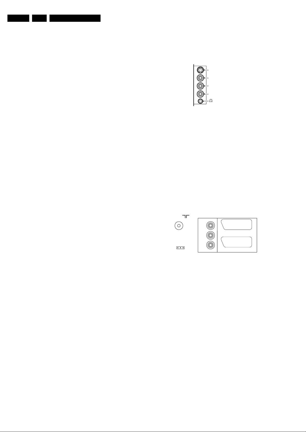
1.2.1 Side Connections
SIDE I/O
S-Video (optional)
Video
L
Audio
R
E_14480_111.eps
060504
Figure 1-1 Side I/O
S-Video: Y/C - In (Hosiden) (optional)
1 -Ground Gnd H
2 -Ground Gnd H
3 -Y 1 V_pp / 75 ohm j
4 -C 0.3 V_pp / 75 ohm j
Audio / Video In
Ye - Video (CVBS) 1 V_pp / 75 ohm jq
Wh - Audio - L 0.5 V_rms / 10 kohm jq
Rd - Audio - R 0.5 V_rms / 10 kohm jq
Bk - Headphone 8 - 600 Ohm / 4 mW ot
1.2.2 Rear Connections
AUDIO
75 Ohm
OUT
1.1.2 Sound
Sound systems : NICAM Stereo
Maximum power : 2x10/ 2x5 W_rms
(int.)
1.1.3 Miscellaneous
Power supply:
- Mains voltage : 220 - 240 V_ac
- Mains frequency : 50/60 Hz
Ambient conditions:
- Temperature range : +5 to +40 °C
- Maximum humidity : 90 % R.H.
Power consumption
- Normal operation : from 60 W (21”)
: to 91 W (32”)
- Standby : < 1 W
1.2 Connections
Note: The following connector colour abbreviations are used
(acc. to DIN/IEC 757): Bk= Black, Bu= Blue, Gn= Green, Gy=
Grey, Rd= Red, Wh= White, Ye= Yellow.
S
L
EXTERNAL 2
R
SERVICE
CONNECTOR
EXTERNAL 1
E_14480_151.eps
191005
Figure 1-2 Rear connections
Aerial In
- F-type Coax, 75 ohm D
Audio Out
Bk - Subwoofer - S Var. level (optional) kq
Wh - Audio - L 0.5 V_rms / 1 kohm kq
Rd - Audio - R 0.5 V_rms / 1 kohm kq
Technical Specifications, Connections, and Chassis Overview
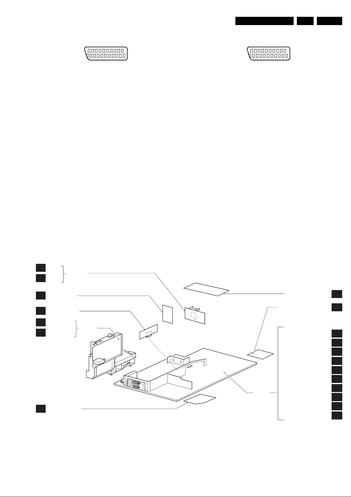
EN 3L04E AC 1.
External 1: RGB/YUV - In and CVBS - In/Out
20
21
2
1
E_06532_001.eps
050404
Figure 1-3 SCART connector EXT2
1 -Audio - R 0.5 V_rms / 1 kohm k
2 -Audio - R 0.5 V_rms / 10 kohm j
3 -Audio - L 0.5 V_rms / 1 kohm k
4 -Audio - gnd Ground H
5 -Blue - gnd Ground H
6 -Audio - L 0.5 V_rms / 10 kohm j
7 -Blue/U - in 0.7 V_pp / 75 ohm j
8 -CVBS - status 0 - 2 V: INT
4.5 - 7 V: EXT 16:9
9.5 - 12 V: EXT 4:3 j
9 -Green - gnd Ground H
10 - n.c.
11 - Green/Y - in 0.7 V_pp / 75 ohm j
12 - n.c.
13 - Red - gnd Ground H
14 - FBL - gnd Ground H
15 - Red/V - in 0.7 V_pp / 75 ohm j
16 - Status/FBL 0 - 0.4 V: INT
1 - 3 V: EXT / 75 ohm j
17 - Video Ground H
18 - Video Ground H
19 - CVBS - out 1 V_pp / 75 ohm k
20 - CVBS - in 1 V_pp / 75 ohm j
21 - Shielding Ground H
External 2: CVBS- In and SVHS - In
20
21
2
E_06532_001.eps
050404
1
Figure 1-4 SCART connector EXT1
1 -Audio - R 0.5 V_rms / 1 kohm k
2 -Audio - R 0.5 V_rms / 10 kohm j
3 -Audio - L 0.5 V_rms / 1 kohm k
4 -Audio - gnd Ground H
5 -Blue - gnd Ground H
6 -Audio - L 0.5 V_rms / 10 kohm j
7-n.c.
8 - CVBS - status 0 - 2 V: INT
4.5 - 7 V: EXT 16:9
9.5 - 12 V: EXT 4:3 j
9 - Green - gnd Ground H
10 - n.c.
11 - n.c.
12 - n.c.
13 - Red - gnd Ground H
14 - FBL - gnd Ground H
15 - YC-C - in 0.7 V_pp / 75 ohm j
16 - n.c.
17 - Video Ground H
18 - Video Ground H
19 - CVBS - out 1 V_pp / 75 ohm k
20 - Y/CVBS - in 1 V_pp / 75 ohm j
21 - Shielding Ground H
1.3 Chassis Overview
B1
CRT
ECO
B2
SCAVEM
SIDE AV PANEL +
D
HEADPHONE
LTI/CTI INTERFACE
H
PANEL
F1
POWER SUPPLY
TUNER IF &
F2
DEMODULATION
LINEARITY &
G
PANORAMA PANEL
CRT PANEL
PIP PANEL
MONO
CARRIER
TOP CONTROL PANEL
FRONT INTERFACE PANEL
POWER SUPPLY
LINE & FRAME DEFLECTION
TUNER IF
HERCULES
FEATURES & CONNECTIVITIES
CLASS D AUDIO AMPLIFIER
AUDIO AMPLIFIER
REAR I/O SCART
FRONT CONTROL
DVD POWER SUPPLY
E_14480_138.eps
E
J
A1
A2
A3
A4
A5
A6
A7
A8
A9
A10
131205
Figure 1-5 PWB location
EN 4 L04E AC2.
Safety Instructions, Warnings, and Notes
2. Safety Instructions, Warnings, and Notes
Index of this chapter:
2.1 Safety Instructions
2.2 Maintenance Instructions
2.3 Warnings
2.4 Notes
2.1 Safety Instructions
Safety regulations require that during a repair:
• Due to the chassis concept, a very large part of the circuitry
(incl. deflection) is 'hot'. Therefore, connect the set to the
mains via an isolation transformer.
• Replace safety components, indicated by the symbol h,
only by components identical to the original ones. Any
other component substitution (other than original type) may
increase risk of fire or electrical shock hazard.
• Wear safety goggles when you replace the CRT.
Safety regulations require that after a repair, you must return
the set in its original condition. Pay, in particular, attention to
the following points:
• General repair instruction: as a strict precaution, we advise
you to re-solder the solder connections through which the
horizontal deflection current is flowing. In particular this is
valid for the:
1. Pins of the line output transformer (LOT).
2. Fly-back capacitor(s).
3. S-correction capacitor(s).
4. Line output transistor.
5. Pins of the connector with wires to the deflection coil.
6. Other components through which the deflection current
flows.
• The maintenance inspection includes the following actions:
1. Perform the 'general repair instruction' noted above.
2. Clean the power supply and deflection circuitry on the
chassis.
3. Clean the picture tube panel and the neck of the picture
tube.
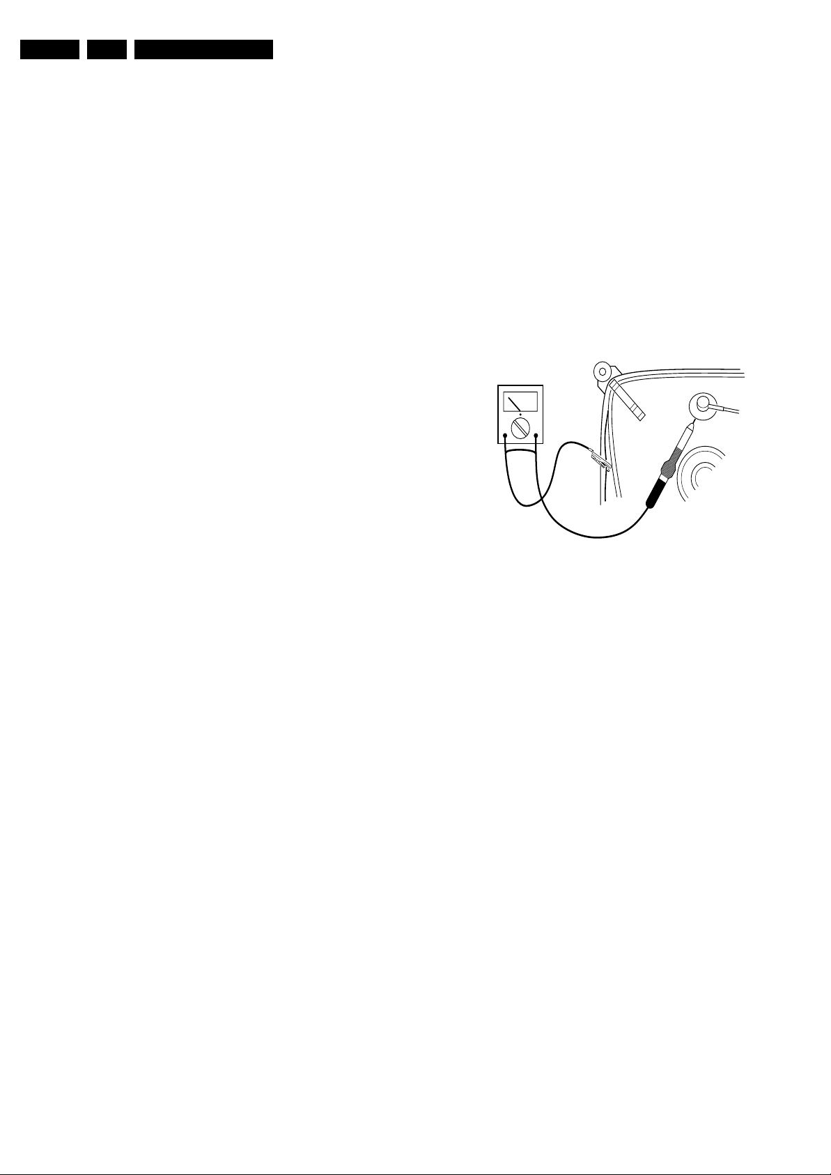
2.3 Warnings
• In order to prevent damage to ICs and transistors, avoid all
high voltage flash-overs. In order to prevent damage to the
picture tube, use the method shown in Fig. 2-1, to
discharge the picture tube. Use a high voltage probe and a
multi-meter (position V_dc). Discharge until the meter
reading is 0 V (after approx. 30 s).
V
Figure 2-1 Discharge picture tube
E_06532_007.eps
250304
Note: This re-soldering is advised to prevent bad connections
due to metal fatigue in solder connections, and is therefore only
necessary for television sets more than two years old.
• Route the wire trees and EHT cable correctly and secure
them with the mounted cable clamps.
• Check the insulation of the mains cord for external
damage.
• Check the strain relief of the mains cord for proper function,
to prevent the cord from touching the CRT, hot
components, or heat sinks.
• Check the electrical DC resistance between the mains plug
and the secondary side (only for sets that have an isolated
power supply). Do this as follows:
1. Unplug the mains cord and connect a wire between the
two pins of the mains plug.
2. Turn on the main power switch (keep the mains cord
unplugged!).
3. Measure the resistance value between the pins of the
mains plug and the metal shielding of the tuner or the
aerial connection of the set. The reading should be
between 4.5 MΩ and 12 MΩ.
4. Switch the TV 'off' and remove the wire between the
two pins of the mains plug.
• Check the cabinet for defects, to prevent the possibility of
the customer touching any internal parts.
2.2 Maintenance Instructions
We recommend a maintenance inspection carried out by
qualified service personnel. The interval depends on the usage
conditions:
• When a customer uses the set under normal
circumstances, for example in a living room, the
recommended interval is three to five years.
• When a customer uses the set in an environment with
higher dust, grease, or moisture levels, for example in a
kitchen, the recommended interval is one year.
• All ICs and many other semiconductors are susceptible to
electrostatic discharges (ESD, w). Careless handling
during repair can reduce life drastically. Make sure that,
during repair, you are connected with the same potential as
the mass of the set by a wristband with resistance. Keep
components and tools also at this potential. Available ESD
protection equipment:
– Complete kit ESD3 (small tablemat, wristband,
connection box, extension cable and ground cable)
4822 310 10671.
– Wristband tester 4822 344 13999.
• Together with the deflection unit and any multi-pole unit,
flat square picture tubes form an integrated unit. The
deflection and the multi-pole units are set optimally at the
factory. We do not recommend adjusting this unit during
repair.
• Be careful during measurements in the high voltage
section and on the picture tube.
• Never replace modules or other components while the unit
is 'on’.
• When you align the set, use plastic rather than metal tools.
This will prevent any short circuits and the danger of a
circuit becoming unstable.
2.4 Notes
2.4.1 General
• Measure the voltages and waveforms with regard to the
chassis (= tuner) ground (H), or hot ground (I), depending
on the tested area of circuitry.
• The voltages and waveforms shown in the diagrams are
indicative. Measure them in the Service Default Mode (see
chapter 5) with a colour bar signal and stereo sound (L: 3
kHz, R: 1 kHz unless stated otherwise) and picture carrier
at 475.25 MHz for PAL, or 61.25 MHz for NTSC (channel
3).
Safety Instructions, Warnings, and Notes
EN 5L04E AC 2.
• Where necessary, measure the waveforms and voltages
with (D) and without (E) aerial signal. Measure the
voltages in the power supply section both in normal
operation (G) and in standby (F). These values are
indicated by means of the appropriate symbols.
• The picture tube panel has printed spark gaps. Each spark
gap is connected between an electrode of the picture tube
and the Aquadag coating.
• The semiconductors indicated in the circuit diagram and in
the parts lists, are interchangeable per position with the
semiconductors in the unit, irrespective of the type
indication on these semiconductors.
• Manufactured under license from Dolby Laboratories.
“Dolby”, “Pro Logic” and the “double-D symbol”, are
trademarks of Dolby Laboratories
2.4.2 Schematic Notes
• All resistor values are in ohms and the value multiplier is
often used to indicate the decimal point location (e.g. 2K2
indicates 2.2 kohm).
• Resistor values with no multiplier may be indicated with
either an "E" or an "R" (e.g. 220E or 220R indicates 220
ohm).
• All capacitor values are given in micro-farads (µ= x 10
nano-farads (n= x 10
• Capacitor values may also use the value multiplier as the
decimal point indication (e.g. 2p2 indicates 2.2 pF).
• An "asterisk" (*) indicates component usage varies. Refer
to the diversity tables for the correct values.
• The correct component values are listed in the Electrical
Replacement Parts List. Therefore, always check this list
when there is any doubt.
2.4.3 Rework on BGA (Ball Grid Array) ICs
General
Although (LF)BGA assembly yields are very high, there may
still be a requirement for component rework. By rework, we
mean the process of removing the component from the PWB
and replacing it with a new component. If an (LF)BGA is
removed from a PWB, the solder balls of the component are
deformed drastically so the removed (LF)BGA has to be
discarded.
-9
), or pico-farads (p= x 10
-12
aligned under a microscope or magnifying glass. If this is not
possible, try to align the (LF)BGA with any board markers.
So as not to damage neighbouring components, it may be
necessary to reduce some temperatures and times.
More Information
For more information on how to handle BGA devices, visit this
URL: www.atyourservice.ce.philips.com (needs subscription,
not available for all regions). After login, select “Magazine”,
then go to “Repair downloads”. Here you will find Information
on how to deal with BGA-ICs.
2.4.4 Lead-free Solder
Philips CE is producing lead-free sets (PBF) from 1.1.2005
onwards.
Identification: The bottom line of a type plate gives a 14-digit
serial number. Digits 5 and 6 refer to the production year, digits
7 and 8 refer to production week (in example below it is 1991
week 18).
-6
),
).
E_06532_024.eps
230205
Figure 2-2 Serial number example
Regardless of the special lead-free logo (which is not always
indicated), one must treat all sets from this date onwards
according to the rules as described below.
P
b
Device Removal
As is the case with any component that is being removed, it is
essential when removing an (LF)BGA, that the board, tracks,
solder lands, or surrounding components are not damaged. To
remove an (LF)BGA, the board must be uniformly heated to a
temperature close to the reflow soldering temperature. A
uniform temperature reduces the risk of warping the PWB.
To do this, we recommend that the board is heated until it is
certain that all the joints are molten. Then carefully pull the
component off the board with a vacuum nozzle. For the
appropriate temperature profiles, see the IC data sheet.
Area Preparation
When the component has been removed, the vacant IC area
must be cleaned before replacing the (LF)BGA.
Removing an IC often leaves varying amounts of solder on the
mounting lands. This excessive solder can be removed with
either a solder sucker or solder wick. The remaining flux can be
removed with a brush and cleaning agent.
After the board is properly cleaned and inspected, apply flux on
the solder lands and on the connection balls of the (LF)BGA.
Note: Do not apply solder paste, as this has been shown to
result in problems during re-soldering.
Device Replacement
The last step in the repair process is to solder the new
component on the board. Ideally, the (LF)BGA should be
Figure 2-3 Lead-free logo
Due to lead-free technology some rules have to be respected
by the workshop during a repair:
• Use only lead-free soldering tin Philips SAC305 with order
code 0622 149 00106. If lead-free solder paste is required,
please contact the manufacturer of your soldering
equipment. In general, use of solder paste within
workshops should be avoided because paste is not easy to
store and to handle.
• Use only adequate solder tools applicable for lead-free
soldering tin. The solder tool must be able:
– To reach a solder-tip temperature of at least 400°C.
– To stabilise the adjusted temperature at the solder-tip.
– To exchange solder-tips for different applications.
• Adjust your solder tool so that a temperature of around
360°C - 380°C is reached and stabilised at the solder joint.
Heating time of the solder-joint should not exceed ~ 4 sec.
Avoid temperatures above 400°C, otherwise wear-out of
tips will increase drastically and flux-fluid will be destroyed.
To avoid wear-out of tips, switch “off” unused equipment or
reduce heat.
• Mix of lead-free soldering tin/parts with leaded soldering
tin/parts is possible but PHILIPS recommends strongly to
avoid mixed regimes. If this cannot be avoided, carefully
clean the solder-joint from old tin and re-solder with new
tin.

EN 6 L04E AC3.
Directions for Use
• Use only original spare-parts listed in the Service-Manuals.
Not listed standard material (commodities) has to be
purchased at external companies.
• Special information for lead-free BGA ICs: these ICs will be
delivered in so-called "dry-packaging" to protect the IC
against moisture. This packaging may only be opened
shortly before it is used (soldered). Otherwise the body of
the IC gets "wet" inside and during the heating time the
structure of the IC will be destroyed due to high (steam-)
pressure inside the body. If the packaging was opened
before usage, the IC has to be heated up for some hours
(around 90°C) for drying (think of ESD-protection!).
Do not re-use BGAs at all!
• For sets produced before 1.1.2005, containing leaded
soldering tin and components, all needed spare parts will
be available till the end of the service period. For the repair
of such sets nothing changes.
In case of doubt whether the board is lead-free or not (or with
mixed technologies), you can use the following method:
• Always use the highest temperature to solder, when using
SAC305 (see also instructions below).
3. Directions for Use
• De-solder thoroughly (clean solder joints to avoid mix of
two alloys).
Caution: For BGA-ICs, you must use the correct temperatureprofile, which is coupled to the 12NC. For an overview of these
profiles, visit the website www.atyourservice.ce.philips.com
(needs subscription, but is not available for all regions)
You will find this and more technical information within the
"Magazine", chapter "Repair downloads".
For additional questions please contact your local repair help
desk.
2.4.5 Practical Service Precautions
• It makes sense to avoid exposure to electrical shock.
While some sources are expected to have a possible
dangerous impact, others of quite high potential are of
limited current and are sometimes held in less regard.
• Always respect voltages. While some may not be
dangerous in themselves, they can cause unexpected
reactions - reactions that are best avoided. Before reaching
into a powered TV set, it is best to test the high voltage
insulation. It is easy to do, and is a good service precaution.
You can download this information from the following websites:
http://www.philips.com/support
http://www.p4c.philips.com
4. Mechanical Instructions
Index of this chapter:
4.1 Set Disassembly
4.2 Service Position
4.3 Assies/Panels Removal
4.4 Set Re-assembly
Notes:
• Figures below can deviate slightly from the actual situation,
due to different set executions.
• Make sure that both the ComPair connector and the UART
connector are shielded off with a piece of insulating tape
after repair for ESD reasons. Place this tape over the holes
in the rear cover of the set.
4.1 Set Disassembly
Mechanical Instructions
EN 7L04E AC 4.
1
Warning: Be sure to disconnect the AC power from the set
before opening it.
4.1.1 Rear Cover
1. Remove all fixation screws of the rear cover (do not forget
the screws that hold the rear connection panel).
2. Pull the rear cover backwards to remove it.
4.2 Service Position
Before placing the Mono Carrier in its service position, remove
the Front Interface assy/panel (see paragraph “Front Interface
Assy/Panel removal”), the Side AV assy/panel (see paragraph
“Side AV Assy/Panel removal”) and the PIP assy/panel (if
exists) (see paragraph “PIP Assy/Panel removal”).
2
A
3
4
E_14480_048.eps
B
110204
Figure 4-1 Service position Mono Carrier
1. Disconnect the degaussing coil [1].
2. Release the two fixation clamps (at the mid left and mid
right side of the bracket), and remove the bracket from the
bottom tray, by pulling it backwards [2].
3. Turn the chassis tray 90 degrees counter clockwise.
4. Move the panel bracket somewhat to the left and flip it 90
degrees [3], with the components towards the CRT.
5. Turn the panel bracket with the rear I/O toward the CRT.
6. Place the hook of the tray in the fixation hole of the cabinet
bottom [4] and secure it.
EN 8 L04E AC4.
Mechanical Instructions
4.3 Assies/Panels Removal
4.3.1 Front Interface Assy/Panel Removal
1
2
3
Figure 4-2 Front interface assy/panel removal
1. Remove the complete module from the bottom plate, by
pulling the two fixation clamps upward [1], while sliding the
module away from the CRT [2].
Note: these clamps are difficult to access.
2. Release the two fixation clamps [3] at the side of the
bracket, and lift the panel out of the bracket (it hinges at
one side).
1
3
E_14480_049.eps
110204
2. Push the assy a little bit upwards, and then pull it
backwards to release it from the front hinge.
3. Lift the panel from its bracket, while releasing the four
fixation clamps.
4.3.5 Linearity Assy/Panel Removal
2
Figure 4-4 Linearity assy/panel removal
1. Release the two fixation clamps [1] to lift the panel out of
the bracket [2].
4.3.6 PIP Assy/Panel Removal
1
1
E_14480_051.eps
270204
4.3.2 Side AV Assy/Panel Removal
E_14480_050.eps
170204
Figure 4-3 Side AV assy/panel removal
1. Remove the two fixation screws, and remove the complete
Side AV assembly.
2. Release the two fixation clamps, and lift the panel out of the
bracket.
4.3.3 LTI/CTI Interface Panel Removal
1. Release the two fixation clamps to lift the panel out of the
bracket.
4.4 Set Re-assembly
To re-assemble the whole set, do all processes in reverse
order.
Note: before you mount the rear cover, perform the following
checks:
1. Check whether the AC power cord is mounted correctly in
its guiding brackets.
2. Check whether all cables are replaced in their original
position
Remove the LTI/CTI Interface panel from the Mono Carrier, by
disconnecting it from connector 1212.
4.3.4 Top Control Assy/Panel Removal
Notes:
• PV02 styling: assy is mounted in the front cabinet;
• FL13B styling: assy is mounted in the rear cover.
1. Remove the two fixation screws.
Service Modes, Error Codes, and Fault Finding
5. Service Modes, Error Codes, and Fault Finding
EN 9L04E AC 5.
Index of this chapter:
5.1 Test Points
5.2 Service Modes
5.3 Problems and Solving Tips Related to CSM
5.4 ComPair
5.5 Error Codes
5.6 The Blinking LED Procedure
5.7 Protections
5.8 Fault Finding and Repair Tips
5.1 Test Points
The chassis is equipped with test points printed on the circuit
board assemblies. These test points refer to the functional
blocks:
Table 5-1 Test point overview
Test point Circuit Diagram
F508, F535, F536, F537, F552, F561, F563,
F573, F664,I513, I518, I519, I524, I531, I533,
I546
F401, F412, F413, F414, F418, F452, F453,
F455, F456, F458, F459, F460, F461, I408,
I416, I417, I420, I462, I468
F003, F004, I001, I002 Tuner IF A3
F201, F203, F205, F206 Hercules A4
F240, F241, F242 Features &
F952, F955, I951, I952 Audio Amplifier A7
F692 Front Control A9
F331, F332, F333, F338, F339, F341, F351,
F353, F354
F361, F362, F381, F382 ECO Scavem B2
Power supply A1
Line + Frame
Deflection
Connectivities
CRT Panel B1
Perform measurements under the following conditions:
• Television set in Service Default Alignment Mode.
• Video input: Colour bar signal.
• Audio input: 3 kHz left channel, 1 kHz right channel.
5.2 Service Modes
Service Default mode (SDM) & Service Alignment Mode (SAM)
offers several features for the service technician, while the
Customer Service Mode (CSM) is used for communication
between the call centre and the customer.
This chassis also offers the option of using ComPair, a
hardware interface between a computer and the TV chassis. It
offers the abilities of structured troubleshooting, error code
reading, and software version read-out for all these chassis.
Minimum requirements for ComPair: a Pentium processor, a
Windows OS, and a CD-ROM drive (see "ComPair" section).
Table 5-2 Software cluster overview
SW Clusters SW Version First Mask Remarks
L4LEF1 L04EF11.0 TDA12020H1/N1B11 Western Europe
L4LEF2 L04EF21.0 TDA12020H1/N1B11 Eastern Europe
L4LEF3 L04EF31.0 TDA12020H1/N1B11 Western Europe
L4LEF4 L04EF41.0 TDA12020H1/N1B11 Eastern Europe
L4LEF5 L04EF51.0 TDA12020H1/N1B11 Western Europe
L4LEF6 L04EF61.0 TDA12020H1/N1B11 Eastern Europe
L4LEF7 L04EF71.0 TDA12020H1/N1B11 ICON UI
A2
5.2.1 Service Default Mode (SDM)
TDA12021H1/N1B11 Radio 4:3 set only.
TDA12021H1/N1B11 Radio 4:3 set only.
TDA12021H1/N1B11 PIP
TDA12021H1/N1B11 PIP
TDA12021H1/N1B11 Radio & PIP.
TDA12021H1/N1B11 Radio & PIP.
Purpose
A5
• To create a predefined setting for measurements to be
made.
• To override software protections.
• To start the blinking LED procedure.
Specifications
• Tuning frequency: 475.25 MHz.
• Colour system: PAL/SECAM.
• All picture settings at 50 % (brightness, colour contrast,
hue).
• Bass, treble and balance at 50 %; volume at 25 %.
• All service-unfriendly modes (if present) are disabled. The
service unfriendly modes are:
– Timer / Sleep timer.
– Child / parental lock.
– Blue mute.
– Hotel / hospital mode.
– Auto shut off (when no 'IDENT' video signal is received
for 15 minutes).
– Skipping of non-favourite presets / channels.
– Auto-storage of personal presets.
– Auto user menu time-out.
– Auto Volume Levelling (AVL).
How to Enter
To enter SDM, use one of the following methods:
• Press the following key sequence on the remote control
transmitter: '0 6 2 5 9 6' directly followed by the 'MENU'
button (do not allow the display to time out between entries
while keying the sequence).
• Short jumper wires 9252 and 9275 on the family board (see
Fig. 8-1) and apply mains. Then press the power button
(remove the short after start-up).
Caution: Entering SDM by shorting wires 9252 and 9275
will override the +8V-protection. Do this only for a short
period. When doing this, the service-technician must know
exactly what he is doing, as it could damage the television
set.
• Or via ComPair (with the ComPair ‘Tools’, it should be
possible to enter SDM via the ComPair interface).
After entering SDM, the following screen is visible, with SDM in
the upper right corner of the screen to indicate that the
television is in Service Default Alignment Mode.

EN 10 L04E AC5.
Service Modes, Error Codes, and Fault Finding
00028 L04EF30.10 SDM
ERR 0 0 0 0 0
OP 000 057 140 032 120 128 000
E_14480_139.eps
Figure 5-1 SDM menu
How to Navigate
Use one of the following methods:
• When you press the MENU button on the remote control,
the set will switch on the normal user menu in the SDM
mode.
• On the TV, press and hold the 'VOLUME down' and press
the 'CHANNEL down' for a few seconds, to switch from
SDM to SAM and reverse.
How to Exit
Switch the set to STANDBY by pressing the POWER button on
the remote control transmitter or the television set.
If you turn the television set off by removing the Mains (i.e.,
unplugging the television) without using the POWER button,
the television set will remain in SDM when mains is re-applied,
and the error buffer is not cleared.
5.2.2 Service Alignment Mode (SAM)
Purpose
• To change option settings.
• To display / clear the error code buffer.
• To perform alignments.
Specifications
• Run timer (maximum five digits displayed)
• Software version, Error & Option Bytes display
• Clear error buffer.
• Option settings
•AKB switching
• Software alignments (Tuner, 2 Tuner PIP, White Tone,
Geometry & Audio)
• NVM Editor
• ComPair Mode switching
How to Enter
To enter SAM, use one of the following methods:
• Press the following key sequence on the remote control
transmitter: '0 6 2 5 9 6' directly followed by the “On Screen
Display icon “i +” button (do not allow the display to time out
between entries while keying the sequence).
• Or via ComPair.
After entering SAM, the following screen is visible, with SAM in
the upper right corner of the screen to indicate that the
television is in Service Alignment Mode.
250504
00028 L04EF30.10 SAM
ERR 0 0 0 0 0
OP 000 057 140 032 120 128 000
. Clear Clear ?
. Options
. AKB On
. Tuner
. 2 Tuner PIP
*
. White Tone
. Geometry
. Audio
. NVM Editor
. ComPair on
optional
*
Figure 5-2 SAM menu
Menu Explanation
1. LLLLL. This represents the run timer. The run timer counts
normal operation hours, but does not count standby hours
(maximum four digits displayed).
2. AAABCD-X.Y. This is the software identification of the
main microprocessor:
– A = the project name (L04).
– B = the region: E= Europe, A= Asia Pacific, U= NAFTA,
L= LATAM.
– C = the software diversity:
• Europe: T = 1 page TXT, F = Full TXT, V = Voice
control.
• LATAM and NAFTA: N = Stereo non-dBx, S =
Stereo dBx.
• Asian Pacific: F = Full TXT, N = non TXT, C =
NTSC.
• ALL regions: M = mono, D = DVD, Q = Mk2.
– D = the language cluster number.
– X = the main software version number (updated with a
major change that is incompatible with previous
versions).
– Y = the sub software version number (updated with a
minor change that is compatible with previous
versions).
3. SAM. Indication of the Service Alignment Mode.
4. Error Buffer. Shows all errors detected since the last time
the buffer was erased. Five errors possible.
5. Option Bytes. Used to set the option bytes. See 'Options'
in the Alignments section for a detailed description. Seven
codes are possible.
6. Clear. Erases the contents of the error buffer. Select the
CLEAR menu item and press the MENU RIGHT key. The
content of the error buffer is cleared.
7. Options. Used to set the option bits. See 'Options' in the
Alignments section for a detailed description.
8. AKB. Used to disable (Off) or enable (On) the 'black
current loop' (AKB = Auto Kine Bias).
9. Tuner. Used to align the tuner. See 'Tuner' in the
Alignments section for a detailed description.
10. 2 Tuner PIP. Used to align the tuner PIP (optional)
11. White Tone. Used to align the white tone. See 'White Tone'
in the Alignments section for a detailed description.
12. Geometry. Used to align the geometry settings of the
television. See 'Geometry' in the Alignments section for a
detailed description.
13. Audio. No audio alignment is necessary for this television
set.
E_14480_140.eps
260504

Service Modes, Error Codes, and Fault Finding
14. NVM Editor. Used to change the NVM data in the
television set.
15. ComPair Mode. Used to switch on the television to ISP
mode (for uploading software)
How to Navigate
• In SAM, select menu items with the MENU UP/DOWN keys
on the remote control transmitter. The selected item will be
highlighted. When not all menu items fit on the screen, use
the MENU UP/DOWN keys to display the next / previous
menu items.
• With the MENU LEFT/RIGHT keys, it is possible to:
– Activate the selected menu item.
– Change the value of the selected menu item.
– Activate the selected submenu.
• In SAM, when you press the MENU button twice, the set
will switch to the normal user menus (with the SAM mode
still active in the background). To return to the SAM menu
press the MENU or STATUS/EXIT button.
• When you press the MENU key in while in an SDAM
submenu, you will return to the previous menu.
1 00028 L04EF30.10 CSM
2 CODES 0 0 0 0 0
3 OP 000 057 140 032 120 128 000
4 nnXXnnnn/nnX
5 P3C-1
6 NOT TUNED
7 PAL
8 STEREO
9 CO 50 CL 50 BR 50 HU 0
0 AVL Off BS 50
E_14480_141.eps
Figure 5-3 CSM menu
EN 11L04E AC 5.
250504
How to Store SAM Settings
To store settings changed in SAM leave the top level SAM
menu by using the POWER button on the remote control
transmitter or the television set.
How to Exit
Switch the set to STANDBY by pressing the POWER button on
the remote control transmitter or the television set.
If you turn the television set off by removing the mains (i.e.,
unplugging the television) without using the POWER button,
the television set will remain in SAM when mains is re-applied,
and the error buffer is not cleared.
5.2.3 Customer Service Mode (CSM)
Purpose
The Customer Service Mode shows error codes and
information on the TV operation settings. The call centre can
instruct the customer to enter CSM by telephone and read off
the information displayed. This helps the call centre to
diagnose problems and failures in the TV set before making a
service call.
The CSM is a read-only mode; therefore, modifications are not
possible in this mode.
How to Enter
To enter CSM, press the following key sequence on the remote
control transmitter: '1 2 3 6 5 4' (do not allow the display to time
out between entries while keying the sequence).
Upon entering the Customer Service Mode, the following
screen will appear:
Menu Explanation
1. Indication of the service mode (CSM = Customer Service
Mode).
2. Reserved item.
3. Software identification of the main microprocessor (see
'Service Default Alignment Mode' for an explanation)
4. Reserved item for P3C call centres (AKBS stands for
Advanced Knowledge Base System).
5. Indicates the type of TV system or whether or not the
television is receiving an 'IDENT' signal on the selected
source. If no 'IDENT' signal is detected, the display will
read 'NOT TUNED'
6. Displays the last five errors detected in the error code
buffer.
How to Exit
To exit CSM, use one of the following methods:
• Press the MENU, STATUS/EXIT, or POWER button on the
remote control transmitter.
• Press the POWER button on the television set.
5.3 Problems and Solving Tips Related to CSM
5.3.1 Picture Problems
Note: The problems described below are all related to the TV
settings. The procedures used to change the value (or status)
of the different settings are described.
Picture too Dark or too Bright
If:
• The picture improves when you press the AUTO PICTURE
button on the remote control transmitter, or
• The picture improves when you enter the Customer
Service Mode
Then:
1. Press the AUTO PICTURE button on the remote control
transmitter repeatedly (if necessary) to choose
PERSONAL picture mode.
2. Press the MENU button on the remote control transmitter.
This brings up the normal user menu.
3. In the normal user menu, use the MENU UP/DOWN keys
to highlight the PICTURE sub menu (if necessary).
4. Press the MENU LEFT/RIGHT keys to enter the PICTURE
sub menu.
5. Use the MENU UP/DOWN keys (if necessary) to select
BRIGHTNESS.
6. Press the MENU LEFT/RIGHT keys to increase or
decrease the BRIGHTNESS value.
7. Use the MENU UP/DOWN keys to select PICTURE.

EN 12 L04E AC5.
Service Modes, Error Codes, and Fault Finding
8. Press the MENU LEFT/RIGHT keys to increase or
decrease the PICTURE value.
9. Press the MENU button on the remote control transmitter
twice to exit the user menu.
10. The new PERSONAL preference values are automatically
stored.
White Line around Picture Elements and Text
If:
The picture improves after you have pressed the AUTO
PICTURE button on the remote control transmitter
Then:
1. Press the AUTO PICTURE button on the remote control
transmitter repeatedly (if necessary) to choose
PERSONAL picture mode.
2. Press the MENU button on the remote control transmitter.
This brings up the normal user menu.
3. In the normal user menu, use the MENU UP/DOWN keys
to highlight the PICTURE sub menu (if necessary).
4. Press the MENU LEFT/RIGHT keys to enter the PICTURE
sub menu.
5. Use the MENU UP/DOWN keys to select SHARPNESS.
6. Press the MENU LEFT key to decrease the SHARPNESS
value.
7. Press the MENU button on the remote control transmitter
twice to exit the user menu.
8. The new PERSONAL preference value is automatically
stored.
Snowy Picture
To enter CSM, press the following key sequence on the remote
control transmitter: '123654' (do not allow the display to time
out between entries while keying the sequence).
Check CSM line 5. If this line reads 'Not Tuned,' check the
following:
• Antenna not connected. Connect the antenna.
• No antenna signal or bad antenna signal. Connect a proper
antenna signal.
• The tuner is faulty (in this case line 6, the Error Buffer line,
will contain error number 10). Check the tuner and replace/
repair the tuner if necessary.
Black and White Picture
If:
• The picture improves after you have pressed the AUTO
PICTURE button on the remote control transmitter
Then:
1. Press the AUTO PICTURE button on the remote control
transmitter repeatedly (if necessary) to choose
PERSONAL picture mode.
2. Press the MENU button on the remote control transmitter.
This brings up the normal user menu.
3. In the normal user menu, use the MENU UP/DOWN keys
to highlight the PICTURE sub menu (if necessary).
4. Press the MENU LEFT/RIGHT keys to enter the PICTURE
sub menu.
5. Use the MENU UP/DOWN keys to select COLOR.
6. Press the MENU RIGHT key to increase the COLOR value.
7. Press the MENU button on the remote control transmitter
twice to exit the user menu.
8. The new PERSONAL preference value is automatically
stored.
Menu Text not Sharp Enough
If:
• The picture improves after you have pressed the AUTO
PICTURE button on the remote control transmitter.
Then:
1. Press the AUTO PICTURE button on the remote control
transmitter repeatedly (if necessary) to choose
PERSONAL picture mode.
2. Press the MENU button on the remote control transmitter.
This brings up the normal user menu.
3. In the normal user menu, use the MENU UP/DOWN keys
to highlight the PICTURE sub menu (if necessary).
4. Press the MENU LEFT/RIGHT keys to enter the PICTURE
sub menu.
5. Use the MENU UP/DOWN keys to select PICTURE.
6. Press the MENU LEFT key to decrease the PICTURE
value.
7. Press the MENU button on the remote control transmitter
twice to exit the user menu.
8. The new PERSONAL preference value is automatically
stored.
5.4 ComPair
Note:
Make sure that both the ComPair connector and the UART
connector are shielded off with a piece of insulating tape after
repair for ESD reasons. Place this tape over the holes in the
rear cover of the set.
5.4.1 Introduction
ComPair (Computer Aided Repair) is a service tool for Philips
Consumer Electronics products. ComPair is a further
development on the European DST (service remote control),
which allows faster and more accurate diagnostics. ComPair
has three big advantages:
• ComPair helps you to quickly get an understanding on how
to repair the chassis in a short time by guiding you
systematically through the repair procedures.
• ComPair allows very detailed diagnostics (on I2C level)
and is therefore capable of accurately indicating problem
areas. You do not have to know anything about I2C
commands yourself because ComPair takes care of this.
• ComPair speeds up the repair time since it can
automatically communicate with the chassis (when the
microprocessor is working) and all repair information is
directly available. When ComPair is installed together with
the SearchMan electronic manual of the defective chassis,
schematics and PWBs are only a mouse click away.
5.4.2 Specifications
ComPair consists of a Windows based fault finding program
and an interface box between PC and the (defective) product.
The ComPair interface box is connected to the PC via a serial
or RS232 cable.
In this chassis, the ComPair interface box and the TV
communicate via a bi-directional service cable via the service
connector.
The ComPair fault finding program is able to determine the
problem of the defective television. ComPair can gather
diagnostic information in two ways:
• Automatic (by communication with the television):
ComPair can automatically read out the contents of the
entire error buffer. Diagnosis is done on I2C level. ComPair
can access the I2C bus of the television. ComPair can
send and receive I2C commands to the micro controller of
the television. In this way, it is possible for ComPair to
communicate (read and write) to devices on the I2C
busses of the TV-set.

Service Modes, Error Codes, and Fault Finding
EN 13L04E AC 5.
• Manually (by asking questions to you): Automatic
diagnosis is only possible if the micro controller of the
television is working correctly and only to a certain extend.
When this is not the case, ComPair will guide you through
the fault finding tree by asking you questions (e.g. Does the
screen give a picture? Click on the correct answer: YES /
NO) and showing you examples (e.g. Measure test-point I7
and click on the correct waveform you see on the
oscilloscope). You can answer by clicking on a link (e.g.
text or a waveform picture) that will bring you to the next
step in the fault finding process.
By a combination of automatic diagnostics and an interactive
question / answer procedure, ComPair will enable you to find
most problems in a fast and effective way.
Beside fault finding, ComPair provides some additional
features like:
• Up- or downloading of pre-sets.
• Managing of pre-set lists.
• Emulation of the Dealer Service Tool (DST).
• If both ComPair and SearchMan (Electronic Service
Manual) are installed, all the schematics and the PWBs of
the set are available by clicking on the appropriate
hyperlink.
Example: Measure the DC-voltage on capacitor C2568
(Schematic/Panel) at the Mono-carrier.
– Click on the 'Panel' hyperlink to automatically show the
PWB with a highlighted capacitor C2568.
– Click on the 'Schematic' hyperlink to automatically
show the position of the highlighted capacitor.
5.4.3 How to Connect ComPair
1. First, install the ComPair Browser software (see the Quick
Reference Card for installation instructions).
2. Connect the RS232 interface cable between a free serial
(COM) port of your PC and the PC connector (marked with
'PC') of the ComPair interface.
3. Connect the mains adapter to the supply connector
(marked with 'POWER 9V DC') of the ComPair interface.
4. Switch the ComPair interface “off”.
5. Switch the television set “off” with the mains switch.
6. Connect the ComPair interface cable between the
connector on the rear side of the ComPair interface
(marked with 'I2C') and the ComPair (or Service) connector
at the rear side of the TV (for its location see figure 8-1 in
chapter “Alignments”).
7. Plug the mains adapter in a mains outlet, and switch the
interface “on”. The green and red LEDs light up together.
The red LED extinguishes after approx. 1 second while the
green LED remains lit.
8. Start the ComPair program and read the 'Introduction'
chapter.
TO
UART SERVICE
CONNECTOR
TO
I2C SERVICE
CONNECTOR
• ComPair interface (excluding transformer): 4822 727
21631.
• Starter kit ComPair32 software (registration version): 3122
785 60040.
• Starter kit SearchMan32 software: 3122 785 60050.
• ComPair32 CD (update): 3122 785 60070 (year 2002,
3122 785 60110 (year 2003).
• SearchMan32 CD (update): 3122 785 60080 (year 2002),
3122 785 60120 (year 2003).
• ComPair interface cable: 3122 785 90004.
• Transformer (non-UK): 4822 727 21632.
• Transformer UK: 4822 727 21633.
Note: If you encounter any problems, contact your local
support desk.
5.5 Error Codes
The error code buffer contains all errors detected since the last
time the buffer was erased. The buffer is written from left to
right. When an error occurs that is not yet in the error code
buffer, it is displayed at the left side and all other errors shift one
position to the right.
5.5.1 How to Read the Error Buffer
You can read the error buffer in 3 ways:
• On screen via the SDAM (if you have a picture).
Examples:
– ERROR: 0 0 0 0 0 : No errors detected
– ERROR: 6 0 0 0 0 : Error code 6 is the last and only
detected error
– ERROR: 9 6 0 0 0 : Error code 6 was detected first and
error code 9 is the last detected (newest) error
• Via the blinking LED procedure (when you have no
picture). See 'The Blinking LED Procedure'.
•Via ComPair.
5.5.2 How to Clear the Error Buffer
The error code buffer is cleared in the following cases:
• By using the CLEAR command in the SDAM menu:
– To enter SAM, press the following key sequence on the
remote control transmitter: '062596' directly followed
by the “OSD" icon button (do not allow the display to
time out between entries while keying the sequence).
– Make sure the menu item CLEAR is highlighted. Use
the MENU UP/DOWN buttons, if necessary.
– Press the MENU RIGHT button to clear the error
buffer. The text on the right side of the 'CLEAR' line will
change from 'CLEAR?' to 'CLEARED'
• If the contents of the error buffer have not changed for 50
hours, the error buffer resets automatically.
Note: If you exit SAM by disconnecting the Mains from the
television set, the error buffer is not reset.
PC VCR I2CPower
Figure 5-4 ComPair connection
5.4.4 How to Order
ComPair order codes:
• Starter kit ComPair32/SearchMan32 software and
ComPair interface (excl. transformer): 3122 785 90450.
9V DC
E_06532_021.eps
180804
5.5.3 Error Codes
In case of non-intermittent faults, write down the errors present
in the error buffer and clear the error buffer before you begin
the repair. This ensures that old error codes are no longer
present.
If possible, check the entire contents of the error buffer. In
some situations, an error code is only the result of another error
and not the actual cause of the problem (for example, a fault in
the protection detection circuitry can also lead to a protection).

EN 14 L04E AC5.
Table 5-3 Error codes overview
Error Device Error description Check item Diagram
0 Not applicable No Error
1 Not applicable X-Ray / over-voltage protection (US only) 2411, 2412, 2413, 6404, 6411,
2 Not applicable High beam (BCI) protection 3404, 7405 A2
3 Not applicable Vertical guard protection 3466, 7451, 7452, 7453, 7454 A2
4 Tuner
UA1316/A
5 Not applicable +5v protection 7604, 7605 A5
6 I2C bus General I2C error 7200, 3207, 3214 A4
7 Not applicable - - -
8 Not applicable - - -
9 24C16 I2C error while communicating with the EEPROM 7601, 3604, 3605 A5
10 Tuner = I2C error while communicating with the PLL tuner 1000, 5001 A3
11 TDA6107/A Black current loop instability protection 7330, 3351, CRT B1
12 SDA9488X I2C error while communicating with the PIP processor 7242 (PIP Module) F1
13 Not applicable - - -
14 DVD Loader I2C error while communicating with the DVD Interface module DVD Interface module DVD Loader
15 TDA9178T/N1 I2C error while communicating with LTI module 7610 H
16 TDA9887 I2C error while communicating with PIP_Demodulator 7201 F2
17 Not applicable - - -
18 Not applicable - - -
19 TDA1200 I2C error while communicating with SSD stereo sound decoder 7200 A4
20 TDA1200 I2C error while communicating with video cosmic in Hercules IC 7200 A4
I2C error while communicating with 2nd tuner 1000, 5010 (PIP Module) F2
Service Modes, Error Codes, and Fault Finding
6412.
A2
Note: Errors 7, 8, 13, 17, 18 are not applicable.
5.6 The Blinking LED Procedure
Using this procedure, you can make the contents of the error
buffer visible via the front LED. This is especially useful when
there is no picture.
When the SDM is entered, the LED will blink the contents of the
error-buffer:
• When all the error-codes are displayed, the sequence
finishes with an 'ON' LED blink of 1.5 seconds,
• The sequence starts again.
Example of error buffer: 12 9 6 0 0
After entering SDM, the following occurs:
• 1 long 'on' blink of 5 seconds to start the sequence,
• 12 short blinks followed by a pause of 1.5 seconds,
• 9 short blinks followed by a pause of 1.5 seconds,
• 6 short blinks followed by a pause of 1.5 seconds,
• 1 long 'on' blink of 1.5 seconds to finish the sequence,
• The sequence starts again at 12 short blinks.
5.7 Protections
If a fault situation is detected, an error code will be generated;
and, if necessary, the television set will go into protection
mode. Blinking of the red LED at a frequency of 3 Hz indicates
the protection mode. In some error cases, the microprocessor
does not put the set in protection mode. The error codes of the
error buffer and the blinking LED procedure can be read via the
Service Default Menu (SDM), or via ComPair.
To get a quick diagnosis the chassis has three service modes
implemented:
• The Customer Service Mode (CSM).
• The Service Default Mode (SDM).
• The Service Alignment Mode (SAM).
For a detailed description, see the "Customer Service Mode,
Service Default mode" and "Service Alignment Mode" sections.
5.8 Fault Finding and Repair Tips
Notes:
• It is assumed that the components are mounted correctly
with correct values and no bad solder joints.
• Before any fault finding actions, check if the correct options
are set.
5.8.1 NVM Editor
In some cases, it can be handy if one directly can change the
NVM contents. This can be done with the “NVM Editor” in SAM
mode. In the next table, the default NVM values are given.
Service Modes, Error Codes, and Fault Finding
Table 5-4 NVM default values 5.8.2 Power Supply
EN 15L04E AC 5.
Address
(dec)
Value
(hex)
EW (EW width) 19 25
PW (EW parabola width) 20 0A
HS (Horizontal shift) 21 1A
HP (Horizontal parallelogram) 22 1F
HB (Horizontal Bow) 23 1F
UCP (EW upper corner parabola) 24 1E
LCP (EW lower corner parabola) 25 28
TC (EW trapezium) 26 1A
VS (Vertical slope) 27 25
VA (Vertical amplitude) 28 1E
SC (S-Correction) 29 1C
VSH (Vertical Shift) 30 1A
VX (Vertical Zoom) 31 19
VSL (Vertical scroll) 32 20
VL (Vertical linearity) 33 20
AGC (AGC Takeover) 36 1E
OIF (IF-PLL Offset) 37 20
AGC10 (AGC 10) 38 1
H60 (60 Hz Horizontal Shift) 39 9
PF_SC_PWL (Peaking Frequency, Soft
40 0A
Clipper, Peak White Limit)
COR (Phase 1 time constant, Video
41 0F
Dependant Coring, Ratio & White stretch)
60 Hz Vertical amplitude 42 40
YD & CL 43 2
RGB amplitude for full teletext mode 46 0C
NVM_TABLE_VERSION 60 26
OPTION_TABLE_VERSION 61 11
CVI_BLOR 62 1E
CVI_BLOG 63 1C
TXT Brightness 64 0F
V60 offset (60Hz Vertical Amplitude) 66 FE
FOAB, CHSE 139 3
SPR, WS 140 0
VMA, SVM 141 31
NVM_SOC_SMD 142 33
CCC_Preset_Gain_Red 143 1F
CCC_Preset_Gain_Green 144 1F
CCC_Preset_Gain_Blue 145 1F
NVM_FMWS 149 2
NVM_ASD_SC1_THR 150 10
NVM_CRYSTAL_ALIGN 208 4F
Last Brightness (VID PP others) 264 34
Last Color (VID PP others) 265 2C
Last Contrast (VID PP others) 266 4B
Last Sharpness (VID PP others) 267 37
Last Hue (VID PP others) 268 32
Last Colour Temperature (VID PP others) 269 0D
White-D Cool Red 294 FD
White-D Cool Blue 296 8
White-D Normal Red 297 22
White-D Normal Green 298 20
White-D Normal Blue 299 1B
White-D Warm Red 300 2
White-D Warm Blue 302 FA
Last Volume 343 19
Last Balance 344 32
Last Treble (AUD PP others) 345 32
Last Bass (AUD PP others) 346 32
Set Not Working
Check Power
Supply Mains
Switch
Not Ok
Check fusible
resistor 3510 &
circuit before it
Check IC7511 &
IC7531
Ok
Set able to
start-up
Ye s
End
No
Check other
fusible resistor
and capacitor in
E_14480_057.eps
Bridge Rectifier
circuit 6500
Ok
Check DC
voltage at
2505/2507
Ok
Check
fusible
resistor 3532
Not Ok
Check
7512
Figure 5-5 Fault finding tree “Set not working”
Set Does Not Start Up
Set Unable
to Start
Software
loaded?
Yes
Check
voltage
across 2552
No
Is Vbatt
approximately
140V
Yes
Check
voltage 2562
&2563
16V
Yes
Check 3V
across 2535
Yes
Check 6V
across 2535
Fuse Blown?
Load
Software
Yes
No
Yes
Check Power
Supply circuit
No
Set able to
Start
Yes
End
Change
Fuse
No
Check Line
Transistor 7405
E_14480_058.eps
Figure 5-6 Fault finding tree “Set does not start up”
the circuit
190204
170204
EN 16 L04E AC5.
Service Modes, Error Codes, and Fault Finding
5.8.3 Deflection
One Thin Vertical Line
Quick check:
• Set in protection mode.
• LED blinking with error “3”.
One Thin Vertical Line
LED Blinking
Check all
connection and
peripheral at
Deflection Circuit in
place
Check
Line Transistor
7405
Is VBE between
200mV to 30mV & V
approximately 500mV
Blank Screen
Blank Screen
Check Vg2
(fine tune)
Not Ok
Check Beam Current Limit
(voltage is 1.8V-2V when
brightness and contrast is
set to the maximum
Ok
Check heater voltage
(measure pin 9&10
at the CRT socket)
Check video supply
(2457) is approximately
180V
Yes
Check Horizontal
Deflection
Circuitry
CB
Ok
Not Ok
Ok
Picture
appears?
Picture not appearing
Check deflection
circuit
Picture not appearing
Picture
appears?
Ok
Not Ok
Replace transistor
E_14480_059.eps
170204
Figure 5-7 Fault finding tree “One thin vertical line”
One Thin Horizontal Line
Quick check:
• Set in protection mode.
• LED blinking with error “2”.
One Horizontal
Thin Line
LED Blinking
Check all connection
and peripheral at
Deflection Circuit
in place
Check transistor
(7451, 7523, 7543) at
Vertical Deflection Circuitry
Check Vertical
Deflection Circuit
Replace transistor
E_14480_060.eps
170204
Ok
Figure 5-9 Fault finding tree “Blank screen”
5.8.4 Source Selection
Set is not able to go into AV or any missing AV is encountered
E.g. AV1 is available but not able to enter to AV1: Check if the
option setting is correct.
Set is able to go to AV, but no audio is heard.
1. Check that continuity of signal is there from the SCART/
Cinch input to the input of the Hercules.
2. If continuity is there and still no audio, check that option
settings are correct.
3. If logic setting is correct and still no audio, proceed to Audio
Decoder/Processor troubleshooting section.
Set is able to go into AV but no video is available:
1. Check continuity from AV input to HERCULES depending
on the input.
2. If continuity is available and yet no video, proceed to Video
Processor troubleshooting section.
5.8.5 Tuner and IF
No Picture
1. Check that the Option settings are correct.
2. If correct, check that supply voltages are there.
3. If supply voltages are present, check whether picture is
present in AV.
4. If picture is present in AV, check with the scope the Tuner
IF output signal by manual storage to a known channel.
End
E_14480_061.eps
170204
Figure 5-8 Fault finding tree “One thin horizontal line”
Service Modes, Error Codes, and Fault Finding
EN 17L04E AC 5.
5. If IF output is present, Tuner is working fine. If no IF output,
I2C data lines may be open, check continuity of I2C lines.
If I2C lines are ok, Tuner may be defect, replaced Tuner.
6. If Tuner IF is present and yet still no picture in RF mode, go
to Video Processing troubleshooting section.
No Picture, No Sound
Yes
Check tuning
supply voltage,
pin 9 of tuner
>30V & <35V
Check supply
voltage, pin 7 of
tuner
5V
Yes
Check Tuner
pin 4 & 5
I2C Bus
Check
VT Supply
No
Section
Check Power
No
Supply
No Picture,
No Sound,
Raster Ok
Check AGC
Voltage, pin 1
of tuner
AGC voltage
changes with
different signal
strength
No
Check AGC
circuit section
Picture Ok, No Sound
Picture Ok,
No Sound
Check IF output of
tuner, pin 11
CVBS
present?
Ye s
Check SAW filter output
(pin 4&5)
EU/AP/CH (QSS)- 1001
NA/LA/AP INT - 1002
Output Ok?
Ye s
No
No
Refer to fig.
"Power Supply:
Set not working"
Replace SAW
filter
Ok
Yes
Replace Tuner
No
Check other
functional area
E_14480_062.eps
Figure 5-10 Fault finding tree “No picture, no sound”
170204
Check other
functional area
E_14480_063.eps
170204
Figure 5-11 Fault finding tree “Picture ok, no sound”
Unable To Perform Tuning
Unable to
perform tuning
Enter SDM
check optionbyte 1
Correct
Check if tuner
Supply Voltage
pin 7
Incorrect
5V
Yes
Check Tuner
Supply Voltage
Check I2C at pin
4 & 5 and tuner
Ok
Check other
functional area
Enter SDM and change
to the appropriate byte
Check Power
No
Supply
No
33V
Yes
Not Ok
Check I2C
circuit
Not Ok
I2C
Not Ok
E_14480_064.eps
Replace
Tuner
Not Ok
Tuner
170204
Figure 5-12 Fault finding tree “Unable to perform tuning”
5.8.6 Controller
Below are some guidelines for troubleshooting of the Micro
Controller function. Normally Micro Controller should be
checked when there is a problem of start-up.
1. Check that both +3.3 V_dc and +1.8 V_dc are present.
2. Check that crystal oscillator is working.
EN 18 L04E AC5.
Service Modes, Error Codes, and Fault Finding
3. Check that Power Good signal is at “high” logic, normal
operation.
4. Check that HERCULES is not in standby mode. Pin 15 of
HERCULES should be 0 V_dc.
5. Make sure H-drive pulse is there. This can be checked at
resistor R3239. If H-drive does not exist, remove resistor
R3239 to check if there is loading.
Note: When the set shuts down after a few second after power
“on”, the main cause is that Vg2 not aligned properly, try
adjusting Vg2 during the few seconds of power “on”.
5.8.7 Video Processing
No Picture
When “no picture in RF”, first check if the microprocessor is
functioning ok in section “Controller”. If that is ok, follow the
next steps.
When “no picture in AV”, first check if the video source
selection is functioning ok in section “Source Selection”. If that
is ok, follow the next steps.
1. Check that normal operating conditions are met.
2. Check that there is video signal at pin 81. If no video,
demodulator part of the HERCULES is faulty, replace with
new HERCULES.
3. If video signal is available at pin 81, check pin 56, 57, and
58 for the RGB signal.
4. If signal is not available, try checking the BRIGHTNESS
and/or CONTRAST control, and make sure it is not at zero.
5. If still with the correct settings and no video is available,
proceed to the CRT/RGB amplifier diagram.
For sets with TDA9178, follow steps below:
1. Put Option Byte 2 bit 4 to “0”; if video signal is not available,
then check fault finding section “Controller”, Section
“Source Selection”, and steps above.
2. If video is available but not correct, put Option Byte 2 bit 4
to “1”, then check if LTI panel is present. If not, put LTI
panel in the main chassis (connector 1221).
3. If LTI panel is in main chassis, check cable between LTI
panel and main chassis (position is 1206). If it is
connected, then the LTI panel is faulty, replace it.
For sets with Scavem, and Scavem does not work, follow steps
below:
1. Check Scavem coil connector (position is 1361) if
connected; if not, connect it.
2. If connected, check NVM “bit storage” byte 1 bit 7; if it is not
“1”, set it to “1”.
3. If it is “1”, then check the data of the NVM addresses as in
the next table. If the data is not correct, then set these
addresses to diagram values.
4. If it still not works, track Scavem output from pin 64 of
HERCULES to CRT panel.
Table 5-5 NVM default values for Scavem
5.8.8 Audio Processing
No Sound
Picture Ok,
No Sound
Tuner IF Ok Check Tuner/IFNot Ok
Ok
Check AUDOUTLSL &
AUDOUTLSR pin at
UOCIII
Ok
Check Audio
Amplifier
Not Ok
Not Ok
Check UOCIII IC
Check Audio
Power Supply
Ok
Check Audio
Amplifier Circuit
and loud speaker
Ok
Check NVM
Not Ok
Figure 5-13 Fault finding tree “No sound”
No RF audio for QSS/Inter-Carrier stereo sets.
1. Check pin 99 and 100 for SIF signal (for QSS) or pin 104
and 105 for video with SIF (for Inter-Carrier)
2. If signal is not present, check for the QSS/FMI bit settings.
Check also the NVM data.
3. If signals are present and still no audio, check the audio
supply voltage +8V are present.
4. If still no audio signal at Hercules output, Hercules is faulty.
No AV audio.
1. Check troubleshooting methods in section “Source
Selection”.
2. Check the output of the Hercules to see if there is signal
available. If no, check the normal operating condition and
also the NVM data.
3. If still no audio signal at Hercules output, Hercules is faulty.
Note: If there is audio signal at Hercules output and no audio
at loudspeaker, proceed to Audio Amplifier troubleshooting
methods.
Check Power
Supply
Replace Audio
Amplifier
E_14480_065.eps
201005
Description
Address
(dec)
Address
(hex)
Value
(hex)
SPR, WS 140 8C 00
VMA, SVM 141 8D 31
NVM_SOC_SMD 142 8E 33
5.8.9 Audio Amplifier
No RF as well as AV audio at the loudspeaker:
1. Check that the normal operation condition of the amplifier
is met.
2. If normal operation conditions are met, check the continuity
from Hercules output to input of the amplifier.
3. If continuity is there and still no audio, check speaker wire
connections. If still no audio, amplifier IC might be faulty.
Block Diagrams, Test Point Overviews, and Waveforms
6. Block Diagrams, Test Point Overviews, and Waveforms
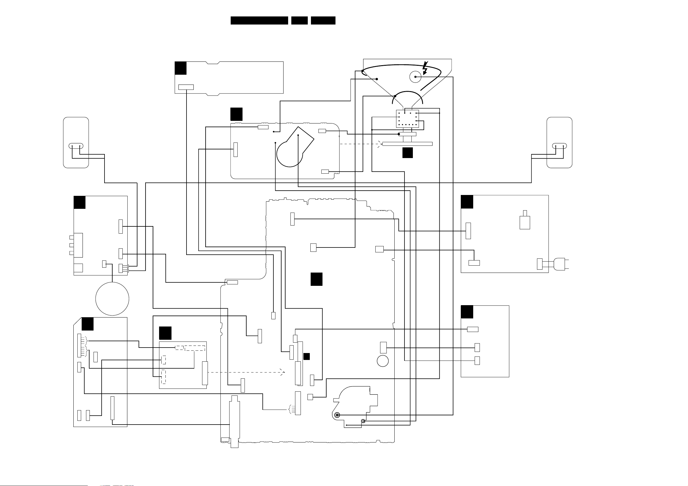
Wiring Diagram
TOP CONTROL PANEL
E
1010
3P
(component view)
CRT PANEL
B
RIGHT
SPEAKER
RED
BLACK
7P
5P
1351
1332
1352
CRT
SOCKET
19L04E AC 6.
1361
3P
1381
3P
AQUADAG
DEGAUSSING COIL
CRT
16:9
ROTATION
BLUE
RED
CRT PANEL
FRAME
COIL
B
YELLOW
ORANGE
SCAVEM
COIL
EHT
CRT
BLACK
RED
LEFT
SPEAKER
CVBS (YELLOW)
LEFT (WHITE)
RIGHT (RED)
HEADPHONE
SIDE
D
A/V PANEL +
HEADPHONE
PIP
F
91
9P
1212
NC
1220
4P
1219
NC
4P
4P
1214
1206
1279
3P
SUB
WOOFER
(OPTIONAL)
5P
to
TUNER
1252
1254
1278
FRONT INTERFACE
1693
6P
7P
1504
2P
5P
4P
MONO
A
3P
LTI/
H
CTI
1401
12P
5P
1451
2P
9P91
CARRIER
LOT
(track view)
LTI/CTI
H
INTERFACE
1216
1215
1206
7P 4P
4P 5P 15
1214
1212
12P
5P
1280
1207
TUNER
1682
3P
1206
7P
7P
1221
1204
7P
1212
1219
1505
2P
1404
2P
5401
J
1693
6P
1212
2P
LINEARITY&
G
PANORAMA
1462
3P
1464
2P
1461
2P
MAINS
SWITCH
1211
MAINS
CORD
2P
1005
3P
COMPAIR
CONNECTOR
E_14480_080.eps
170504
Block Diagrams, Test Point Overviews, and Waveforms
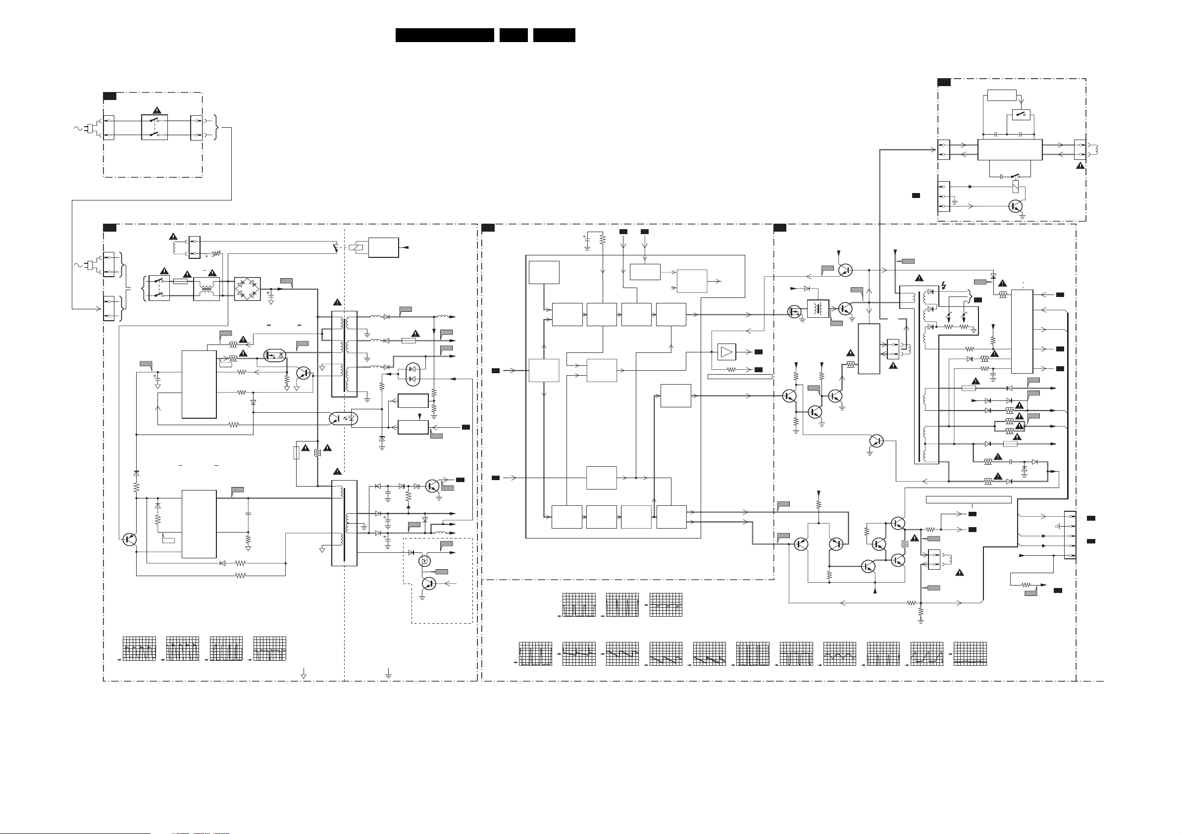
Block Diagram Supply and Deflection
SUPPLY AND DEFLECTION
SUPPLY
FRONT INTERFACE
J
1211
1
2
A1
1505
1505
F508 268V / div DC
1231
MAINS
SWITCH
(not USA)
POWER SUPPLY
Degaussing
1506
OR
MAINS
SWITCH
(not USA)
I511
6512
3519
7532
F511 15V5 / div DC
F531 2V7 / div DC
F537 0V (N.A.)
F552 130V / div DC
F561 15V9 / div DC
Coil
2511
6533
3530
I531
1212
1504
1500
T4E
7511
TEA1506T
2
Vcc
CONTROL
6
CTRL
STANDBY
SUPPLY
7531
TEA1620
3
Vcc
CONTROL
6
REG
11
AUX
F564 9V4 / div DC
F573 0V (N.A.)
1
2
5500 :
5502
DRAIN
IC
IC
SOURCE
DRIVER
SENSE
DEMAG
DRAIN
3507
t
6500
AC
I513
3513
14
3514
11
I519
3532
9
3517
7
3518
I533
14
12
6532
3534
3531
I513 I516 I519 I533
2534
3538
F508
2505
DC
MAIN
SUPPLY
3516
I516
D
S
7514
7512
G
6511
20L04E AC 6.
LINEARITY & PANORAMA
G
ONLY FOR:
28"WSRF LA/NA
32" WSRF LA/NA
28" WS-SF LA
1464
4
1
1462
TO 1221
A5
CONNECTIONS
1
2
3
DEFLECTION
HERCULES
Vbatt
-Vaudio
+Vaudio
+6VA
A4
A4
+3V
+6VA
+6VA
+6V
Vaux
2x
A4
INTF_Y GREEN_IN
A5
EHTinfo
A2
F401 130V / div DC
F402 32V8 / div DC
56
97
7200-H
(SYNC)
VIDEO
IDENT
MAIN
SYNC
SEPARATOR
EHTo
2240
PHI 1
DETECTOR
VERTICAL
SEPARATOR
HORIZONTAL
GENERATOR
PROTECTION
SYNC
F412 F414
2V / div DC
20µs / div
7541
1503
43
2
5520
9
8
4
5
3
2
4
3
35321532
1A
5531
4
5
1
2
(optional)
5551 5552
17
18
5562
13
14
5561
10
11
1
7515
TCET1103
2
6564
6535
10
9
6536
8
6
ENERGIZING
CIRCUIT
1
6551
6563
6562
3571
6573
F552
1543
7571
REFERENCE
7573
6565 6566
2564
2535
2536
V_DG
6571
CIRCUIT
+3V3
STANDBY
CIRCUIT
3565
F536
6537
G
7561
6676
DS
7536
F563
F561
3575
3576
Stdby_Con
I573
POWER-DOWN
F564
5537
F537
7535
I548
For IDTV only
F455 F458 F459
3232
112
OSC.
SAND-
CASTLE
X-RAY
VERTICAL
DIVIDER
A2 A2
EHTinfo
113 116
DETECTOR
VERTICAL
200V / div DC
20µs / div
VERTICAL
GUARD
DETECTOR
PHI 2
SAW-
THOOTH
Vguard
R.G.B.
BLANKING
HORIZONTAL
OUTPUT
E/W
+
GEOMETRY
VERTICAL
OUTPUT
+
GEOMETRY
F418
F452 -13V4 / div DC
F453 190V8 / div DC
5V / div DC
20µs / div
F460 F461
TO RGB
PROC.
7207
3291
HDRIVE
HD
SANDCASTLE
HD_PIP
EW_DRIVE
VDRA
VDRB
62
63
SEE BLOCK DIAGRAM VIDEO
108
106
107
I416 I417 I468I423 I433 I462
A5
A5
LINE + FRAME DEFLECTION
A2
LINE
F412
HD
6486
-9V
5402
7404
E/W
+8V
+8V
3420 3440
7410
I417
7484
3498
FRAME
+9V
F460
F461
3462
7455 7456
+6VA
BU4508DX
F418
7406
3463
7408
7405
3497
F414
LINE
OUTPUT
CIRCUIT
+
E/W
CORR.
7452
3465
-12V
7411
7454
1404
1
2
Vbatt
OR
7451
7453
F402
5445
3
1
HOR.
DEFL.
COIL
3466
3461
EHT
FOCUS
10
6
5
7
8
9
SEE BLOCK DIAGRAM VIDEO
VD
3474
Vguard
F458
1491
1
2
VER.
DEFL.
COIL
F459
FRAME_FB
3471
VG2
1454
+9V
I2SD/1
3442
6481
CRT
Vbatt
A5
A4
7460
ACTIVATING
I433
TO
B1
+Vbatt
3481
3410
6483 6484
6453
6456
3457
3455
CIRCUIT
7462
2466
LINEARITY AND
PANORAMA
CORRECTION
2474
2475
7463
6401
7401 : 7403
7480 : 7483
3411
3451
2403
6452
3458
3484
3485
1452
2456
6459
Vbatt
2464
2467
1463
EHTb
+
EHTinfo
+
BCL
PROC.
VIDEO/SUPPLY
3401
F401
POWER-DOWN
FRAME_FB
EHTb
EHTinfo
BCL
F452
F453
VIDEO/SUPPLY
F455
FILAMENT
6454
6455
EHTb
FILAMENT
VT_SUPPLY
1461
4
1
HOR.
DEFL.
COIL
A1
A4
A4
-12V
+9V
1401
TO 1351
5
B1
4
CRT
or
3
TO 1401
B3
2
CRT
INTERFACE
1
PAN E L
A4
100V / div DC
5µs / div
100V / div DC
5µs / div
2V / div DC
5µs / div
100V / div DC
5µs / div
HOT GROUND COLD GROUND
5V / div DC
20µs / div
20 V / div DC
5ms / div
1V / div DC
5ms / div
500mV / div DC
5ms / div
500mV / div DC
5ms / div
20V / div DC
20µs / div
500mV / div DC
20µs / div
10V / div DC
20µs / div
10V / div DC
20µs / div
10V / div DC
5ms / div
5V / div DC
5ms / div
E_14480_081.eps
140904
Block Diagrams, Test Point Overviews, and Waveforms
Testpoint Overview Mono Carrier
F001 A8
F002 A7
F003 A7
F004 A7
F005 A8
F006 A6
F007 A8
F008 A8
F009 B4
F010 A7
F011 A8
F200 B4
F201 C5
F202 B5
F203 B5
F204 C5
F205 C5
F206 C6
F207 B5
F208 B6
F209 A5
F210 A4
F211 A4
F212 A5
F213 A5
F214 B5
F215 B6
SERVICE
TESTPOINT
F216 C6
F217 C6
F218 C6
F219 B7
F220 B7
F221 B7
F222 C7
F223 B7
F224 C6
F225 C6
F226 B6
F227 A4
F228 C5
F229 C5
F230 B5
F232 B5
F233 B5
F237 B5
3139 123 5676.1
F238 B4
F239 B5
F240 C5
F241 C6
F242 B6
F243 C6
F244 B5
F245 C6
F247 A6
F248 A6
F249 A7
F250 C6
F251 B5
F270 B5
F401 C4
F402 D6
F404 D6
F407 D6
F412 C6
F414 E7
F415 E6
F416 E6
F417 E5
F418 D6
F419 D6
F420 D7
F451 C8
F452 C7
F453 D7
F454 C7
F455 D7
F456 E7
F457 E7
F458 C7
F459 C7
F460 C7
F461 C7
F462 E7
F463 D8
F464 E5
F465 E5
F466 E8
F500 C2
F501 D2
F502 D2
F503 E2
F504 E2
F505 E2
F506 E2
F507 E2
F508 E3
F509 E4
F510 D5
F535 C4
F536 C5
F537 C3
F541 C3
F542 C3
F551 C5
F552 D5
F561 C4
F562 D4
F563 C4
F564 C5
F573 C5
F581 B3
F582 B4
F583 C4
F682 B1
F683 B1
F685 B1
F691 C1
21L04E AC 6.
F692 D1
F693 E1
F694 C1
F695 C1
F696 D1
F697 E1
F698 C1
F699 D1
F701 C8
F702 C8
F703 C8
F704 C8
F705 B8
F706 C8
F707 B8
F708 B8
F709 B8
F710 B8
F711 C8
F712 B8
F713 B8
F714 B8
F715 B7
F716 A8
F717 A8
F718 A8
F719 B8
F731 C8
F732 C8
F733 C8
F734 C8
F735 B8
F736 B7
F737 B8
F738 B7
F739 B8
F751 A7
F752 A7
F901 B3
F903 B2
F904 B1
F905 B2
F910 B3
F911 B3
F950 B3
F951 B3
F952 A3
F953 A3
F955 A3
I001 A8
I002 A8
I003 A7
I004 A7
I005 A5
I006 A5
I007 A7
I008 A5
I009 A5
I010 A5
I011 A7
I012 A7
I013 A6
I014 A8
I015 A8
I016 A7
I017 B5
I201 A5
I203 A5
I204 A5
I205 A5
I206 A5
I207 B6
I208 C5
I209 B6
I210 B6
I211 B6
I212 B6
I213 A5
I214 A5
I215 A6
I216 B6
I217 B7
I218 B6
I219 B6
I222 B5
I223 B5
I224 B4
I225 B5
I226 B6
I227 A5
I228 B5
I229 C5
I230 B5
I231 B5
I232 A7
I233 B7
I234 A4
I235 B5
I236 B5
I240 A4
I241 A4
I401 E7
I402 E6
I403 E7
I404 E7
I405 E7
I406 E7
I407 E8
I409 E8
I410 E6
I412 E6
I413 C6
I414 D6
I415 C6
I416 C5
I417 D5
I418 D6
E_14480_095.eps
270504
I419 C6
I421 D7
I422 D7
I423 D5
I424 E8
I425 C6
I426 D7
I427 D5
I428 D6
I429 E8
I430 E6
I431 C7
I432 D6
I433 E6
I434 C5
I443 E7
I444 E7
I445 E7
I446 C5
I448 E7
I449 D8
I451 D7
I452 E8
I453 D7
I455 D7
I456 D8
I457 D7
I458 D7
I459 D7
I460 C8
I461 C8
I462 C8
I463 D8
I464 C8
I465 E7
I466 D7
I467 E8
I468 D7
I469 E8
I470 D8
I471 C8
I472 C7
I473 E5
I474 E6
I475 D8
I501 E3
I502 E3
I503 E2
I504 E2
I505 D1
I506 E3
I507 D3
I511 E5
I513 E5
I514 D4
I515 E4
I516 E4
I517 E4
I518 E5
I519 E5
I520 E5
I521 E4
I523 E5
I524 E5
I527 E5
I529 D3
I531 D3
I532 D3
I533 D3
I535 D3
I536 D3
I537 C4
I538 C3
I539 D3
I540 D4
I541 D4
I542 C3
I543 C2
I544 D3
I545 C3
I546 C3
I547 C3
I548 C3
I551 D5
I552 D5
I553 D3
I554 D4
I555 D4
I556 D4
I557 D3
I561 D4
I562 D4
I565 C4
I571 D5
I572 C5
I573 D5
I574 D5
I575 D5
I576 D5
I577 D5
I578 D5
I579 D4
I582 B4
I583 B4
I584 B4
I585 B4
I587 C4
I588 B4
I681 E1
I682 B1
I683 B1
I686 C1
I687 D1
I688 C1
I689 D1
I691 E1
I693 D1
I701 C7
I702 C8
I704 C8
I705 B8
I707 C8
I709 B7
I710 B7
I711 B8
I713 A7
I714 B7
I715 C7
I716 C8
I717 C7
I718 C7
I719 B7
I720 A7
I721 B8
I722 B7
I727 A7
I728 B7
I729 C7
I730 C7
I731 C7
I732 B7
I733 B7
I734 C7
I735 B7
I736 B7
I739 B7
I909 B3
I910 C3
I911 C3
I913 C3
I914 C2
I915 C3
I916 C2
I918 C3
I919 C2
I920 B3
I921 C2
I922 C2
I924 B3
I925 B3
I926 B2
I927 C2
I928 B1
I930 C2
I934 B2
I935 B1
I936 B2
I937 C2
I938 B2
I939 B2
I940 B2
I941 B2
I942 C3
I943 B2
I944 C3
I945 C2
I946 B3
I948 B3
I951 B3
I952 A3
I953 A3
I954 A3
I955 B3
I956 A3
I957 A3
I958 B4
I959 B4

Block Diagrams, Test Point Overviews, and Waveforms
Block Diagram Video
VIDEO
TUNER IF
A4
+5VS
+5V
A4
A4
A4
SDA
SCL
SEL-LLPIM
9002
50019003
1000
3001
3000
ERR
TV
I002
I001
FM
6 7
FM-RADIO
10
TV TUNER
5
7001
SELECTION
TUNER
+
4
FILTER
A2
98
VT
AGC
VT_SUPPLY
FM
IF
1
6001
BZX79-C33
F002
10
F004
11
PIP
PIP TUNER IF MULTISTANDARD VIDEO DEMODULATION
F2
+5VA
1000
UV1316/A
TV
3002 3001
7003
1002
1003
1004
ERR
4
79
PIP
+
TV TUNER
5
4
SDA
SDL
SSIF
VIF_1
VIF_2
RF_AGC
SIF1
SIF2
5001
VST
AGC
1002
1003
F002
11
IF
1
7001
SSIF
HERCULES
A4
7200-A (IF)
105
104
98
TUNER IF
100
AUDIO IF
99
QSS/AM
VIF_1
VIF_2
TUNER_AGC
SEL_P_N
TO
SEE BLOCK DIAGRAM AUDIO
AUDIO
PART
PHASE
DISC
VIDEO
IF
AGC
VCO
VIDEO
DEMOD
7201
TDA9887
1
2
14
3
PLL
1201
15 19
VIDEO
VIDEO
AGC
PLL
IF
DEM.
910
11
3207
AGC
ADJ.
3206
SOUND
TRAP
PLL
FM/QSS
SOUND
MIXER
AM
SOUND
DET.
22L04E AC 6.
CONN.
A5
1212
F216
INTF_Y/GREEN_IN
4
INTF_Pb/BLUE_IN
6
INTF_Pr/RED_IN
8
F217
F218
SEE BLOCK DIAGRAM
DEFLECTION
INTF_FBL
9
SANDCASTLE
10
SEE BLOCK DIAGRAM
1206
1
3
6
SEE BLOCK DIAGRAM CONTROL
DEFLECTION
E
D
INTF_BBL
DAC
DINT
A4
A4
A4
Y
Pr
Pb
SC1_FBL
H
1214
1216
LTI/CTI
1
3
5
1
7200-C
INSSW352
INTF_Y_OUT
INTF_Y
INTF_U_OUT
INTF_Pb
INTF_V_OUT
INTF_Pr
INTF_FBL
INTF_Y_OUT
INTF_U_OUT
INTF_V_OUT
(RGB/YPrPb/YUV
INPUT SWITCHING)
Yint
Uint
Vint
SELECTION
LOGIC
2
6
3
7
4
8
15
14
7611
TDA8601T
CLAMP
CLAMP
CLAMP
CLAMP
CLAMP
CLAMP
YUV
RGB
DVD
1212
1
2
3
SC1_RED_IN
SC1_GREEN_IN
SC1_BLUE_IN
49
50
51
YPrPb2/
YPrPb3
SELECTION
DVD
TO
DVD
DVD
3-STATE
3-STATE
3-STATE
3-STATE
A5
1212
1
2
3
12
11
10
13
165
F224
F225
F226
RGB2/
RGB3
SELECTION
RGB
DVD
7610
TDA9178T
7630
7635
6
YIN
LTI/C+I
8
UIN
PROC.
9
VIN
NC
PULSE FORMER
INTF_V-OUT
53
TO
RGB
19
YOUT
17
UOUT
16
VOUT
ERR
15
SC
1
1
SDA
SCL
3
INTF_Y_OUT
INTF_U-OUT58INTF_Pb/BLUE_IN
DVD
INTF_Y/GREE_IN
55
54
TO
YUV
57
YUV
TO
DVD
Y_2
Pb_2
Pr_2
INTF_FBL
SANDCASTLE
SDA
SCL
INTF_BBL
INTF_Pr/RED_IN
59
YUV
1212
4
6
8
9
10
12061215
1
3
6
DIGITAL SIGNAL PROC.
- 4:3 LINEAR/NON-LINEAR SCALING
- DOUBLE WINDOW PROC.
ADC
PIP-PROC.
F1
7202
17
ERR
16
SDA
SCL
SC1_CVBS_OUT
86
SWITCH
TO
AUDIO
PART
AM
See block
diagram
AUDIO
CVBS1_PIP
1219
INTF_CVBS_IN
1
INTF_CVBS_OUT
4
VD
2
HD_PIP
3
CONN.
A5
1219
INTF_CVBS_IN (NC)
5
INTF_CVBS_OUT
9
VD
7
HD-PIP
8
SW_SC2_CVBS
SC1_CVBS_IN
SC2_Y/CVBS_IN
SIDE_Y/CVBS_IN
CVBS1
SC2_CHROMA_IN
SIDE_CHROMA_IN
81
74
71
78
70
77
7242
SDA9488X
28
INPUT
24
26
4
3
SEE BLOCK DIAGRAM DEFLECTION
7200-B (CVBS I/O + FILTERS + COLOUR DECODING)
SWITCH
SYNC.
PROC.
ADC
STANDARD
DECODING
ERR
12
1
1241
2
MULTI
Y
UV
INPUT
SWITCH
VIDEO
IDENT
RGB
MATRIX
R
G
B
CVBS/Y
C
DAC
NC
FILTER
&TRAP
SWITCH
COMB
1220
R
G
B
1
2
3
FAST
RGB
SWITCH
11 12 13 6 5
CHROMA/CVBS
18
INTF_Y/GREEN_OUT
17
16
INTF_PbBLUE_OUT
15
OUTPUT
SWITCH
PAL, NTSC
SECAM
DECODER
INTF_PrRED_OUT
INTF_FBL
3244
SDA
3243
SCL
65
INTF_CVBS_OUT
YintYint
Uint
Vint
1212
1214
5
1
3
6
1
3
SC1_R/G/B
SC1_FBL
REAR I/O SCART (VIDEO PART)
A8
SC1-RED-IN
SC1-GREEN-IN
SC1-BLUE-IN
SC2-CVBS-OUT
SC2-CHROMA-IN
SIDE AV
D
32
SVHS
154
VIDEO
IN
A5
7606
7607
SW_SC2_CVBS
SW_SC2_CVBS
F201 2V / div DC
F203 2V / div DC
HERCULES
A4
7200-D (YUV PROCESSING)
Y
Pr
PEAKING
Pb
SCAVEM
PROC.
F205
500mV
10ms / div
/ div DC
WHITE/BLACK
STRETCH
GAMMA COR.
TINT CONTROL
SKINTONE
F206
1V / div DC
20µs / div
F240 F241 F242
500mV / div DC
20µs / div
500mV / div DC
20µs / div
500mV / div DC
MATRIXSATURATION
RGB
ADDER
R_Y
G_Y
B_Y
R
G
B
64
F331 F332 F333
20µs / div
500mV / div DC
20µs / div
500mV / div DC
FROM µP PART
R_OSD
G_OSD
B_OSD
OSD
INSERTION
CLAMP
MUTE
BLUE
STRETCH
+
&
CONTRAST
7200-E (RGB PROCESSING + CATHODE CALIBRATION)
20µs / div
FBL
BRIGHTNESS
+
PEAK WHITE
LIM.
BEAM
CURRENT
LIM.
500mV / div DC
20µs / div
CATHODE
CALIBRATION
46
3226
42
STAGE
3227
43
3228
44
45
OUTPUT
BCL
A2 A4
7308
BOUT
GOUT
ROUT
IBLACK
SVM
A5
CRT
B1
F240
F241
F242
ROT
13311204
B
1
1
2
3
4
5
6
7
G
2
R
3
4
5
6
7
+200V
+200VA
BC_INFO
SVM
ROT
2351
3351
1351
SCAVEM
B2
ROT
SVM
F331
7330
3
F332
1
2
F333
VSVM
FILAMENT
1351
123 45
to 1401
A2
DEFLECTION
FILAMENT
1381
1
ROTATION
OUTPUT
FILAMENT
VSVM
SCAVEM
OUTPUT
+200VA
F341
3332
7
B
3334
9
G
3336
8
R
5
5352
EHT-b
1332
11
F338
F339
B
6
G
8
R
10 9 5 7 1
ROTATION
COIL
2
(OPTIONAL)
1361
1
SCAVEM
COIL
2
(OPTIONAL)
AQUADAG
DEFLECTION
FOCUS
VG2
A2
FROM DEFLECTION
E_14480_085.eps
280504
CRT
25kV
EHT
7701
SCART 1
21
20
19
16
15
SC1-CVBS-OUT
SC1-CVBS-IN
SC1-FBL
11
7
SCART 2
21
20
19
16
15
8
SC1-STATUS
SC1-R/G/B
SC2-CVBS-OUT
SC2-Y/CVBS-IN
A4
11
CONNECTION
7
6
5
SC2-STATUS/ITV_MSG
SC2-CHROMA-IN
SIDE_CHROMA_IN
SIDE_Y/CVBS_IN
A4
8
7
A5
1207
1252
Y
7
6
C
5
Block Diagrams, Test Point Overviews, and Waveforms
Testpoint Overview CRT, LTI & PIP Panel
CRT
3139 123 5889.1
23L04E AC 6.
F331 A1
F332 A1
F333 A1
F334 A1
F335 A1
F336 A1
F338 A1
F339 A2
F340 A2
F341 A2
F351 A1
F352 A1
F353 A1
F354 A1
F356 A2
F360 A1
F361 A3
F362 A3
F363 A3
F381 A3
F382 A3
I330 A1
I331 A1
I332 A1
I333 A1
I334 A1
I335 A1
I336 A2
I337 A1
I351 A1
I353 A2
I355 A2
I357 A1
I360 A1
I361 A2
I362 A2
I364 A3
I366 A3
I368 A3
I369 A3
I371 A3
I372 A3
I381 A2
I383 A2
I385 A2
I386 A2
I387 A3
I388 A2
I389 A2
I390 A2
I391 A2
I392 A1
1610 A2
1611 A2
1612 A1
1613 A2
1614 A1
1616 A1
1617 A2
1618 A1
1619 A2
1620 A1
1621 A2
1622 A1
LTI INTERFACE
3139 123 5740.1
1623 A1
1624 A2
1626 A2
1627 A1
1628 A1
1633 A2
PIP
3139 123 5821.1
E_14480_091.eps
020404
F001 B5
F002 B4
F003 C4
F201 B4
F202 A5
F240 C3
F241 A3
F242 A3
F243 A3
F244 A3
F245 B4
F271 A3
F272 A2
F273 A2
F274 B2
F275 A3
F276 B2
F279 B3
F501 A1
F502 A2
F503 A5
F504 A5
F505 B2
F506 C2
F507 C1
F508 C2
I001 B5
I002 C4
I003 C4
I004 C4
I005 B4
I006 B4
I007 C4
I201 B5
I202 A4
I203 A4
I204 A4
I205 B5
I206 B5
I207 A5
I208 A4
I209 A4
I210 B5
I213 A5
I217 A4
I241 C2
I242 B3
I243 B2
I244 C3
I245 C3
I248 B3
I249 A4
I250 A4
I251 A3
I252 A3
I253 B3
I254 B3
I255 B3
I256 B4
I257 C3
I258 B3
I259 B3
I263 B2
I271 A3
I273 A3
I274 B2
I276 A2
I277 B2
I278 B2
I279 A2
I280 B2
I281 C2
I501 A1
I502 A1
I503 A1
I504 B1
I505 B1
I506 B1
I507 B1
I508 B1
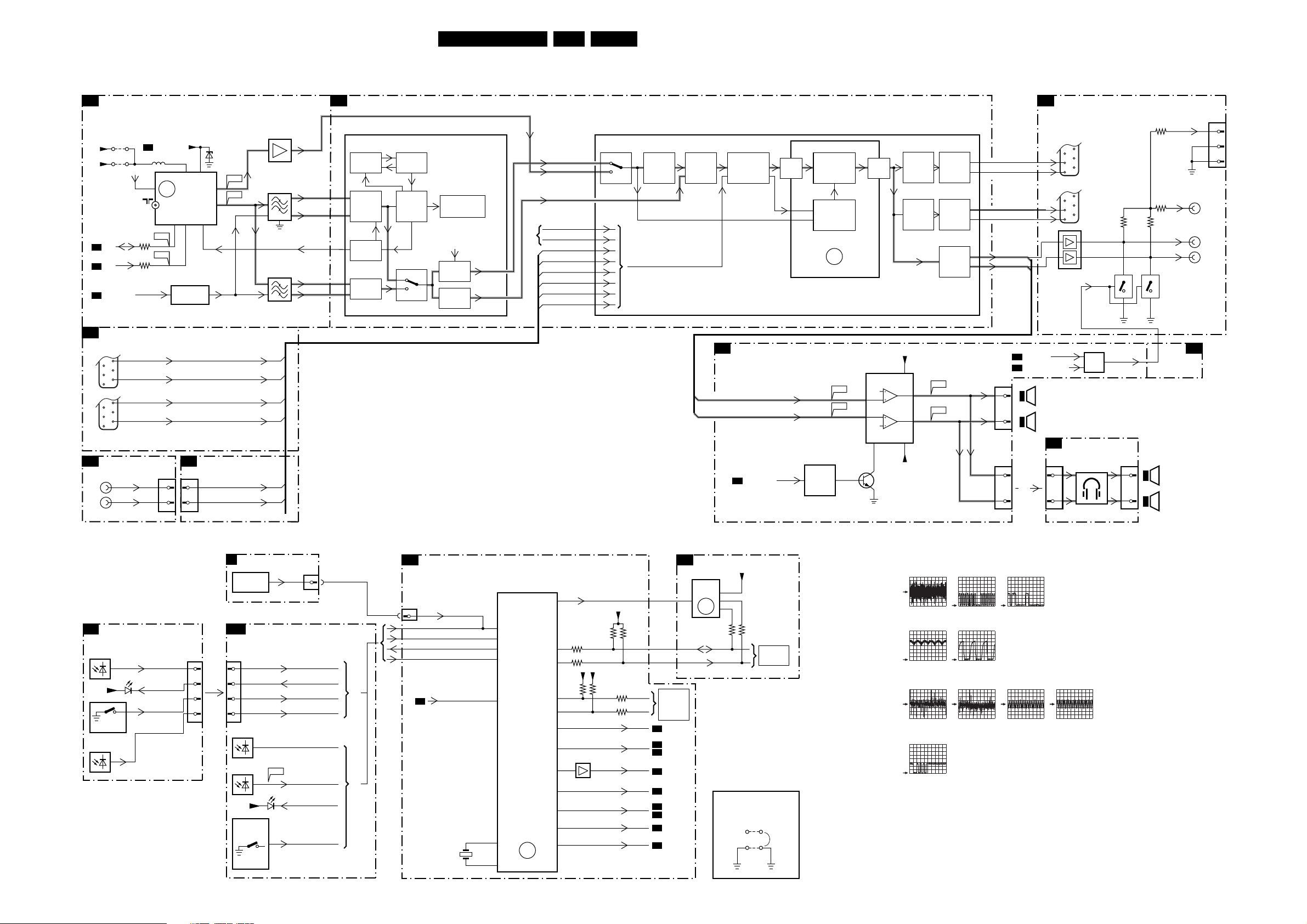
Block Diagrams, Test Point Overviews, and Waveforms
Block Diagram Audio/Control
AUDIO
TUNER IF
A3
+5V
+5VS
SDA
A4
SCL
A4
SEL-LLPIM
A4
REAR I/O SCART
A8
SCART 1
SCART 2
SIDE AV
D
L
R
9002
6
3
2
1
6
3
2
1
FM
3001
3000
VT_SUPPLY
A2
50019003
1000 6, 7 9
2
ERR
10
TV
I002
I001
1252
3
1
FM-RADIO
TUNER
+
TV TUNER
5
4
7001
FILTER
SELECTION
A5
1207
3
1
6001
BZX79-C33
VT
F002
10
FM
F004
11
IF
AGC
1
CONNECTIVITIES
SIDE_L_IN
SIDE_R_IN
SC1_L_IN
SC1_R_IN
SC2_L_IN
SC2_R_IN
7003
1002
1003
1004
SSIF
VIF_1
VIF_2
RF
SIF1
SIF2
A4
24
25
31
29
30
HERCULES
7200-A (IF)
PHASE
DISC
VIDEO
IF
TUNER IF
AGC
AUDIO IF
QSS/AM
VCO
VIDEO
DEMOD
PLL
To VIDEO PART
see block diagram
VIDEO
PLL
SOUND
MIXER
AM
SOUND
DET.
FM/QSS
AM
N.C.
FM/QSS
SSIF
AM
INTF_R_IN 75
INTF_L_IN 76
SC2_R_IN 72
SC2_L_IN 73
SIDE_R_IN 79
SIDE_L_IN 80
SC1_R_IN 94
SC1_L_IN 95
24L04E AC 6.
7200-F (AUDIO)
96
FM
DEM.
AMPLI
+
MUTE
MAIN_OUTL
MAIN_OUTR
AUDIO
SOURCE
SELECTION
AUDIO AMPLIFIER
A7
A4
VOL_MUTE
DIGITAL PART
ADC DAC
DIGITAL
PROCESSING
DIGITAL
STEREO
DECODER
7991
7992
VOLUME
+
MUTE
SOUND
SOUND
ERR
19
I951
I952
7990
TDA2616Q
1
9
2
7991
AUDIO
SELECT
AUDIO
SELECT
V AUDIO+1
7
5
-V AUDIO
REAR I/O SCART
A8
3762
SCART 1
SC1_L_OUT
SCART
CINCH
OUTPUT
OUTPUT
OUTPUT
F952
4
F955
6
93
SC1_R_OUT
92
SC2_L_OUT
67
HP
LS
66
68
69
SC2_R_OUT
MAIN_OUTR
MAIN_OUTL
A4
A4
1281
5
2
1280
1
2
Stby_Con
POWER_DOWN
OR
6
3
2
1
SCART 2
6
3
2
1
7705
5
2
L 8 Ohm/15W
R 8 Ohm/15W
SIDE AV
D
5
2
4
1
MUTING
7993, 7994
MUTE
3764 3761
7703 7702
MUTING
12781254
1
2
3757
L 8 Ohm/15W
R 8 Ohm/15W
SPDIF
(optional)
1228
SUBWOOFER
(optional)
MONITOR
OUT
L
R
A5
1
2
3
CONTROL
FRONT INTERFACE
J1
(PARTLY)
6692
TSOP1836
+3.3V
ON/OFF
USA only
6693
6691
KEYBOARD
LIGHT_SENSOR
LED
TOP CONTROL
E
LOCAL
KEYBOARD
FRONT CONTROL
A9
1693
3
IR
4
5
6
1693
3
4
5
6
6693
6692
TSOP1836
+3.3V
LOCAL
KEYBOARD
(USA only)
+
ON/OFF
F692
6691
1010
2
LED
KEYBOARD
LIGHT_SENSOR
LIGHT_SENSOR
LED
KEYBOARD
IR
OR
IR1
OR
HERCULES (CONTROL)
A4
1682
2
KEY_PROTN 9
IR 32
LED 30
LIGHT-SENSOR 14
POWER_DOWN 31
A1
1205
24MHz
7200-G (Control)
TDA12001H1
I/O PORTS
IIC BUS
TRANSCEIVER
PWM
OUTPUTS
TELETEXT
(close caption)
119
118
+
+
+
CPU
+
+
ROM
RAM
ERR
20
22
3207
20
3214
21
2
1
18
15
7205
17
16
23
24
25
SEL_SC2_INTF
WRITE_PROTECT
+3.3V
32803279
VOL_MUTE
Stdby_Con
SEL_LLPIM
I2SD/1
Reset__5V
ROT
+3.3V
3266
3265
FEATURES
A5
EEPROM
(NVM)
7
ERR
32043202
SDA
SCL
see
E
IIC
DIAGRAM
D
(FOR LTI
AND PIP)
A7
A1
A7
B2
+3.3V
8
6
5
9
36043605
see
IIC
DIAGRAM
F003 0V (N.A.)
F201 2V / div DC
F203 2V / div DC
F004
200mV
10ms
F205
500mV
10ms
50mV
2ms
F692
2V
2ms
/ div AC
/ div
/ div DC
/ div
/ div AC
/ div
/ div DC
/ div
I001 I002
1V
/ div DC
20µs
/ div
F206
1V
/ div DC
20µs
/ div
I952I951 F952 F955
50mV
/ div AC
2ms
/ div
1V
20µs
500mV
/ div DC
/ div AC
2ms
/ div
/ div
500mV
2ms
/ div AC
/ div
A3
A5
G
A5
A5
SERVICE JUMPER
9275
SDM
9252
E_14480_087.eps
280504

Block Diagrams, Test Point Overviews, and Waveforms
I2C and Supply Voltage Overview
SUPPLY LINES DIAGRAM
POWER SUPPLY
A1
SUPPLY
PRIMARY
SIDE
5520
9
8
4
5
3
2
3
4
3532
5531
4
5
1
2
HOT GROUND COLD GROUND
7541
1503
43
ENERGIZING
2
CIRCUIT
1
(optional)
5551 5552
17
18
5562
14
13
5561
10
12
1
7515
TCET1103
2
6564
6535
10
6536
8
6537
6
6551
6563
6562
3571
6573
2564
2535 6676
2536
1543
7571
REFERENCE
7573
STANDBY
6565 6566
V_DG V_DG
6571
3575
CIRCUIT
CIRCUIT
3576
+3V3
STDBY_CON
POWER-DOWN
7561
3565
5537
D
S
7535
G
7536
only used in sets with DVD
Vbatt
-Vaudio -Vaudio
+Vaudio
+6VA
AUDIO_AMPLIFIER
A7
Vaudio+1
CLASS D
A6
AUDIO AMP
(RESERVED)
+Vaudio
A4
A4
+6VA
+3V
+6VA
+6V
Vaux
2X
2X
2X
1903
see diversity table
*
+6VA
HERCULES
A4
+3V
+3.3V
Stdby_Con
A1
POWER_DOWN
A1
+5V
+Vbutter
+6V
+8V
9911
9910
25L04E AC 6.
LINE + FRAME DEFLECTION
A2
+Vbatt
FILAMENT
To 6403, 3480,
3420, b-7401,
c-7403
on
To
VERTICAL
DEFLECTION
7605
7604
3609
A2
Vbatt
1401
1
2
3
4
5
+3V (N.C.)
+6V
+6VS
+3.3V
+5V
5445
7990
TDA2616Q
5
OUTPUT
7
AUDIO
Vaudio+1
5402
A4
EW_DRIVE
7405
OUTPUT
CIRCUIT
CORR.
7404
HDRIVE
A4
To 6407
on
A2
3401
VT_SUPPLY
LINE
3
1
1404
1
2
+
E/W
HOR.
DEFL.
COIL
*
V_DG
7200
HERCULES
19
35
125
15
31
+3.3V
+5V
+Vbutter
+6V
+8V
PWM1
DECDIG
115
16
+6VA (To 3445)
6207
3217
3295
2204
7202
VT_SUPPLY
2X
3210
3211
3206
3209
3208
7210
G
7204
7201-2
7203
7201-1
7209
D
S
D
G
S
+3V
+1.8V_A
+1.8V_B
EHT
FOCUS VG2
10
6
5
7
8
9
BCL
1454
6453
6456
3457 2456
3455
TO
CRT
B1
6452
3458
3484
3485
1452
6459
+3V
+6V
VT_SUPPLY
RESET +5V
A4
Vbatt
6483 6484
To 3405, 3463,
3475
on
A2
VIDEO SUPPLY
6455
3606
6454
FILAMENT
4604
VIDEO SUPPLY
-12V
+9V
7603
L78L33ACZ
13
3608
3607
CRT
B1
1351
A5
+9V
VSVM
1
+200V
2
FILAMENT
3
4
5
FEATURES & CONNECTIVITIES
+9V
+3.3V
1X
2X
+5V
1X
4611
B2
FILAMENT
3639
3610 6610
9605
SCAVEM
VSVM
FILAMENT
+200V
3351
F1
1212
962
+200A
1221
1
+9V
1212
12
+9V
+9V
+9VA
+9VA_1
+8V
Vbuffer
PIP POWER SUPPLY
+9V
3505
7502
5501
+3V3
5502
7501
MC34063AD
SUPPLY
6502
IC
+8V
Vbuffer
6509
6503
-/B33
TUNER IF
A3
+5V
5001
+5V
VT_SUPPLY
REAR I/O CINCH
A8
Vbutter
FRONT CONTROL
A9
+5V
1X
1X
1X
5507
????
1693
1462
1212
12
6504
2507
PIP TUNER IF
F2
9002
6001
-/C33
3690 3693
6694
-/C5V1
FRONT INTERFACE
J
LINEARITY & PANORAMA
G
1
LTI/CTI
H
3610
6610
9V
5504
5506
5220
5010
9613
+5V
+3V3
+5VS
+5VA
+33V
To TUNER
Pin 6.7
To TUNER
Pin 9
Vbutter
To LED
To 3-6692
(IR_REC)
+6V
+9V
+8V
1693
1
1216
4
I2C BUS INTERCONNECTION DIAGRAM PIP MODULE
A4
HERCULES
7200
SET
PROCESSOR
PAR T OF
VIDEOPROCESSER
(HERCULES)
ERR
19,20
+3.3V
+3.3V
3202
20
21
22
+3.3V
3279 3280
2
1
3207
3214
62116210
+3.3V
3266
3265
3204
SDA
SCL
WRITE_PROTECT
E
D
A5
ERR
6
FEATURES & CONNECTIONS
+3.3V
3601
56
PCF8511
EEPROM
7
(NVM)
7601
ERR
9
TUNER IF
A3
1206 1206
E
D
36043605
30003001
54
1000
TUNER
ERR
10
COMPAIR
1005
1
2
3
For
only
1
3
LTI/CTI INTERFACE
H
1
3
14 11
7610
TDA9178T
LTI/CTI
PROC.
ERR
15
SDA
SCL
36173616
F1
1215 1214
1
3
PIP POWER SUPPLY TUNER IF
56
7242
SDA9488X
PIP
PROC.
ERR
12
SDA
SCL
32433244
1
3
F2A5
30013002
54
1000
UV1316
TUNER
PIP
ERR
4
10 11
7201
TDA9887
PIP
IF
DEMO.
ERR
16
32063207
ERROR CODE LIST
ERROR Device Error description Check item Diagram
0 Not applicable No Error
1 Not applicable X-Ray / over-voltage protection
2 Not applicable High beam (BCI) protection 3404, 7405 A2
3 Not applicable Vertical guard protection 3466, 7451, 7452, 7453,
4 Tuner UA1316/A I2C error while communicating
5 Not applicable +5v protection 7604, 7605 A5
6 I2C bus General I2C error 7200, 3207, 3214 A4
7 Not applicable - - 8 Not applicable - - 9 24C16 I2C error while communicating
10 Tuner = I2C error while
11 TDA6107/A Black current loop instability
12 SDA9488X I2C error while communicating
13 Not applicable - - 14 DVD Loader I2C error while communicating
15 TDA9178T/N1 I2C error while communicating
16 TDA9887 I2C error while communicating
17 Not applicable - - 18 Not applicable - - 19 TDA1200 I2C error while communicating
20 TDA1200 I2C error while communicating
(US only)
with 2nd tuner
with the EEPROM
communicating with the PLL
tuner
protection
with the PIP processor
with the DVD Interface module
with LTI module
with PIP_Demodulator
with SSD stereo sound
decoder
with video cosmic in Hercules
IC
2411, 2412, 2413, 6404,
6411, 6412.
7454
1000, 5010
(PIP Module)
A2
A2
F2
7601, 3604, 3605 A5
1000, 5001 A3
7330, 3351, CRT B1
7242 (PIP Module) F1
DVD Interface module DVD Loader
7610 H
7201 F2
7200 A4
7200 A4
E_14480_084.eps
060504
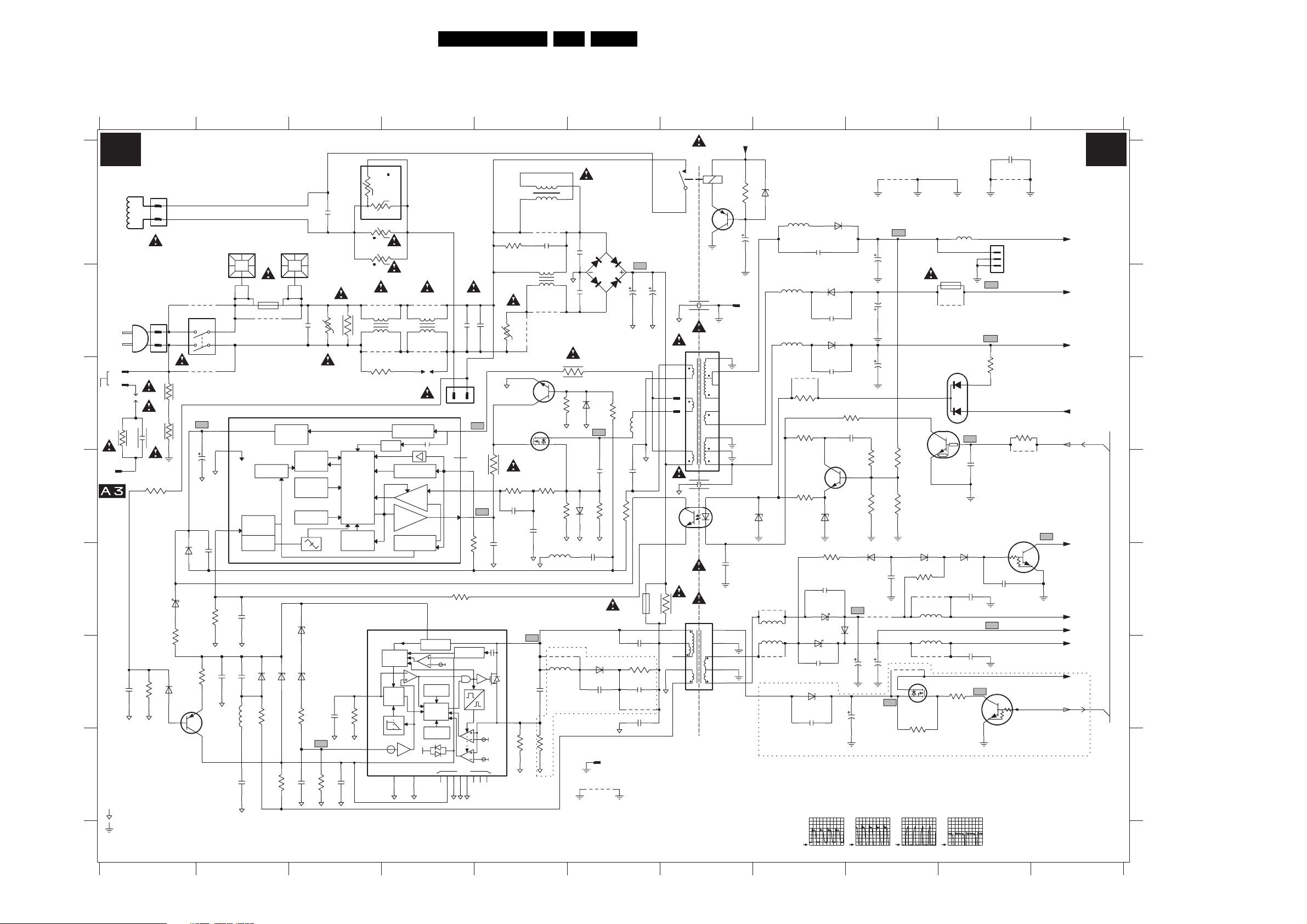
Circuit Diagrams and PWB Layouts
7. Circuit Diagrams and PWB Layouts
26L04E AC 7.
Mono Carrier: Power Supply
1 234567
14
16V4
Vaux_GND
2542
For Heatsink
5512
18
17
16
15
14
13
12
AUDIO_GND1
11
AUDIO_GND2
10
2570
470P
9V3
8V2
220n
2573
Vaux_GND
7
8
Vaux_GND
9
F552 130V / div DC
F561 15V9 / div DC
V_DG
47K
3541
6541
16V4
25V47u
2541
1542
6573
4534
For IDTV Only
F564 9V4 / div DC
F573 0V (N.A.)
POWER SUPPLY
A1 A1
DEGAUSSING COIL
1504
A
B
1508
1509
For
Lightning
Protection
C
3506
1510
TO 1013 OF
D
(For
Lightning
Protection)
E
F
"$"
G
..V.. Normal Operation
(..V..) Standy Mode
3M3
2528
**
FOR MAINS 120V AC 170V (177V)
HOT GROUND
COLD GROUND
2
1
1505
3500
3501
1n5
2509
3529
*
3528
6538
220V AC 309V (317V)
2
1
6512
3519
*
3V8
*
*
2
1
*
3M3
3M3
6511
BAT54 COL
15K
9507
1506
56
4
3
MAINS SWITCH
9508
I511
15V5
2511
22u 50V
2517
RGP10D
3512
3527
2532
*
13V
7532
BC857B
0V3
1501
PFC5000
7511
TEA1506T/N1
2
Vcc
3
Gnd
6
Ctrl
0V
1n0
1K2
2512
10u
2530
5533
2544
*
T4E.250V
for ITV only
FREQUENCY
CONTROL
INPUT
CONTROL
CIRCUIT
BURST
DETECTOR
100n
6532
330p
33u
3534
10n
1500
9500
BAV21WS
100R
1502
PFC5000
SUPPLY
MANAGEMENT
TEMPERATURE
PROTECTIOM
6533
6534
6531
BZX384-C15
3530
3531
2533
100K
470n
2500
VOLTAGE
CONTRLLED
OSCILLATOR
OVER
POWER-ON
RESET
BZX384-B6V8
220R BZX384-B3V9
I531
4n7
3537
2501
3XXX
*
2531
2K2
RES
3504
V
MAXIMUM
PROTECTION
470p
2549
LOGIC
CONTROL
CIRCUIT
ON-TIME
3533
100p
3
+t
Rs
3523
Rp
2
*
3507
+t
*
3509
+t
RES
9501
RES
5501
4
1
1M5
23
DMF-2405
9503
RES
3502
*
CURRENT SOURCE
VALLEY
*
TEA1620 (Basic)
7531
TEA1623 (IDTV)
LOGIC
STOP
5
RC
OSC
1V
LOW FREQ
8K2
F
1.8 U
2.5V
6
REG
2V7
+
11
AUX
0V3
GND SGND NC
4
1
9502
*
5500
1
*
23
9504
*
3503
*
DSP
START-UP
START-UP
CURRENT SOURCE
CURRENT
SENSING
OUTPUT
DRIVER
OVER
POWER
PROTECTION
3
SUPPLY
PWM
POWER-UP
10X
-
4
2
1507
For 70W Subwoofer
14
Drain
HVS
Demag
Sense
Driver
3518
3K3
VCC
VALLEY
+
THERMAL
SHTDWN
PROT
LOGIC
RESET
110
789
RES
2502
1
297V
7
0V
9
0V
11
2V2
3517
131415162
I513
2508
I519
BLANK
330K
SOURCE
+
+
100n
3514
2513
DRAIN
*
3510
470p
3508
470R
BC847B
3522
47K
2516
100n
-8V3
12
0V
*
*
23
14
DMF-2810
4R7
RES
9511
-T
7514
2V3
7512
*
2V3
G
2519
I533
68P
2534
3538
2R2 (IDTV)
1R8 (Basic)
5502
9506
2506
33n
5503
9505
RES
3515
1K0
100p
0V
3R3
3539
81
45
3513
2K2
0V
3524
295V
D
S
0R1
3XXX
5513
1u0
9532
5532
For IDTV Only
Vaux_GND
2503
2504
47K
6575
6514
2
2n2
6500
4
*
3
2n2
BAS316
I516
2514
*
3XXX
1N5062
2518
10n
6540
2546
470p
1545
Provision For
Lightning Protection
4538
1
3K3
3521
1n5
4K7
3511
For IDTV
Vaux_GND
2505
5511
2515
Only
2550
33P
2545
9512
2543
I508
*
1532
3542
68K
10n
2n2
2507
470p
T315MA
"$"
3532
F508 268V / div DC
1503
LKS1AF
23
7541
BC857B
Vaux_GND
RES
*
*
2
3
4
5
8
9
15V6
14
5V
32
7513
TCET1103(G)
4R7
5531
56
4
3
2
110
SS22220-03
COLD
HOT
F511 15V5 / div DC
F531 2V7 / div DC
F537 0V (N.A.)
3139 123 5676.5
8 9 10 11
2553
3
2
1
I563
I561
3572
A1
A2
10n
Vaux_GND
I536
I548
1535
0V
2566
100n
PDTC143ZT
180P
9509
Vaux_GND
for DVD
100R
7561
PDTC143ZT
BZX384-C12
BZX79-C9V1
RES
5534
1u0
5535
1u0
4535
RES
9510
Audio_Gnd
2551
6551
*
1n
6563
5551
5562
*
2565
1n
AUDIO_GND1
5561
6562
*
2561
9513
1n
RES
3571
*
3578
470R
7V6
6V2
3577
1K5
6572
3563
220R
2538
470P
6535
SB160
6536
SB180
2539
470P
6537
STPS10L60D
2540
1n
I513 I516 I519 I533
100V / div DC
5µs / div
3579
2K2
2571
15n
7571
BC547B
6V8
BZX384-B6V2
6576
2537
Vaux_GND
AUDIO_GND2
3573
3574
6564
BAS316
Vaux_GND
I565
BAS316
6.3V1m0
2535
Vaux_GND
2m2 16V
100V / div DC
5µs / div
AUDIO_GND2
I552
160V
2552
100u
2563
*
2562
**
7573
PDTC114ET
15K
3575
3576
*
100n
2564
4537
10V
4536
2536
2m2
I545
82K
4K7
6565
*
3565
*
7535
SI2307DS
3535
1K0
2V / div DC
5µs / div
9536
RES
5536
RES
5537
RES
9537
RES
AUDIO_GND1
*
*
K
8V2
5552
27u
1543
9514
6571
BAV70
6566
BAS316
3536
*
100V / div DC
5µs / div
I573
2572
2547
1u0
2548
1u0
Vaux_GND
Vaux_GND
3589
9589
7536
I564
3V3
Vaux_GND
POWER_DOWN
Vbatt
140V
-Vaudio
-16V
+Vaudio
+16V
+6VA
Stdby_Con
A4
+3V
+6VA
+6V
Vaux
B
A4
F_16120_001.eps
121205
G
A
B
C
D
E
F
1500 B2
1501 A2
1502 A3
1503 A7
1504 A1
1505 B1
1506 B1
1507 C4
1508 C1
1509 C1
1510 D1
1532 E6
1535 A10
1542 B7
1543 B10
1545 G6
2500 B3
2501 A3
2502 B4
2503 A6
2504 B6
2505 B6
2506 A5
2507 B6
2508 B5
2509 C1
2511 D2
2512 E2
2513 E5
2514 D6
2515 D6
2516 D5
2517 E2
2518 E6
2519 D5
2528 F1
2530 F2
2531 F3
2532 F2
2533 G3
2534 F5
2535 F9
2536 F9
2537 F9
2538 E8
2539 F8
2540 F8
2541 A7
2542 B7
2543 F6
2544 G2
2545 F6
2546 F6
2547 E10
2548 F10
2549 G3
2550 F6
2551 A8
2552 A9
2553 A10
2561 C8
2562 C9
2563 B9
2564 E9
2565 B8
2566 E10
2570 D7
2571 C9
2572 D10
2573 E7
3500 C1
3501 C1
3502 C3
3503 C4
3504 B3
3506 C1
3507 A3
3508 A5
3509 A3
3510 B5
3511 D6
3512 E2
3513 C6
3514 D5
3515 D5
3517 E4
3518 E4
3519 F1
3521 C6
3522 D5
3523 A3
3524 C5
3527 F2
3528 F1
3529 D1
3530 F3
3531 G2
3532 E6
3533 F3
3534 F2
3535 F9
3536 F10
3537 G3
3538 G5
3539 G5
3541 A7
3542 F6
3563 E8
3565 E9
3571 C8
3572 C10
3573 D9
3574 D9
3575 D9
3576 D9
3577 D8
3578 C8
3579 C9
3589 C10
3XXX B3
3XXX D5
3XXX D6
4534 E8
4535 F8
4536 F9
4537 E9
4538 G6
5500 B4
5501 B3
5502 A5
5503 B5
5511 C6
5512 B7
5513 E5
5531 E7
5532 F5
5533 F2
5534 E8
5535 F8
5536 E9
5537 F9
5551 A8
5552 A10
5561 B8
5562 B8
6500 A6
6511 E1
6512 E1
6514 C6
6531 F2
6532 F2
6533 E3
6534 F3
6535 E8
6536 F8
6537 F8
6538 F1
6540 F6
6541 A8
6551 A8
6562 B8
6563 B8
6564 E9
6565 E9
6566 E10
6571 C10
6572 D8
6573 D7
6575 D6
6576 E8
7511 C2
7512 C5
7513 E7
7514 C5
7531 E3
7532 F2
7535 F9
7536 F10
7541 A7
7561 D10
7571 D9
7573 C9
9500 B2
9501 B3
9502 B4
9503 B3
9504 B4
9505 B5
9506 A5
9507 B2
9508 C2
9509 A10
9510 A9
9511 B5
9512 F6
9513 C8
9514 B10
9532 F5
9536 E9
9537 F9
9589 D10
1 23456789
10 11

Circuit Diagrams and PWB Layouts
Mono Carrier: Diversity Table for A1
12345678910
27L04E AC 7.
DIVERSITY TABLE FOR
REGION
MAIN RANGE
A
B
C
D
SET
VBATT
AUDIO
OUTPUT
1508
1510
2505
2506
2508
2509
2528 --- --- --2542
2570
3505
3506
3507
3508
3514
3520
3527
3528
3529
3523
3565
3574
5500
5502
5512
6500
6538 --6551
6565
7512
7532 --- --9502
9504
9506
AUDIO
OUTPUT
1543
2562
25V 1000uF
2563
25V 1000uF 25V 2200uF 25V 2200uF
3571
3572
6562
6563
9514
27RF
27FSQ 32RF
130V 130V
2X5W
2X10W
--- ---
200V 470U 200V 470U 200V 470U 400V 330U
--- ---
--- --- ---
--- --- ---
250V 1N5 250V 1N5
--- --- ---
1MA/423V 1MA/423V 1MA/423V 1MA/612V 1MA/612V 1MA/612V
---
---
--- --- --- --- --- --- --- --100R 100R 100R 47R 47R 47R
0R18 0R18 0R18 0R33
---
---
---
145V 1R5
15K 15K 15K 18K
150K 150K
--- --- ---
--- --- --- --- --- --- --- ---
GBU4JL GBU6JL GBU6JL GBU4JL
STTH8L06D BYV29X-500
UDZS9.1B UDZS9.1B UDZS9.1B UDZS7.5B
FQPF9N50 FQPF9N50
JMP
JMP
JMP
2X5W 2X10W 2X10+20W 2X15W
---
220R 220R 680R
220R 220R 470R
SB360 SB360 SB380
SB360 SB360
JMP
SS40310-01SS40310-01 SS40312-01 SS42315-01 SS42315-01 SS42315-01
--- ---
--25V 2200uF
25V 2200uF
220R
220R
SB360
SB360
JMP
LR
26WSRF
30WSRF
32FSQ
143V 130V 130V 130V
2X5W
2X10W
---
144V 3R
---
---
---
---
--- ---
JMP
JMP
JMP
25V 2200uF 25V 2200uF
2X5W
2X10W
---------
---
---
250V 1N5 250V 1N 250V 1N 250V 1N
---
144V 3R
---
---
---
---
33K 150K 150K 150K
BYV29X-500 STTH8L06D STTH8L06D STTH8L06D STTH8L06D STTH8L06D BYV29X-500 STTH8L06D
FQPF9N50 FQPF7N80 STP10NK8OZFP STP10NK8OZFP
JMP
JMP
JMP
2A 250V 2A250V
--- ---
POWER SUPPLY
LATAM / APNAFTA
FR
21RF
2X10W 2X5W
WIRE SIN
180 SIN
18ST BK
WIRE SIN
400 SIN
18ST BK
---
275V 100N 275V 100N
250V 1N5 250V 1N5 250V 1N5 250V 1N5 250V 1N5
470N 470N 470N 470N 470N 470N 470N 470N
250V 470P
3M3
--- --- --- --- --- --- ---
47K
1M
2M2
276V 4R5 276V 4R5 276V4R5 276V 4R5 276V 4R5 276V 4R5 276V 4R5
10MH 2A 10MH 2A 10MH 2A 10MH 2A 10MH 2A
BAS316 BAS316 BAS316 BAS316 BAS316 BAS316 BAS316 BAS316 BAS316 BAS316 BAS316 BAS316 BAS316
---
--- --- --- ---
JMP
SB380
25RF
29FSQ 29RF 29RF 28WSSF
130V 143V 143V 130V 130V 130V 130V 130V
2X10W
WIRE SIN
180 SIN
18ST BK
WIRE SIN
400 SIN
18ST BK
400V 330U 400V 330U 400V 330U 400V 330U
--- --- --- ---
250V 470P 250V 470P 250V 470P 250V 470P 250V 470P 250V 470P 250V 470P 250V 470P
3M3 3M3 3M3 3M3
0R33 0R33 0R22 0R33 0R22 0R33 0R33 0R33
47K
1M
2M2
18K 18K 18K 18K
GBU4JL GBU6JL GBU6JL GBU6JL GBU6JL GBU4JL GBU4JL
UDZS7.5B UDZS7.5B UDZS7.5B UDZS7.5B
--- ---
JMP
2X5W 2X10W 2X5W
WIRE SIN
180 SIN
18ST BK
WIRE SIN
400 SIN
18ST BK
275V 100N 275V 100N 275V 100N 275V 100N
47K
1M
2M2
JMP JMP JMP
WIRE SIN
180 SIN
18ST BK
WIRE SIN
400 SIN
18ST BK
250V 1N 250V 1N 250V 1N 250V 1N 250V 1N 250V 1N 250V 1N 250V 1N
1MA/612V 1MA/612V 1MA/612V 1MA/612V
47R 47R 47R 47R 47R 47R 47R 47R
47K
1M
2M2
150K 33K 33K 150K 150K 150K 150K 150K
SS49309-01 SS42316-01 SS49308-01 SS42315-01 SS42315-01 SS42315-01 SS42315-01 SS42317-01
STP10NK8OZFP STP10NK8OZFP STP10NK8OZFP FQPF7N80 FQPF7N80 FQPF7N80 FQPF7N80 FQPF7N80
------
--- ---
JMP JMP JMP JMP
WIRE SIN
180 SIN
18ST BK
WIRE SIN
400 SIN
18ST BK
47K
1M
2M2
---
---
28WSRF
32WSRF 21/25RF 29RF 34RF
2X10W 2X10W 2X5W
WIRE SIN
180 SIN
18ST BK
WIRE SIN
400 SIN
18ST BK
400V 330U 450V 220U 450V 220U 450V 220U 450V 220U 450V 220U
--- ---
250V 1N5 250V 1N5 250V 1N5 250V 1N5 250V 1N5 250V 1N5
3M3 3M3 3M3 3M3 3M3 3M3
--- ---------
47K
1M
2M2
18K 15K 15K 15K 15K 15K
10MH 2A 20MH 1A5 20MH 1A5 20MH 1A5
--- ---
UDZS7.5B UDZS10B UDZS10B UDZS10B UDZS10B UDZS10B
--- --- JMP
---
------
WIRE SIN
180 SIN
18ST BK
WIRE SIN
400 SIN
18ST BK
275V 100N 275V 100N 275V 100N
47K
1M
2M2
---
HR HR
2X10W
WIRE SIN
180 SIN
18ST BK
WIRE SIN
400 SIN
18ST BK
400V 33N 400V 33N
1MA/612V 1MA/612V 1MA/612V 1MA/612V
--- --- --- ---
47K
1M
2M2
276V 4R5 276V 4R5 276V 4R5 276V 4R5
65MH 65MH
STTH8L06D
BC857B BC857BBC857BBC857B BC857BBC857B BC857BBC857B BC857B
---
--- ---
2X10W 2X5W
WIRE SIN
180 SIN
18ST BK
WIRE SIN
400 SIN
18ST BK
470N
470R470R
47K
1M
2M2
BYV29X-500
BAS316 BAS316 BAS316 BAS316
GBU4JL
STTH8L06D STTH8L06D
---
------
INDIACHINA
21/29RF
2X10+20W
WIRE SIN
180 SIN
18ST BK
WIRE SIN
400 SIN
18ST BK
--- ---
--- ---
470N 470N 470N 470N 470N 470N 470N
250V 470P 250V 470P
0R33 0R33
47K
1M
2M2
--- ---
--- ---
GBU4JL GBU4JL
JMP JMP
21/29RF
29FSQ
2X15W
WIRE SIN
180 SIN
18ST BK
WIRE SIN
400 SIN
18ST BK
47K
1M
2M2
JMP
21RF
130V 130V 130V 143V
2X5W
2X10W
WIRE SIN
180 SIN
18ST BK
WIRE SIN
400 SIN
18ST BK
400V 220U 400V 220U 400V 220U 400V 220U
--- ---
250V 1N 250V 1N 250V 1N 250V 1N 250V 1N 250V 1N
1MA/612V
3M3 3M3 3M3
--- --- --- ---
--- ---
47R 47R
0R33 0R33 0R33 0R33
47K
1M
2M2
276V 4R5 276V 4R5
15K 15K 15K 15K 15K 15K
150K 150K 150K 33K 33K 33K
20MH 1A5 20MH 1A5 20MH 1A5 20MH 1A5 20MH 1A5 20MH 1A5
--- ---
GBU4JL GBU4JL
STTH8L06D BYV29X-500STTH8L06D STTH8L06DSTTH8L06D
UDZS10B UDZS10B UDZS10B
FQPF7N80 FQPF7N80 FQPF7N80 FQPF7N80
---
---
JMP
29RF
2X5W 2X10W
WIRE SIN
180 SIN
18ST BK
WIRE SIN
400 SIN
18ST BK
250V 1N5250V 1N5
1MA/612V 1MA/612V 1MA/612V 1MA/612V 1MA/612V
--- ---
47K
1M
2M2
276V 4R5 276V 4R5
SS42315-01SS42315-01 SS42315-01 SS42316-01 SS42316-01 SS42316-01
---
---
JMP
EUROPE
HR
24WR
29RF
WIRE SIN
180 SIN
18ST BK
WIRE SIN
400 SIN
18ST BK
400V 33N
275V 100N275V 100N275V 100N
250V 1N5
250V 470P250V 470P250V 470P
470R
47R 47R 47R 47R
47K
1M
2M2
65MH
GBU4JL GBU4JL GBU4JL GBU4JL
STTH8L06D
---
---
---
25/28BLD28WSSF
2X5W
2X10W
WIRE SIN
180 SIN
18ST BK
WIRE SIN
400 SIN
18ST BK
275V 100N 275V 100N 275V 100N
250V 1N5
250V 470P 250V 470P 250V 470P
3M3 3M3 3M3
47K
1M
2M2
UDZS10B UDZS10B UDZS10B
JMP
400V 220U 400V 220U
---
---
---
FQPF7N80
--- --- ---
--- --- ---
28WSRF 32WSRF
143V 143V
2X5W
2X10W
WIRE SIN
180 SIN
18ST BK
WIRE SIN
400 SIN
18ST BK
400V 33N 400V 33N
250V 1N5 250V 1N5
470R 470R
0R33 0R33
47K
1M
2M2
276V 4R5 276V 4R5
65MH 38MH
--- ---
2X5W
2X10W
WIRE SIN
180 SIN
18ST BK
WIRE SIN
400 SIN
18ST BK
470N
47K
1M
2M2
FQPF7N80
BC857B--- BC857B BC857B BC857B BC857B BC857B BC857B BC857B
A
B
C
D
E
REGION NAFTA ROW
1506
9507
9508
3139 123 5676.1
---
Main Switch
JMP
JMP
---
---
1234567
E
E_14480_126.eps
100504
8910
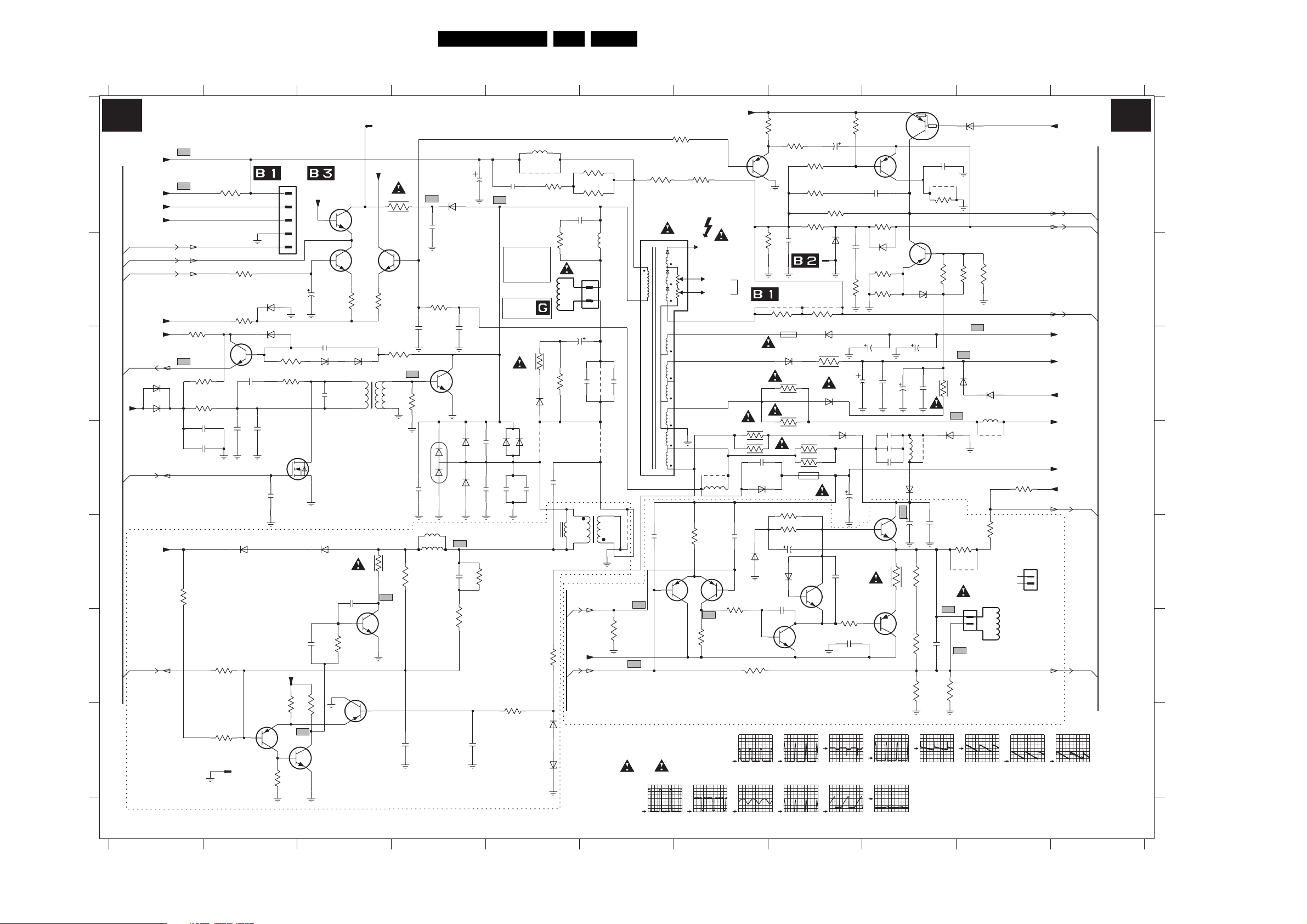
Circuit Diagrams and PWB Layouts
28L04E AC 7.
Mono Carrier: Deflection
1234567891011
7482
3476
2K2
6450
BAS316
3478
6K8
3486
6K8
2458
2490
-0V8
7453
BD136
5V / div DC
20µs / div
5V / div DC
5ms / div
2V6
*
24V
3n3
47n2456
3466
PDTA114ET
0V
17V1
16V 470u
2484
47n2XXX
6454
F462
2465
1R
-1V1
-12V4
1V7
1V7
6480
BZX79-B5V1
*
2455
RES
2480
220u
5404
RGP10D
2470
22u 100V
3467
3468
3471
20 V / div DC
7481
BC857B
18V1
100n
9404
220R
220R
2467
3R3
5ms / div
7V9
2483
47n
4492
3492
56K
3482
3481
6455
RGP10D
1u0
F458
15n
3472
6482
BZX384-C6V8
3K3
3494
F452
F453
6483
*
BAV21WS
F455
3437
2K0
4437
1451
F459
3R3
1V / div DC
5ms / div
RES
3483
BAV21WS
*
10K
6484
5451
9451
15K
3474
DEFLECTION COIL
3475
8K2
1XXX
B2P-VH
VERTICAL
500mV / div DC
5ms / div
POWER_DOWN
EHTinfo
A4
BCL
A4
EHTb
A2
-12V
VideoSupply
200V
Vbatt
Filament
+9V
-12V
Vguard
A4
Frame_FB
A2
500mV / div DC
5ms / div
A2 A2
LINE + FRAME DEFLECTION
F402
A
B
C
D
E
F
G
VT_Supply
VideoSupply
Filament
A2
A4
Frame_FB
A2
A4
+9V
HDRIVE
A4
EW_DRIVE
A4
EW DRIVE
Vbatt
EHTb
EHTinfo
-12V
+6VA
HD
6486
BAV21
6403
RGP10D
Vbatt
F401
F412
3499
3445
820K
BC847B
3489
47R
3414
*
2420
*
2414
1u0
7408
3418
100R
3495
3401
68K
1V
3402
1K0
3419
3K3
6V
2409
100n
2410
100n
6407
BAV21WS
3V6
1453
RES
To 1351 of
CRT PANEL
6490
BAS316
6443
BZX384-C12
-2V2
100n
2XXX
2408
7410
BC857B
From 1401 of
OR
CRT INTERFACE PANEL
1
2
3
1401
4
5
2493
3441
680K
3415
1K0
7404
SI2306DS
3
1
0V7
2
1n
2482
+9V
3420
3440
470R
F417
1V3
0V2
4K7
3498
+9V
7485
BC847B
50V4u7
100p2486
6441
68V
2489
4V5
6408
BAV21WS
10n
820K
7484
BC847B
7401
BUH2M20AP
3447
6442
1
10n
3
2488
100p
0V6
3446
470R
3V3
BC857B
7406
KTC2800
1402
+9V
3407
390R
5402
PSD10-204B
3497
2V8
7411
From LOT 5450
(For A80ERF042X14
Tube Only)
3411
F433
680K
7403
BC847B
68R
2402
3430
7405
680K
BU4508DX
F418
3425
2425
3416
2411
100K
RES
0V
33R
*
5403
5405
5
6
1R0
F416
27V6
2405
33n
6404
35m
3409
1K8
K
A
6401
BYD33V
2KV
1n
0V
DMV1500M
AK
F423
2403
126V
*
*
2487
3431
33n
6412
6411
1n0
100K
2428
2404
2412
BYV29X-500
2413
BYV29X-500
3436
*
56n
47u
F414
HORIZONTAL
DEFLECTION
To 1404 of
*
6410 RGP10D
*
2416
2427
15n
COIL
6491
*
3427
1K5
*
OR
BY228-1500
*
2492
5410
27u
9410
3404
6406
3432
22R
3412
4R7
3XXX
RGP10D
9401
*
2419
*
3428 2R2
6488
BAS316
6489
BZX384-C33
3433
220R
3434
220R
2406
680p
1K0
1404
2415
100V2u2
15K
2417
5408
12
5406
CI-15
SC21329
VDRA
A4
-12V
VDRB
A4
FRAME DEFLECTION
3488
10K
3451
*
LOT
5450
L.LIN
2418
3460
*
3
1
*
9407
2461
*
0V8
F460
2K2
F461
F401 130V / div DC
F402 32V8 / div DC
F452 -13V4 / div DC
F453 190V8 / div DC
I416 I417 I468I423 I433
20V / div DC
20µs / div
5401
*
1
4
9417
*
9402
1n
7455
BC857B
-12V4
10
6
5
11
7
12
8
9
3452
*
EHT
TO PICTURE TUBE
2K2
3462
1V4
F468
3463
500mV / div DC
20µs / div
+9V
7480
BC857B
0V
3480
3453
0V5
2K2
3487
33R
*
*
2451
TO 1382 of
3491
56K
3477
RES
3454
8K2
2481
3473
680K
1470
50V10u
6451
22K
3490
7483
BC857B
6V2
2491
RES
16V1u0
2453
BZX384-C4V7
FOCUS
3493
6452
6459
2460
220p
3470
22R
2469
220n
5V / div DC
20µs / div
5ms / div
RES
2454
16V 470u
2457
470u 16V
-0V6
-1V6
4u7
7451
BD135
VG2
9452
5452
-12V4
To
3456 1R0
2459
1n
2462
0V8
7456
BC857B
3469
1K0
1K0
3461
F412 F414 F460 F461
2V / div DC
20µs / div
10V / div DC
20µs / div
1R03422
6456
RGP15G
6457
-11V8
2K2
470p
BAS316
of CRT PANEL
3442
6K8
1454
1R
MRT
6453
RGP10D
3484
*
3485
*
330R3465
3464
330R
50V 100u2463
6458
2464
470p
-12V4
200V / div DC
20µs / div
10V / div DC
20µs / div
4R73423
3459 4R7
1452
MRT
1R
7454
BC847B
BAS316
-1V9
7452
BF422
9XXX9XXX
3443
6K8
RGP10D
3458
4R7
6481
1N4148
RGP10D
2468
0V5
F418 F455 F458 F459
I462
10V / div DC
3139 123 5676.5
F_16120_002.eps
121205
1401 A3
5408 D6
1402 A3
5410 A5
1404 B5
5450 B6
1451 E10
5451 C10
1452 D8
5452 D7
1453 G2
6401 A4
1454 B8
6403 C1
1470 B8
6404 D4
1XXX E10
6406 C5
2402 C4
6407 E2
2403 C4
6408 E3
2404 A4
6410 D5
2405 A4
6411 D4
2406 A6
6412 D4
2408 D2
6441 C3
6442 C3
2409 C2
6443 C2
2410 D2
6450 B9
2411 D4
A
B
C
D
E
F
I
G
2412 D4
2413 D4
2414 D2
2415 C6
2416 D5
2417 C6
2418 C6
2419 D5
2420 D2
2425 G4
2427 A5
2428 G4
2451 B8
2453 B8
2454 C9
2455 C9
2456 D9
2457 C8
2458 C9
2459 D7
2460 D8
2461 E6
2462 E7
2463 E8
2464 E8
2465 E9
2467 F9
2468 E8
2469 F8
2470 E9
2480 C9
2481 A8
2482 F3
2483 A9
2484 C9
2486 C3
2487 E4
2488 E3
2489 C3
2490 D9
2491 A9
2492 D5
2493 B3
2XXX D2
2XXX D9
3401 A2
3402 B2
3404 C5
3407 B3
3409 B4
3411 A4
3412 B5
3414 C2
3415 C2
3416 C4
3418 F2
3419 B2
3420 G2
3422 D7
3423 D8
3425 E4
3427 G5
3428 F5
3430 C4
3431 F4
3432 A5
3433 A6
3434 A6
3436 E4
3437 E10
3440 G3
3441 C2
3442 B8
3443 B8
3445 C1
3446 F3
3447 B3
3451 A6
3452 A7
3453 B7
3454 A8
3456 D7
3458 C8
3459 D8
3460 F6
3461 F7
3462 E7
3463 F7
3464 E8
3465 D8
3466 E9
3467 E9
3468 F9
3469 E7
3470 F8
3471 F9
3472 F9
3473 A8
3474 E10
3475 D10
3476 A9
3477 A8
3478 B9
3480 A7
3481 C9
3482 B9
3483 B10
3484 C8
3485 C8
3486 B9
3487 A8
3488 A7
3489 C2
3490 A8
3491 A8
3492 A9
3493 B8
3494 B10
3495 G2
3497 E3
3498 G2
3499 E1
3XXX C5
4437 E10
4492 A9
5401 B6
5402 C3
5403 E4
5404 D9
5405 E4
5406 E5
6451 B8
6452 C8
6453 C8
6454 D9
6455 D9
6456 D7
6457 E7
6458 E8
6459 D8
6480 B9
6481 C8
6482 A10
6483 C10
6484 C10
6486 C1
6488 G5
6489 G5
6490 B2
6491 D5
7401 A3
7403 B4
7404 D2
7405 C4
7406 F3
7408 C2
7410 G2
7411 G3
7451 D9
7452 F8
7453 F9
7454 E8
7455 E6
7456 E7
7480 A7
7481 B9
7482 A9
7483 A8
7484 G3
7485 B3
9401 D5
9402 D6
9404 D9
9407 E6
9410 A5
9417 C6
9451 D10
9452 D7
9XXX B8
9XXX B8
1234567891011
 Loading...