

Page 1
PHILIPS TECHNICAL TRAINING
L05HD TRAINING MANUAL
PHILIPS CONSUMER ELECTRONICS
64 PERIMETER CENTER EAST
PO BOX 467300
ATLANTA, GA 31146-7300
MM032205
Page 2

TABLE OF CONTENTS
INTRODUCTION . . . . . . . . . . . . . . . . . . . . . . . . . . . . . . . . . . . . . . . . . . . . . . . .1
POWER SUPPLY . . . . . . . . . . . . . . . . . . . . . . . . . . . . . . . . . . . . . . . . . . . . . . .4
AUXILIARY POWER SUPPLY . . . . . . . . . . . . . . . . . . . . . . . . . . . . . . . . . . . . . .5
MAIN POWER SUPPLY . . . . . . . . . . . . . . . . . . . . . . . . . . . . . . . . . . . . . . . . . . .7
DEFLECTION SYNC . . . . . . . . . . . . . . . . . . . . . . . . . . . . . . . . . . . . . . . . . . . . .9
TV SIGNAL PROCESSOR . . . . . . . . . . . . . . . . . . . . . . . . . . . . . . . . . . . . . . . . . 10
DEFLECTION . . . . . . . . . . . . . . . . . . . . . . . . . . . . . . . . . . . . . . . . . . . . . . . . . .10
CONTROL . . . . . . . . . . . . . . . . . . . . . . . . . . . . . . . . . . . . . . . . . . . . . . . . . . . . .13
VIDEO SIGNAL FLOW . . . . . . . . . . . . . . . . . . . . . . . . . . . . . . . . . . . . . . . . . . .15
CRT DRIVE . . . . . . . . . . . . . . . . . . . . . . . . . . . . . . . . . . . . . . . . . . . . . . . . . . . .18
AUDIO . . . . . . . . . . . . . . . . . . . . . . . . . . . . . . . . . . . . . . . . . . . . . . . . . . . . . . . .21
SIDE JACK PANEL . . . . . . . . . . . . . . . . . . . . . . . . . . . . . . . . . . . . . . . . . . . . . .23
TROUBLESHOOTING TO PANEL LEVEL . . . . . . . . . . . . . . . . . . . . . . . . . . . . .23
Page 3

Introduction
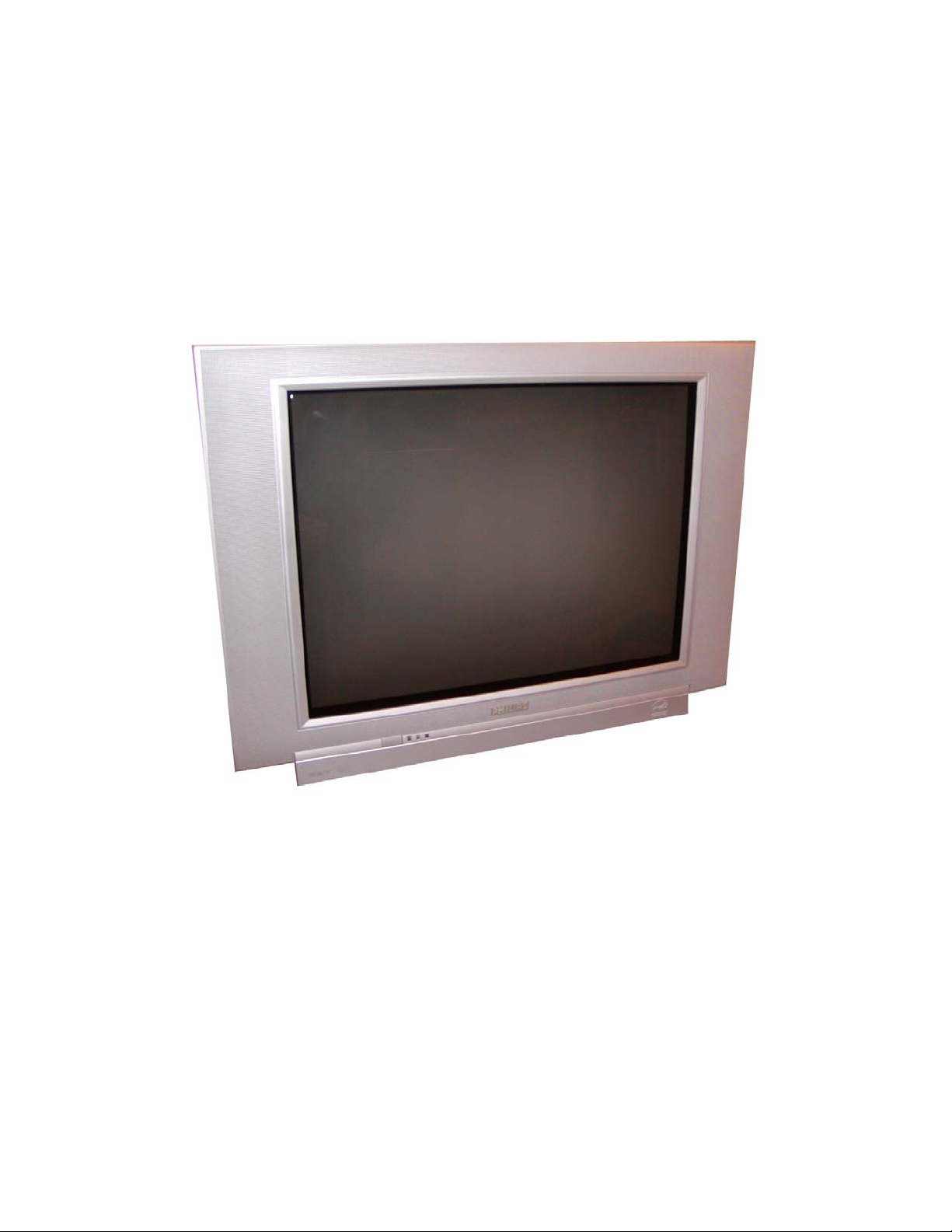
The L05HD TV chassis is designed for the model year 2005. This set is High Definition ready
with an NTSC tuning system. To receive the ATSC channels a set top box is required.
This design is used in large screen sizes of 27 and 30 inch with the 27-inch having a 4:3
aspect ration and the 30 inch version having a 16:9 aspect ratio. There are three types of
CRTs used which are the 100 degrees, 110 degrees, and wide screen version.
The standard architecture consists of a Main panel (called the family board), a Picture Tube
panel, a Side I/O panel, a HDMI panel, a HD panel, and a Top Control panel. The panels
consists primarily of conventional components with some surface mounted devices.
The functions for 1fH video and audio processing is performed in one IC (TDA1200xx, IC
7200), the Hercules chip. This chip is located on the solder side of the main panel.
The functions for the HD signals and 1fH to 2fH conversion is performed on the HD panel.
Except for switching, OSD, Closed Caption, Text, and A/D conversion, the bulk of the processing is performed by the Trident chip, IC 7201.
The L05HD chassis has two signal processing sections, one for the 1fH (NTSC), and one for
2fH (HD) processing. Whatever signal is applied to the set, it is displayed on the CRT in a
1080i format.
The NTSC tuning system features 181 channels with on-screen display. The main tuning
system uses a tuner, a microcomputer, and a memory IC mounted on the main panel. The
microcomputer communicates with the memory IC, Remote Receiver, Tuner, Signal processing IC, and HD processing section. The Memory IC retains the settings for favorite stations,
customer-preferred settings, and circuit settings. The circuit settings can be accessed by the
service technician via the Service Alignment mode.
The On-screen graphics and Closed Caption decoding are done within IC 7206 located on
the HD panel. They are added to the main signal in the Display Processor, 7221, located on
the HD panel.
Customer Operation
The L05 customer menu is similar to the L04 customer menu. The L05HD does not have
Picture-in-Picture.
Press the Menu button to make a selection. Press the Cursor up-down buttons on the
remote to highlight the desired selection. Press the right Cursor button to make the selection.
Page1
Page 4
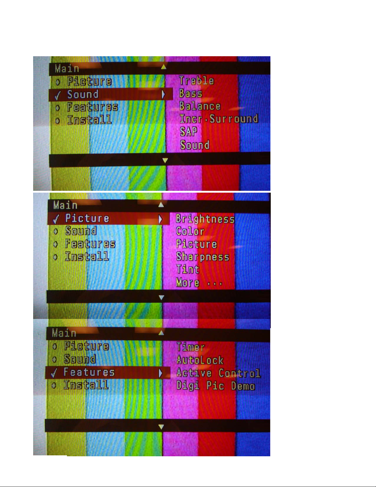
Press the Menu button on the remote and press the Cursor up-down button to obtain the
following screens.
Page 2
Page 5
VOL
1
3
5
6
7
2
4
Main
Picture
Sound
Features
Install
Timer
Rotation
AutoLock
Active Control
Digi. Pic. Demo
Features
Timer
Start Time
Stop Time
Channel
Activate
Display
Access Code
- - - -
AutoLock
Block Channel
Setup Code
Clear All
Block All
Movie Rating
TV Rating
Of fStop T ime
Channel
Activate
Display
Access Code
XXXX
Incorrect
New Code
- - - -
Confirm Code
XXXX
Timer
Rotation
AutoLock
Active Control
Digi. Pic. Demo
Access Code
XXXX
Features
T imer
Rotation
AutoLock
Active Control
Digi. Pic. Demo
Features
T imer
Rotation
AutoLock
Active Control
Digi. Pic. Demo
Features
T imer
Rotation
AutoLock
Active Control
Digi. Pic. Demo
Features
T imer
Rotation
AutoLock
Active Control
Digi. Pic. Demo
Features
Timer
Rotation
AutoLock
Active Control
Digi. Pic. Demo
2
4
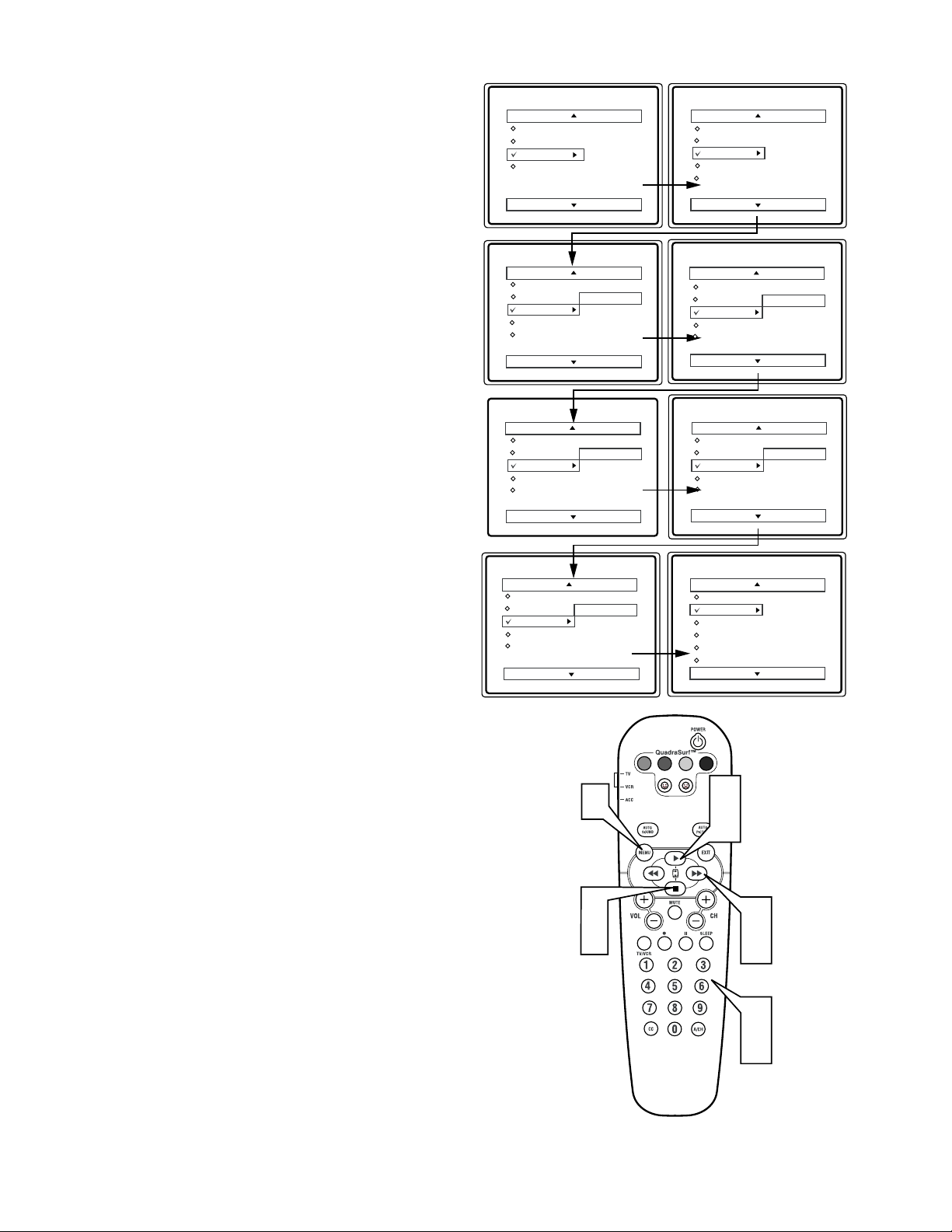
Setting up the access code.
1. Press the Menu button on the remote
to display the on-screen menu.
2. Press the Cursor up or down buttons
until the word features are highlighted.
3. Press the Cursor right button to display
the features menu options.
4. Press the Cursor up or down buttons
until the words autolock are highlighted.
5. Press the Cursor right button. The
screen will read, “Access Code ----”
6. Using the number buttons, enter 0, 7,
1, 1. XXXX will appear as you press
the buttons.
Incorrect code will appear on the screen.
Enter 0711 again.
7. The screen will ask you to enter a new
code. Enter any 4 digit code.
Page 3
Page 6
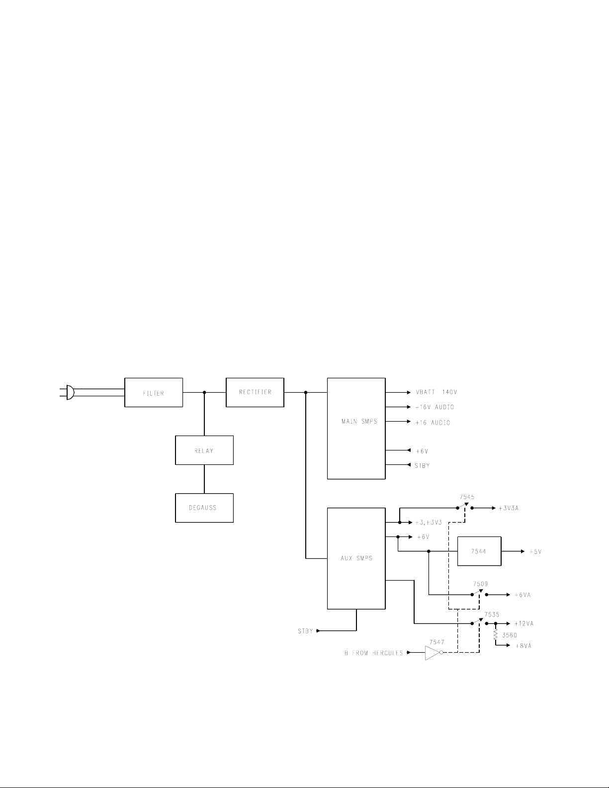
Power Supply Block (Figure 1)
The Power supplies are both located on the Family board. The supplies are divided into two
sections, the Auxiliary and Main section. A single filter and rectifier circuit supplies both
sections. The Auxiliary supply operates in a low power mode when the load is reduced. In
the standby mode, the 3.3 and 6 volt supplies are operating. The 3.3 volt supply provides
power to the processor section of the Hercules. The 6 volt supply provides power to the IR
receiver. The Main supply is switched Off via the Standby line.
When the set is turned On, the "B" line from the Hercules processor goes High switching
7547 which turns 7535, 7509, and 7545 On. The +3V3A, +6VA, +12VA, and +8VA supplies
are then switched On. The load placed on the Aux Power supply will cause it to switch to the
full power mode. At the same time, the STBY line switches Low turning the Main SMPS
supply On. The supply produces a +6 volt, +140 volt, -16 volt, and +16 volt supplies.
The +Vaudio (+16 volt) supply switches on the degauss relay.
Page 4
FIGURE 1 - POWER SUPPLY BLOCK
Page 7

Auxiliary Power Supply (Figure 2)
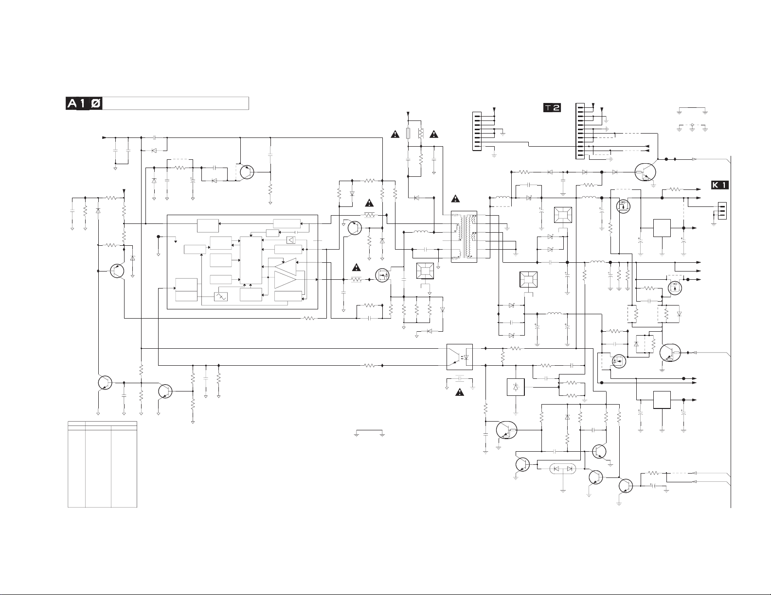
IC 7510 is the heart of the Auxiliary Power supply. In the Standby mode, VIA the current
sensing and Control circuits, a low power condition is detected by the IC. The IC then goes
into a Burst Mode operation to reduce the power used by the circuit. In the Burst Mode, the
supply will operate at approximately 25 kHz. In full power operation the frequency will be
approximately 66 kHz.
When power is first applied to the set, Start up is supplied to the IC by the internal Start-Up
current through Pin 14. Startup voltage is also applied to the IC to Pin 2 by the AC_IN line
which is tied to the neutral side of the AC line. During normal operation, power is supplied to
the IC by the HOT windings, Pins 1 and 2, of transformer 5504. Output drive from Pin 11 is
applied to the Gate of Transistor 7525. Voltage developed across the current sensing resistors in the Source of 7525 provides current sense information to the IC. When 7525 is
switched Off, the voltage on Pin 1 of 5504 goes High. This winding supplies the operating
voltage the power supply circuit. It also turns Transistor 7567 On causing the Gate of 7525 to
stay Low as long as Pin 1 of 5504 is High. This prevents 7525 from turning On until the field
of 5504 has collapsed.
Regulation is accomplished by monitoring the +3 volt supply. This voltage is fed to Shunt
regulator 7542 which controls the current through opto-isolator 7516. Shunt Regulator 7542
begins conducting when Pin 3 of the IC reaches 2.5 volts. At this point current flows through
the opto-isolator, 7516. The transistor inside 7516 turns On applying a control voltage to Pin
6 of 7510. If a problem should develop in the feedback circuit causing an excessive voltage
on Pin 6, Transistor 7549-2 will turn On, switching Transistor 7532 On. This will a voltage to
the Demag circuit on Pin 7 causing the IC to latch Off. The IC will stay latched until power is
removed and reapplied to the set.
In the Standby mode, the "B" control line from the Hercules Processor is Low. Only the +3,
+3V3, and +6 volt supplies are present. When the set is turned On, the "B" line will go High,
turning Transistors 7509, 7545, and 7535 On. This will switch On the +8VA, +12VA, +8V,
+3V3A, +6VA, and +5V supplies.
In normal operation, voltage from Pin 12 of 5504 is rectified by 6540 to produce a negative
voltage which prevents Transistor 7561 from turning On. If AC is removed from the set, this
negative voltage will disappear. The voltage across the filter capacitors on the +3V line will
turn 7561 On. The Power Down line will then go Low signaling the processor to shut the set
down.
Page 5
Page 8
COM
OUTIN
KA
REF
COM
OUTIN
Vcc
Gnd
Ctrl
START-UP
CURRENT SOURCE
VALLEY
START-UP
CURRENT SOURCE
CURRENT
SENSING
OUTPUT
DRIVER
OVER
POWER
LOGIC
CONTROL
CIRCUIT
MAXIMUM
ON-TIME
PROTECTION
VOLTAGE
CONTRLLED
OSCILLATOR
OVER
TEMPERATURE
PROTECTIOM
POWER-ON
RESET
SUPPLY
MANAGEMENT
FREQUENCY
PROTECTION
CONTROL
INPUT
CONTROL
CIRCUIT
BURST
DETECTOR
Drain
HVS
Sense
Demag
Driver
*
0V
300K
S
20V
470U
I564
0086
HEATSINK
6
A4
E
15V8
15V9
10V
1M5
A4
470U
6548
2522
470p
3599
To 1405
Of
Deflection
Controller
*
*
*
1V3
9
*
5V7
TEA1507
---
JMP
3V4
C
E
158V
C
4V5
3V4
E
0V
B
REGION
3540
27VRF-HD
---
---
*
JMP
AUXILIARY POWER SUPPLY
1V5
2
G
C
*
0V1
E
0V
B
3V4
3m3
7
3
E
0V7
E
158V
0V
*
E
0V
C
E
B
C
B
3V7
Microcontroller
B
11
*
2V5
C
9V
4m7
A4
15V8
0V6
B
6V
8V1
330K
B
15V8
To 1533 Of
Source Select +
*
*
3V2
0V
C
0V
*
E
B
2V
**
0V
*
D
A4
14
B
0V
E
C
0V
0V7
*
*
*
*
*
*
*
*
0V
B
C
10V7
B
*
C
*
0V
E
B
C
0V6
8V
C
E
9V
*
6V3
*
9530
9534
NAFTA
30WSRF-HD
---
---
---
---
SIZE
3548
3551
3566
4523
4540
4548
4551
4566
4585
5523
6553
7535
9515
9524
9529
---
---
Vaux_GND
+3V3
AUX_ON|ITV_MSG
POWER_DOWN
+8V
+12VA
Vaux_GND
Vaux_GND1
100MHZ 120R
BAS316
SI2307DS-E3
---
---
---
---
---
---
---
---
---
---
---
JMP
---
JMP
---
---100MHZ 120R
BAS316
SI2307DS-E3
---
---
---
---
---
9534
Vaux_GND1
Vaux_GND
Vaux_GND
7561
I537
3537
68K
PDTC143ZT
I594
I596
6512
BZX384-C18
68K
3546
22u
2510
F578
2591
1n0
470p
2539
3568
47K
1n0
2524
3548
68K
I536
I556
I532
Vaux_GND
3581
22K
I526
BAV21WS
6537
Vaux_GND1
2590
BC847BW
7584
F584
10n
2575
BZX384-C15
6549
BAV21WS
6532
6545
SB340L-7010
2526
100n
13
Vaux_GND1
L78L33ACZ
7544
2
10K
3593
1000mAT
1532
I558
2584 470u
2564
9509
100n
I512
68K
3540
I554
4585
I553
7535
SI2307DS
Vaux_GND
5
6
7
8
16V47u
2558
1534
1
2
3
4
Vaux_GND
F535
10K
3591
220R
3563
6540
BAS316
4566
2K2
BAW56W
3536
Vaux_GND
2586
330p
9529
BAS316
6531
BC857B
7532
I533
I545
RGP10D
6533
33K
Vaux_GND
5521
3592
IMX1
12
MainSupplyGndA
Vaux_GND
7549-2
7
8
9
HEATSINK
0088
1
10
11
12
2
3
4
5
6
12
1533
BAS316
6534
3587
2K2
2580
10n
I509
3532
I588
3529
1K2
3560
33R
BC847BW
7577
BAV21WS
6538
3538
Vaux_GND
2523
1n0
I589
6546
STPS10L60D
100n
2543
HEATSINK
0083
12
BAS316
6543
5523
4551
I538
I599
I563
I592
3528
4M7
I534
3585
68K
3535
7545
3
1
2
4R7
SI2305DS
3544
2K2
I557
9523
100n
2520
SB340L-7010
6544
7583
BC847BW
5526
IMX1
7549-1
BZX384-C12
Vaux_GND1
3594
6542
4548
22K
3586
5K6
82K
I510
3590
I547
Vaux_GND
Vaux_GND
Vaux_GND
4523
I565
3534
F577
3533
1
4
3
2
7516
TCET1103(G)
Vaux_GND1
Vaux_GND1
Vaux_GND
BZX384-C6V8
6547
3588
470K
1n0
2538
F534
7575
PDTC143ZT
2579
10n
I593
Vaux_GND1
F582
100n
2576
4540
220R3561
5527
Vaux_GND
9524
3525
47n
2521
2588
2589
2u2
Vaux_GND
1m0
2536
F537
Vaux_GND1
3562 220R
9554
4567
I539
Vaux_GND1
I568
PDTC143ZT
680R
3542
7547
470u
2587
3549
270R
Vaux_GND
Vaux_GND
BC857B
3583
5K6
7585
3596
10K
2525
470p
2585
1u0
470u
2534
16V
BAS316
6554
BAS316
6553
SARS03
6550
2578
1n0
2544
2n2
I540
Vaux_GND1
F581
I595
F585
2582
100n
3527
47K
3565
15K
2546
2u2
Vaux_GND
2557
47u 16V
Vaux_GND1
9515
7567
BC847B
Vaux_GND
3595
100K
7525
10u
2583
3539
1K0
3550
220K
7510
3547
68K
3K3
3567
Vaux_GND
F580
9
2577
100u
10
11
12
2
4
5
6
7
8
SS28411-00
5504
1
3553
27K
3543
10K
STPS10L60D
6552
56K
3530
I590
I529
2528
470n
Vaux_GND
2K2
3545
F586
I528
I531
3589
10K
Vaux_GND1
3551
4R7
1
2
3
MAINSUPPLYGND
1535
6539
SB340L-7010
7576
BC847BW
I560
2535
I597
3526
68K
3566
3597
47K
68p
2592
SI2307DS
7509
5524
10u
9536
2
1
3
3531
1K0
TL431CZ-AP
7542
Vaux_GND1
I530
BAS316
6536
3598
Vaux_GND1
Vaux_GND1
F583
2556
47u
9530
16V
2
13
2555
47u 16V
7543
L78L33ACZ
+3V
+5V
+8VA
Stdby_con
+6VA
+5V
+3V3A
+6V
+6VA
VDC
+3V3A
+8V
AC_IN
VCC
+3V3A
B
1.27V On
1.45V Off
15.5 On
11.5 Off
21 On
11.8 Off
Page 6
FIGURE 2 - AUXILIARY POWER SUPPLY
Page 9
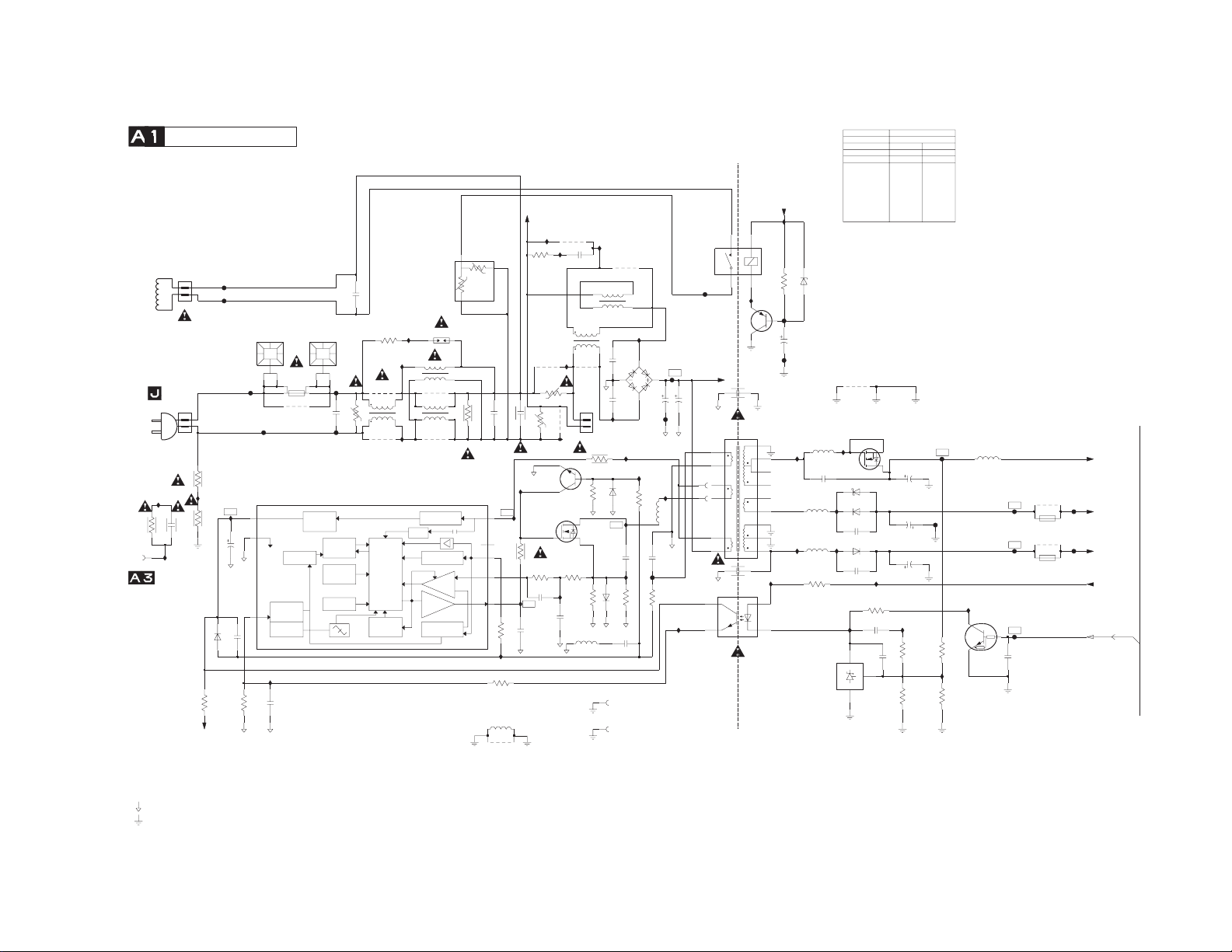
Main power supply (Figure 3)
The Main Power supply provides the VBAT (141 volt), and Audio voltage supplies. This sup-
ply is switched Off during the Standby mode. During Standby the STBY_Con line is High
which turns Transistor 7573 On. This causes the opto-isolator 7513 to turn On hard. This
places a higher voltage on the control Pin of IC 7511 causing the IC to shut down. The
operating voltage from the Auxiliary supply keeps a small voltage on Pin 2 of 7511 to prevent
it from cycling On and Off. Output from Pin 11 of 7511 drives FET 7512 which drives
Transformer 5512. When Pin 2 of 5512 goes High, Transistor 7514 is switched On turning
7512 Off. This is to prevent 5512 from becoming saturated.
When the set is turned On, the STBY_Con line goes Low switching 7573 Off. The VBAT
supply is the reference voltage for regulation. Since this voltage is missing during startup, the
Shunt Regulator 7571 is turned Off. The voltage on Pin 6 of 7511 goes Low, which turns the
drive from the IC On. When the set is On during normal operation, the supply voltage on Pin
2 of the IC is supplied by Pin 2 of Transformer 5512. When the VBAT supply reaches the
correct voltage, Pin 3 of the Shunt Regulator 7571 reaches 2.5 volts switching it On. This
switches the opto-isolator On to provide a regulation feedback path.
Transistor 6551 provides a power on ramping of
the VBAT supply.
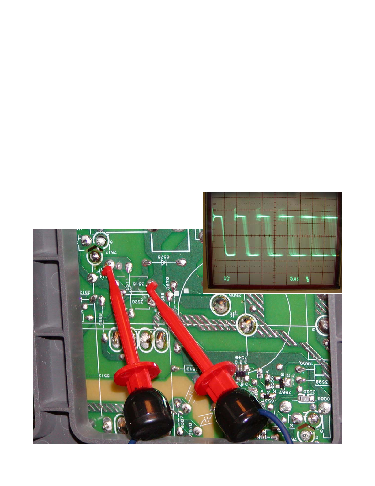
7512 drive test points.
Page 7
Page 10
-T
V
-T
+T
Rs
Rh
KA
REF
Vcc
Gnd
Ctrl
START-UP
CURRENT SOURCE
VALLEY
START-UP
CURRENT SOURCE
CURRENT
SENSING
OUTPUT
DRIVER
OVER
POWER
LOGIC
CONTROL
CIRCUIT
MAXIMUM
ON-TIME
PROTECTION
VOLTAGE
CONTRLLED
OSCILLATOR
OVER
TEMPERATURE
PROTECTIOM
POWER-ON
RESET
SUPPLY
MANAGEMENT
FREQUENCY
PROTECTION
CONTROL
INPUT
CONTROL
CIRCUIT
BURST
DETECTOR
Drain
HVS
Sense
Demag
Driver
9V3
*
HOT GROUND
D
RES
15V5
HOT
G
*
TUNER IF
Front Interface Panel
6
*
FOR MAINS 120V AC 170V (177V)
100n
*
*
14
*
*
RES
(For
TEA1506T/N1
2V3
..V.. Normal Operation
POWER SUPPLY
*
160V
0V
T4E.250V
Lightning Protection
Vbat
AUDIO OUTPUT
1572
"$"
140V
Provision For
15V6
COLD
*
0R1
3
7
*
16V4
2506
33n
*
*
*
*
RES
*
LKS1AF
0V
DEGAUSSING COIL
*
9
SET
MAIN RANGE
REGION
For ITV only
*
Provision For
RES
*
0V
0V
AC Main Plug
Or
From 1505 Of
For EMC
470P
2X10w
---
---
---
---
---
--JMP
JMP
JMP
---
---
---
---
---
--JMP
JMP
JMP
*
+16V
1577
2506
5500
9502
9504
9506
2
*
*
297V
*
COLD GROUND
(..V..) Standy Mode
For ITV Only
1n5
TO 1013 OF
RES
8V2
295V
1n5
*
2V3
-16V
Protection)
*
2V2
RES
16V4
RES
*
RGP10D
Lightning Protection
"$"
S
8V2
11
0V
Lightning
A4
*
9577
9572
5V
143V
30WSRF-HD
2X10w
143V
27VRF-HD
LR
NAFTA
1502
PFC5000
AUDIO_GND1
1546
-Vaudio
+Vaudio
AC_IN
9572
2
1
3
BAS316
6514
6551
STPS10L60D
6564
I525
I543
100n
2516
47K
3541
I542
5561
100u
2552
6563
I584
I583
3579
F562
2K2
5564
1
4
23
45
81
DMF2405H60
I501
5502
I513
9506
I561
3500
3M3
3516
2505
5
8
9
13
14
15
16
17
18
2
3
4
5512
10
11
12
1M5
3504
2503
2n2
I502
F573
1K0
3515
F503
I527
Audio_Gnd
2502
PFC5000
1501
1
2
3M3
1505
F506
3501
22u
5563
AUDIO_GND2
1510
2574
1n0
1500
9513
9512
3509
2R0
2n2
2504
I522
9511
TCET1103(G)
7513
14
3
2
3508
220R
7512
22u
2511
2562
50V
F563
470p
2565
F541
I562
3520
I582
I521
I581
I552
I580
1
3
2
7571
TL431CZ-AP
2
1507
1
3523
3
2
1
4R5
4R5
2541
47u 25V
9503
2508
100n
1N5062
5551
6575
27u
5552
3502
I505
PDTC114ET
7573
F509
3519
15K
9510
MainSupplyGnd
47K
3522
2518
10n
I515
I508
3574
7511
I511
15n
2571
2542
F501
F552
3524
47K
9505
I576
F504
3575
82K
3K3
AUDIO_GND1
3521
3573
15K
BC857B
7541
1n0
2517
3571
F502
MainSupplyGndA
I551
9500
2515
470p
5511
F500
I573
I578
AUDIO_GND2
I574
2K2
3513
4K7
3576
I520
I519
F507
6511
I514
AUDIO_GND1
Vaux_GND1
F510
6562
9563
F508
F542
2512
3M3
3506
4R73511
F564
F565
9577
1577
2.5AF
I506
I579
2551
1n0
2563
2501
100p
2519
2.5AF
1572
I571
F561
5562
3505
2570
2507
10n
2572
3510
7514
BC847B
3517
330K
2R0
1K2
I524
I572
3512
I517
BZX384-C12
6541
23
5500
14
2514
I523
2561
1n0
3518
9502
Vaux_GND1
3K3
9501
1
4
23
I518
DMF2405H60
5501
1503
341
2
AUDIO_GND2
470n
I507
2500
1
4
9504
6500
23
5506
14
23
1
2
DMF35
1504
3514
3503
DSP-301N
2509
2513
470p
1545
I516
5513
1u0
VCC
Stdby_Con
+Vaudio
VDC
Vbatt
+6V
14 On
2.8 Off
0.6V Off
1.3V On
Page 8
FIGURE 3 - MAIN POWER SUPPLY
Page 11
Deflection
AD
PS
RESET
ADDRSEL
ALE
WR
RD
SD
SC
INT
IRSET
HFLB
VPROTHSYNC
VSYNC B
G
R
VM
7
6
5
4
3
2
1
0
T3
T3
T2
T2
2V5
1V5
2V2
T3
2V5
2V5
2V5
2V5
*
3V3
0V
2V4
2V4
2V4
2V4
3V
3V
3V3
1V3
2V4
0V
0V
T1,T5
T2
T3
T3
T1,T5
T3
T2,T5
T2,T5
T2
T3
T3
T3
T2
2V5
2V5
Sets w/o PP
T3
T1,T5
T5
T5
T1,T5
2V5
*
T1,T5
0V
0V
0V
0V
*
*
*
3V
T5
2V5
T3
2V5
2V5
2V5
1V9
2V5
2V5
0V
2V5
3V3
2V5
2V5
2V5
2V5
2V5
220R
F208
3203
26
37
35
176
28
36
34
180
31
6
27
177
5
179
178
171
170
169
168
167
166
165
4
175
29
6930 DPTVSVP
& DDP
DAC
CPU
7201-2
172
560R
3221
AGND5
F287
2225
100n
7203
BC847B
BC847B
7204
2217
100n
100n
2220
4203
2224
100n
F207
3229
180R
3228
220R
3223
100R
220R3207
4202
2239
100n
2219
100n
2222
100n
7201-4
6930 DPTVSVP
3225
1K0
F288
150R
3227
3
9
8
7
4204
100n
2221
3202 10K
4n7
2246
68p
2242
3204 220R
1K0
3284
27p
2240
100R
3224
3230
75R
F290
F289
16V 22u
2263
3283
1K0
1u0
2241
2226
100n
2218
100n
2247
4n7
BC857B
7202
9
11 12
4209
10
100n
2223
220R3208
10K
3222
2243
68p
3206 220R
220R3205
HSYNC
+5V
+5V
CAPD17
CAPD16
CAPD23
CAPD22
CAPD21
CAPD20
CAPD19
CAPD18
SVM_PP
VM
RD
VSYNC
SDA_OUT
+8V
PSM
ALE
WR
SVM_ROT
DPTV_R
DPTV_G
DPTV_B
SCL_OUT
RESET
HS_9883
VS_9883
CLK_9883
VCC3
+3V3
VCC3
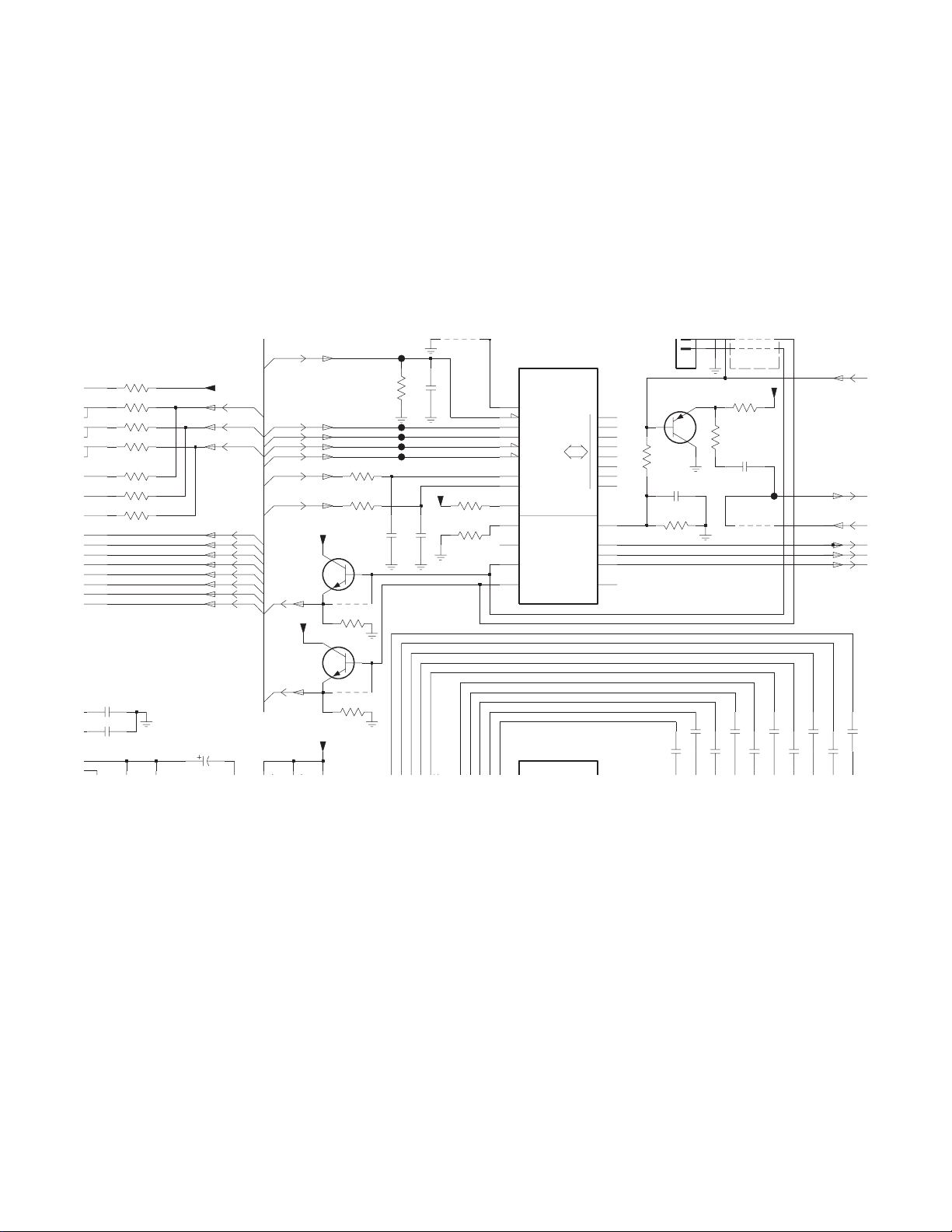
Sync (Figure 4)
Whatever signal is applied to the L05 chassis, it will display the picture in a 1080i format.
This means that the Line or Horizontal frequency is always 33.75 kHz. The Vertical or Frame
rate is 60 Hz.
Vertical Sync is output from the Trident IC 7201 on Pin 35. The signal is buffered by
Transistor 7203 before being fed to the TV display processor and TV Microcontroller. In the
same manner Horizontal Sync is output on Pin 34 and is buffered by Transistor 7204.
FIGURE 4 - SYNC
Page 9
Page 12

TV Signal Processor (Figure 5)
Red, Green, and Blue from the Trident IC is input on Pins 30, 31, and 32 of 7221, TV Display
Processor. The RGB/YUV matrix changes the signal to a YUV signal before feeding it to a
Color level control circuit. The signal is fed to the RGB insertion circuits where the OSD is
inserted. The signal is then fed to a White Point and Brightness Control circuit and then to
the CRT panel. The White Point and Output Amplifier have the Drive controls and Cutoff controls. Input from the ABL line on Pin 43 makes adjustments in the brightness levels to adjust
for changes in beam current. The Cutoff
pulses from the CRTs are fed to Pin 44 to the Cathode Calibration circuit. The Cathode
Calibration circuit adjusts the cutoff levels of the CRT to maintain the correct gray scale tracking. When the set is first turned On, a calibration pulse is output on the RGB lines. The
Cathode Calibration circuit monitors this pulse on the Cutoff line to set the Black level and the
maximum drive voltage for the cathode. Once the Calibration has taken place, the Output
Amplifier switches to the RGB drive signal as the output. Horizontal and Vertical Sync is fed
to 7600 on Pins 23 and 24. IC 7600 processes the sync to provide the geometry for the picture. Horizontal drive is output to the sweep circuit on Pin 8. Vertical drive is output on Pins 1
and 2. East West drive is output on Pin 3. Sandcastle (SCO) is output on Pin 9. Horizontal
Feedback (HFB) from the sweep circuit is fed into the Phase Loop to phase correct the
Horizontal drive. IC 7221 is controlled by the Hercules Processor on the Family Board via the
I2C buss on Pins 10 and 11. Transistors 7226 and 7227 levels shifts the I2C buss level
between 5 and 3.3 volts. Geometry and Drive settings are stored in the Memory IC located
on the Family Board.
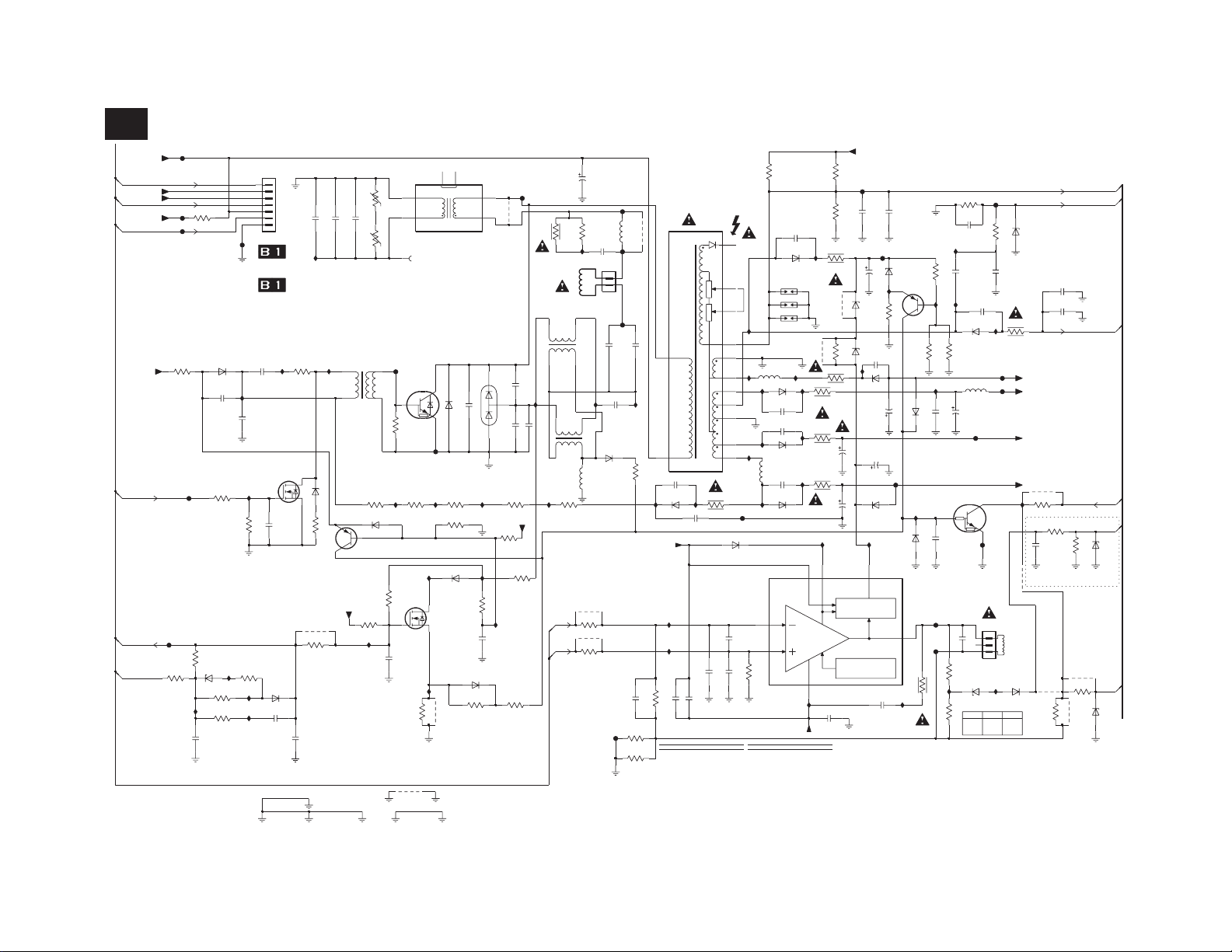
Deflection (Figure 6)
Horizontal drive from 7221 is fed to Transistor 7404 located on the Family board. This drive
circuit has two power sources. During startup, it is powered by the +6 volt supply. Once the
High Voltage circuit is running, it is powered by Pin 9 of the IFT. 7404 drives Transformer
5402 which drives the HOT (Horizontal Output Transistor). The HOT drives the IFT and the
Horizontal Deflection Coil. The IFT is powered by the VBAT (141 volt) supply.
The IFT produces High voltage, Focus voltage and G2 voltage to drive the CRT. In addition,
a 200 volt supply is produced to drive the CRT panel, a +14 and -14 volt supply for the
Vertical output, Filament voltage, +200 volt VideoSupply, and a +12V_lot supply.
Transistor 7408 monitors the IFT secondary to sense the presence of over voltage. If the
High Voltage goes High, the voltage on Pin 6 of the IFT will go High. When the voltage on
diode 6480 exceeds 15 volts, transistor 7408 will turn On. If 7408 turns On, it will turn 7407
On causing the x_ray protect line to go Low. The Processor will then shut the set down. In
addition the EW_DRIVE circuit is monitored. If the EW_DRIVE fails, transistor 7406 will turn
On constantly placing a dc voltage on the source. This will turn 7407 On.
IC 7451 is the Vertical Output IC. It is powered by the +14 and -14 volt supply from the IFT.
The Vertical pulse is rectified by 6458, keeping the V_PROTN line High. If the vertical output
should fail, the V_PROTN line will go Low. The Hercules processor will then shut the set
down.
Page 10
Page 13
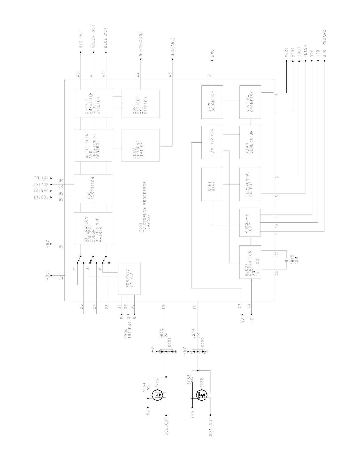
FIGURE 5 - TV SIGNAL PROCESSOR
Page 11
Page 14
G2
FOCUS
EHT
VV
NC
*
10KA51K
BU2527DX
*
G
4V6
14V9
D
0VC
S
0V
0V6
*
*
*
0V
0V6
A2
*
L.LIN
100R
6M8
13V9
*
2419
*
*
*
*
Or
TO 1351 OF
CRT Socket
RES
1K5
A5
100R
*
A4
A5
COIL
A5
A
COIL
1R5
*
For ATSC only
A5,B1
3432
A2,A5
126V
1u
*
2R2
TO 1351 OF
0V
*
HORIZONTAL
K
DEFLECTION
VERTICAL
0V
*
E5V7
B
DEFLECTION
A2
*
8n2
1R5
J
*
50V
TO PICTURE TUBE
*
S
2R7
D
7V
*
*
*
10K
*
ATSC
CRT Panel
22R
*
*
From 5450 Of LOT
(30PWXXXX Only)
G
*
*
3V6
50V7
0V5
2R7
6V
A5
A2
3432
*
3V3
12V7
*
**
*
B
0V
E0V
C
9442
*
A4
LINE + FRAME DEFLECTION
**
*
Tri+
E
42V4
C
A2,A5
45V7
B
**
*
-14V7
A2,A5
BAS316
6481
MainSupplyGnd
I419
3443
RGP10D
I464
6461
BSH103
7404
1403
F458
CRT_GND
F404
CRT_GND
3435
10R
DMV1500M
6404
MainSupplyGnd
I482
GND_EW
I424
2433
I453
3466
2413
9489
2421
3K9
F416
3474
6403
RGP10D
2417
470p
2459
3426
100K
2473
15n
100R
3418
1
2
4
3
VideoSupply
5408
3
5
6
7
8
9
I475
5450
1
10
11
12
F456
F418
2n2
2462
VSUP
2
VSUPO
6
TDA8177F
PROTECTION
FLYB
3
GND
4
IN+7
IN-1
OUT 5
7451
FLYBACK
GENERATOR
POWER
AMPLIFIER
THERMAL
3471
F482
2424
470p
9411
4R7
3415
2423
330p
1u0
2469
I413
5401
GND_DEF
I471
2431
2n2
6491
BZX384-C3V3
GND_EW
I463
1M0
3499
10K
3496
3421
1
2
3
4
5
6
7
I490
1401
1406
BYV27-200-TAP
6457
34243425
GND_EW
250V1u0
2436
1K5
3477
CRT_GND
GND_DEF
1
2
I427
2496
10n
1404
7406
6484
BAS316
I470
4418
I493
BAS316
6485
3473
9484
1K0
I426
3432
BYV27-200-TAP
6456
3455
1R0
F476
100n
2458
3442
22K
2
3
6442
BZV85-C6V8
1451
1
1402
F478
3434
1K0
9432
6483
BAS316
2491
2u2
Vbatt
82K
3431
3490
150R
1R0
3486
I488
2u2
2425
22K
3437
2
4
5
7
9
I414
CD25405-00
5456
1
PSD10-204B
5402
1
3
5
6
2474
150p
I428
10n
2472
RGP10D
6466
2499
1u0
-14V
4495
2478
15n
CRT_GND
BAS316
6487
BZX384-C8V2
6492
2404
47K3401
47u
I433
1
2
4
3
F465
5409
GND_EW
I431
CRT_GND
2418
VideoSupply
GND_HOR
CRT_GND
47u
2461
6482
BZX384-C6V8
CRT_GND
2407
100n
2471
6476
3n3
BZV85-C6V8
3458
4R7
I459
47R
3416
1n0
2432
F401
3460
68K
6488
BZX384-C33
CRT_GND
GND_HOR
9490
3478
10R
3472
2494 470p
3453
56K
100K
F453
3408
I455
F483
2u2
2466
100R
3489
470u
2449
CRT_GND
+12V_LOT
6453
5458
I466
RGP10G
CRT_GND
F457
3414
4R7
GND-LINEDRIVE
+12V_LOT
CRT_GND
470u
CRT_GND
VT_Supply
GND_EW
2460
5459
560n
150R
3413
3480
Vbatt
F452
GND_EW
3459
680K
3441
100R
I473
2412
2488
100n
I423
2464
2426
470p
10K
3497
6464
BZX384-C27
CRT_GND
GND_DEF
I465
10K
3438
I436
2448 470p
I425
7405
3427
680K
GND-LINEDRIVE
BZX384-C15
6480
3488
220K
I481
3493
GND_DEF
BYV29X-500
6467
2435
1K0
3481
GND_DEF
GND_HOR
Vbatt
BC857B
7410
CRT_GND
F459
GND_HOR
3439
10K
2451
BZV85-C6V8
6452
F481
4R7
3451
F402
2n2
2463
I430
2477
4434
CRT_GND
BC857B
7408
+6V
GND_HOR
3461
F461
I468
BAS316
6458
100n
2410
1405
F419
I494
I411
BZX384-C6V8
6434
3485
I415
9440
I489
5457
3491
33K
2467
220n
CRT_GND
I416
2454
470u
F455
I412
3433
4R7
RGP10D
6471
9476
I418
2470
220n
CRT_GND
1R0
3450
BAS316
6490
680K
3436
3428 22K
2411
I457
2468
100n
5452
10u
4401
3467
6489
BAS316
GND_EW
33n
2409
F472
GND_DEF
I410
I499
CRT_GND
I417
+14V
9402
2416
I492
3402
330R
22K
3469
6486
BYD33D
I469
4R7
3419
9435
I434
I432
2R2
3440
2495
100n
CRT_GND
2422
I435
I460
3468
3463
F462
3462
18K
CRT_GND
I462
3456
1R0
150R
3412
BZX384-C15
6449
F475
F464
GND_HOR
I458
CRT_GND
33K
3492
220n
2465
2493
GND_DEF
I440
470p
7407
I456
PDTC144ET
MainSupplyGnd
220p
2497
GND_EW
GND_EW
I461
470p
2492
Frame_FB
HFB
EHTinfo
Filament
EHTinfo
-14V
EHTinfo
Filament
X_RAY
HD
EW_DRIVE
Vguard
+12V_LOT
VDRA
V_PROTN
+14V
VDRB
SVM_ROT
F_15050_017.eps
A2
SIZE
REGION
100R
100V 100N
---
2KV 220P
1K6V 12N
630V 27N
---
---
250V 330N
250V 1U2
2KV 330P
2KV 330P
NAFTA
27VRF-HD
2KV 820P
1K6V 12N
630V 27N
2411
2412
2413
2413
2417
2418
2419
---
30WSRF-HD
2421
2422
2433
2451
3418
3424
3425
3434
3435
1MA 612V
1MA 612V
---
---
---
--250V 390N
250V 560N
---
--2KV 220P
100V 220N
100R
---
---
---
SIZE
REGION
---
3478
3489
4401
4418
5408
5450
5456
6476
9411
9435
9440
9442
9476
9489
NAFTA
27VRF-HD
---
820K
---
---
---
---
W7132-004 Y
JF0101-85039 B
---
BZV85-C6V8
JMP
JMP
---
JMP
---
---
30WSRF-HD
3442
3459
---
470K
---
---
---
---
W7131-003 Y
JF0101-85038 B
SD20417-02 Y
BZV85-C6V8
---
JMP
---
JMP
---
Page 12
FIGURE 6 - DEFLECTION
Page 15
Set Control (Figure 7)
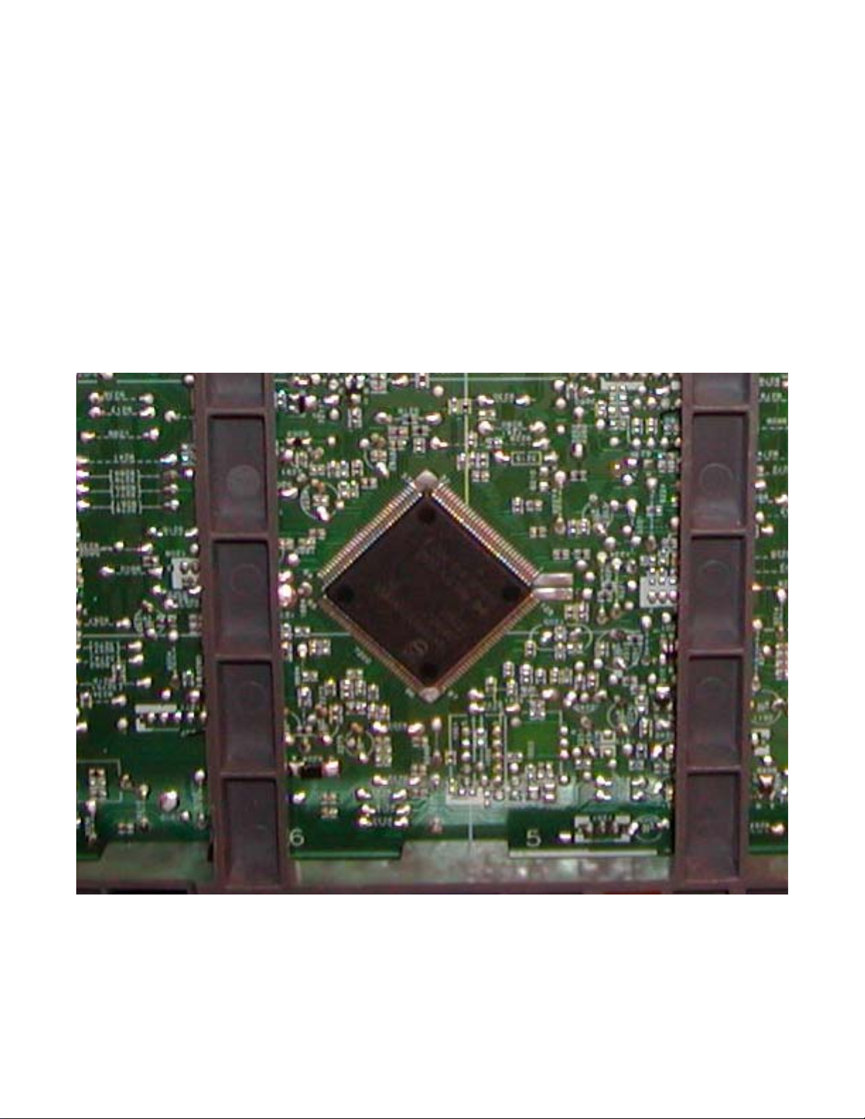
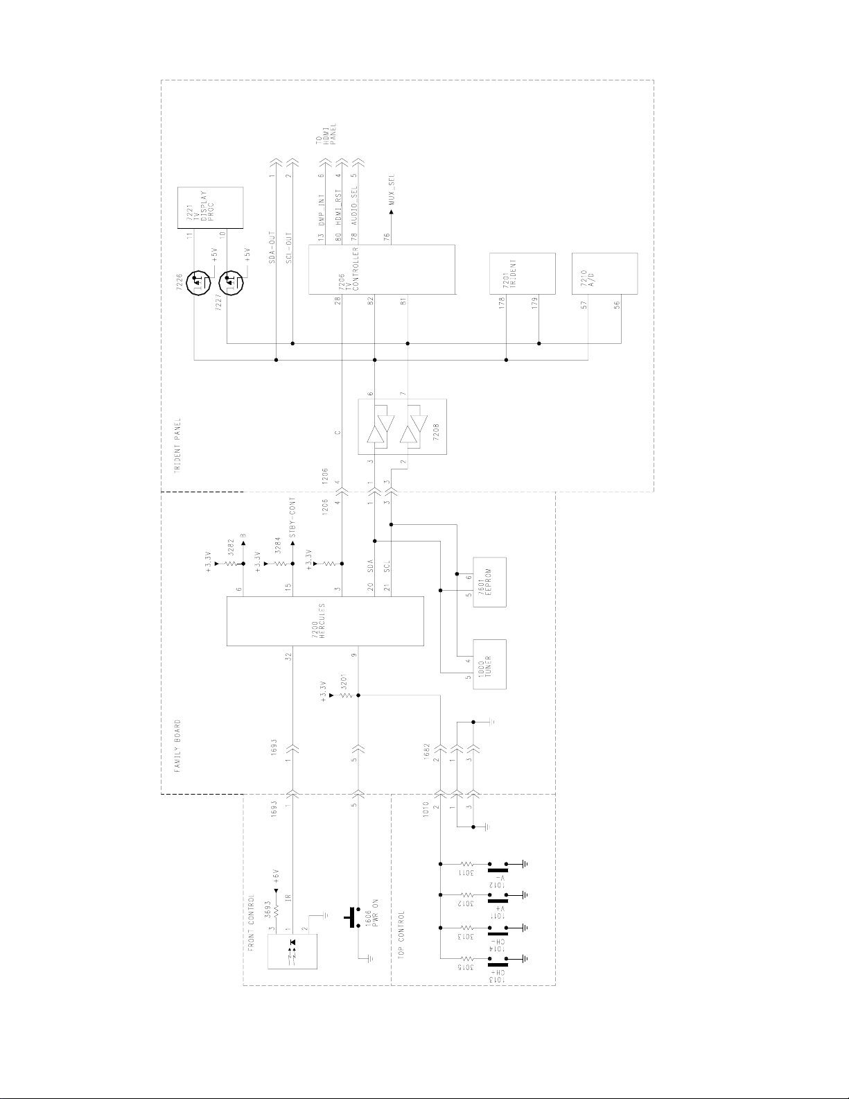
The L05HD has two microprocessors, The Hercules located on the Family board and the TV
Controller located on the Trident board.
The Hercules, 7200, provides control for the entire set. During standby, the Hercules and the
Remote sensor are powered by the 3.3 volt supply. The customer communicates with the
Hercules via the Remote sensor and Power switch located on the Front Control panel. The
power supplies are switched On via the STBY-CONT and B lines. The TV Controller is reset
by the C control line. The I2C bus communicates with the EEPROM 7601, Tuner 1000, TV
Controller 7206, Trident 7201, A/D 7210, TV Display Processor, 7221, and HDMI panel.
HERCULES PROCESSOR
Page 13
Page 16
Page 14
FIGURE 7 - CONTROL
Page 17
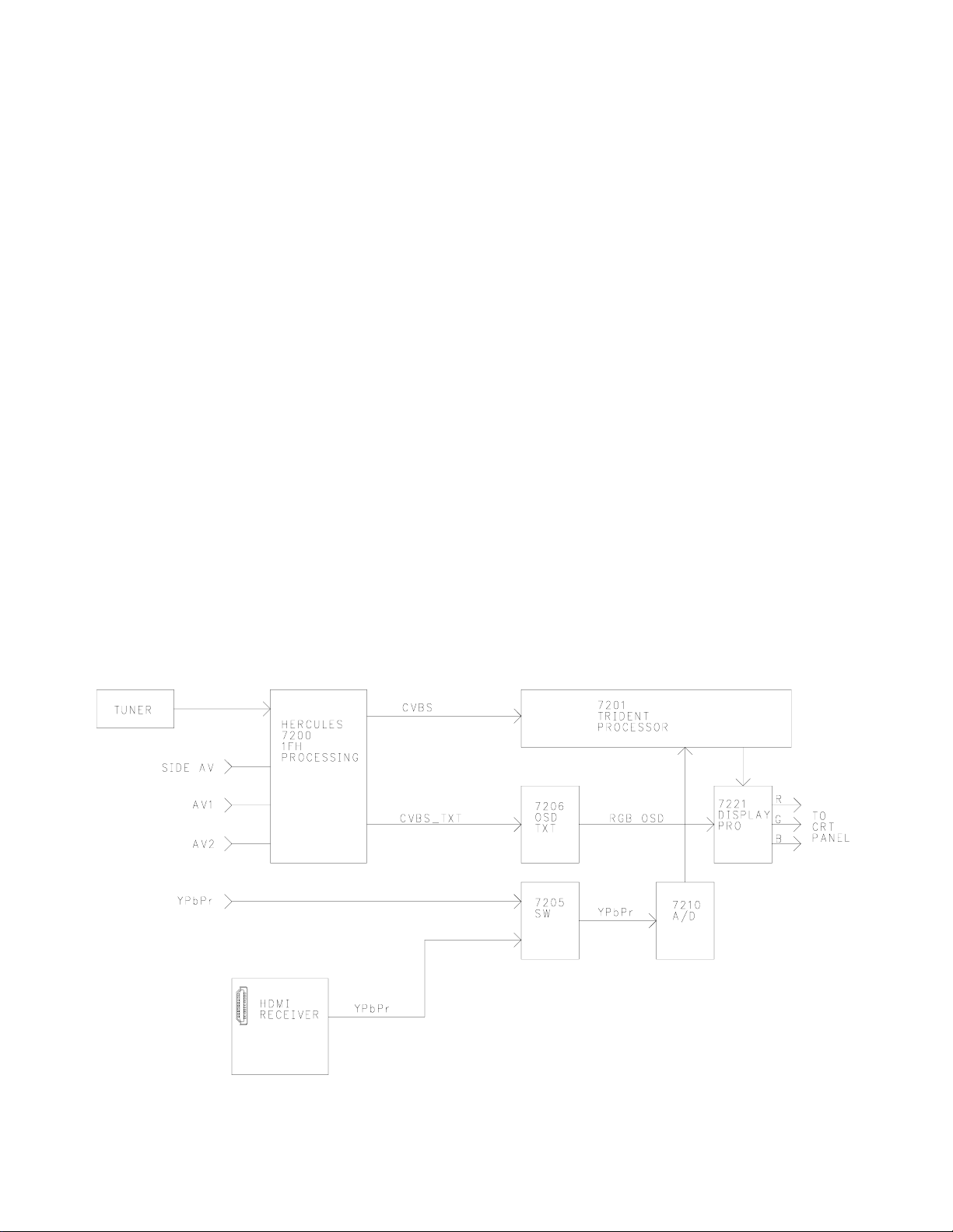
Video Signal flow overview (Figure 8)
There are two sections in the set for processing video. The 1fH section using the Hercules
processes NTSC signals.
The Tuner is controlled by the microprocessor in the Hercules. IF from the Tuner is fed to the
Hercules chip for detection and demodulation. AV1, AV2, Side, and 1fH Component video is
also fed to the Hercules, IC 7200. If an NTSC signal is selected by the Remote or Keyboard,
the selected CVBS (Composite Video) is output on two lines. One CVBS line goes to the
Trident chip, IC 7201, located on the HD panel. CVBS_TXT is fed to IC 7206 on the HD
panel which detects Closed Caption text or teletext. This IC also generates the OSD (On
Screen Display).
If the signal applied to the set is a 2fH signal or better, it is applied to either the YpbPr
Component input or the HDMI input. These signals are fed to a selector switch located on
the HD panel, IC 7205. The selected component or RGB signal if fed to the A/D converter, IC
7210. This signal is fed to the Trident IC 7201 which enhances the picture and scales it to
1080i. Analog RGB out from the Trident IC is fed to the Display Processor, IC 7221, which
performs the picture control functions and inserts the OSD. The output of 7221 is fed to the
CRT panel.
The option settings for the Source selection can be found in Option settings in the SAM
mode.
FIGURE 8 - VIDEO SIGNAL FLOW BLOCK
Page 15
Page 18

AV1, AV2, CVI (480i), Side, and Tuner selections are made by the Hercules chip. Selected
CVBS (Composite Video) from one of these inputs is fed to the Trident panel which selects
between the output of the Hercules, CVI (480p, 720p, 1080i), and the HDMI panel. The CVI
input is shared by the Hercules and the HD section.
The L05HD has the following inputs in addition to the tuner RF:
· AV1 is a Composite video input.
· CVI (Component Video input) can accept 480i, 480p, 720p, or 1080i.
· AV2 accepts Composite video (CVBS) or S-Video.
· Side accepts Composite video (CVBS) or S-Video.
· HDMI (High Definition Multimedia Interface) accepts 480p, 720p, or 1080i video and
audio in a digital TMDS format.
Detailed Signal flow (Figure 9)
The output of the Tuner is fed to the SAW filter, 1002, and then to 7200, Hercules, on Pins
104 and 105. The SVHS (YC) signals are combined inside 7200. IC 7200 selects between
AV1, AV2, Side, and Tuner composite video. The selected composite video is output on Pin
65. Video buffered by Transistor 7211 is fed to IC 7206 located on the Trident panel which
extracts Closed Caption text and Teletext information. This IC also generates the OSD (On
Screen Display). Video buffered by 7212 is fed to the Trident IC which has an internal 3-D
Comb Filter and A/D converter. IC 7201 rescales the picture to 1080i.
Component video is inserted into the YPbPr input located on the Family board. The HDMI
panel converts the HDMI signal into an analog YPbPr format. Both of these signals are fed to
the Switch, 7205 which selects between the two. The selected signal is fed to IC 7210 which
performs an A/D conversion. This 24 bit signal is fed to 7201. The Scaler (Trident IC) converts the signal to a 1080i format as well as performing picture enhancement functions.
DRAM ICs 7215, 7216, 7217, and 7218 stores picture data for the Scaler as it is being
processed. And internal D/A conversion circuit outputs the 1080i signal is an RGB format on
Pins 27, 28 and 29. Horizontal and Vertical sync is output on Pins 34 and 35.
The RGB signal from the Scaler is fed to the TV Display Processor, 7221. RGB is output
from this IC to the CRT panel. Horizontal and Vertical drive is output to the Family board.
TV Display Processor (Refer to Figure 5)
IC 7221 is used in a large number of Philips chassis for a long period of time. RGB in insert-
ed in Pins 30, 31, and 32. This signals are converted to a YUV format before being fed to the
Color level control. RGB from 7206 is inserted on Pins 35, 36, 37, and 38. The signal then
goes to a Brightness and Controls control circuit. RGB to the CRT panel is output on Pins
40, 41, and 42. During warm up, a cathode calibration signal is fed to the CRT panel on the
RGB lines. This signal is then fed back to
Page 16
Page 19
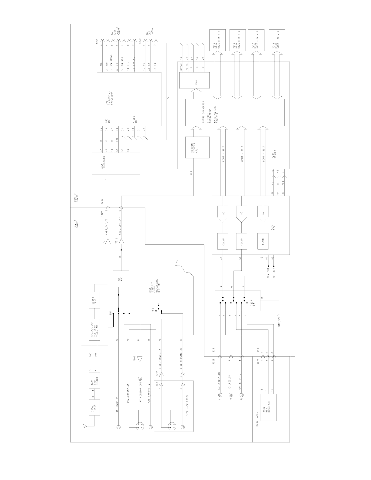
FIGURE 9 - DETAILED VIDEO SIGNAL FLOW BLOCK
Page 17
Page 20
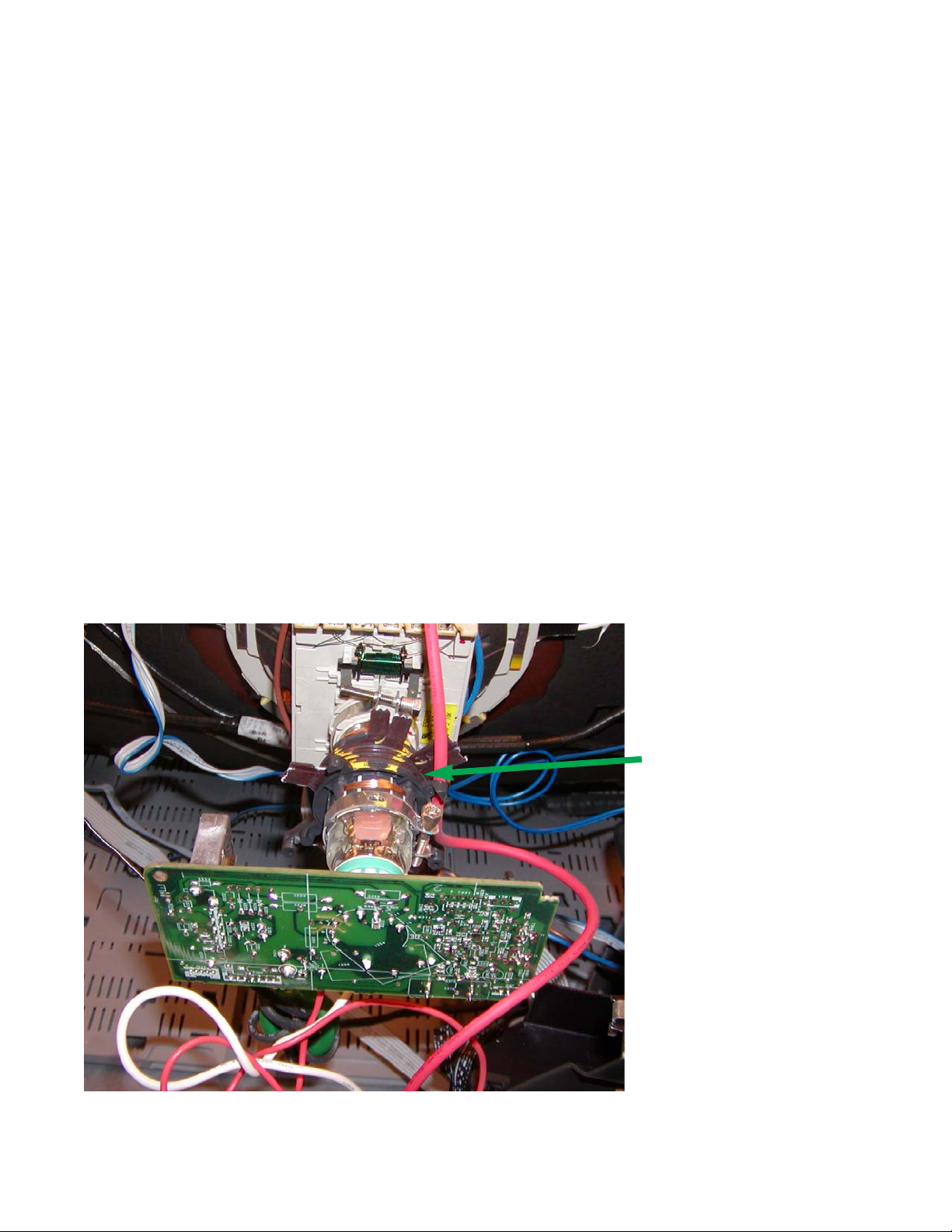
CRT panel (Figure 10)
RGB is fed to the CRT panel on connector 1331. The CRT panel for the L05HD has a single
chip CRT drive circuit. RGB is fed to 7330 on Pins 1, 2, and 3. Signal is output to the CRT
on Pins 7, 8, and 9. BC_INFO or Cutoff on Pin 5 is fed back to the TV Signal Processor on
the Trident panel. The IC is powered by a 200 volt supply on Pin 6.
DC operating voltages for the CRT panel are located on connector 1351. The Filament voltage is located on Pin 2. The 200VA voltage on Pin 5 powers 7330. The VBAT voltage on
Pin 3 and the +12V_LOT voltage on Pin 6 powers the SVM circuit.
SVM (Figure 11)
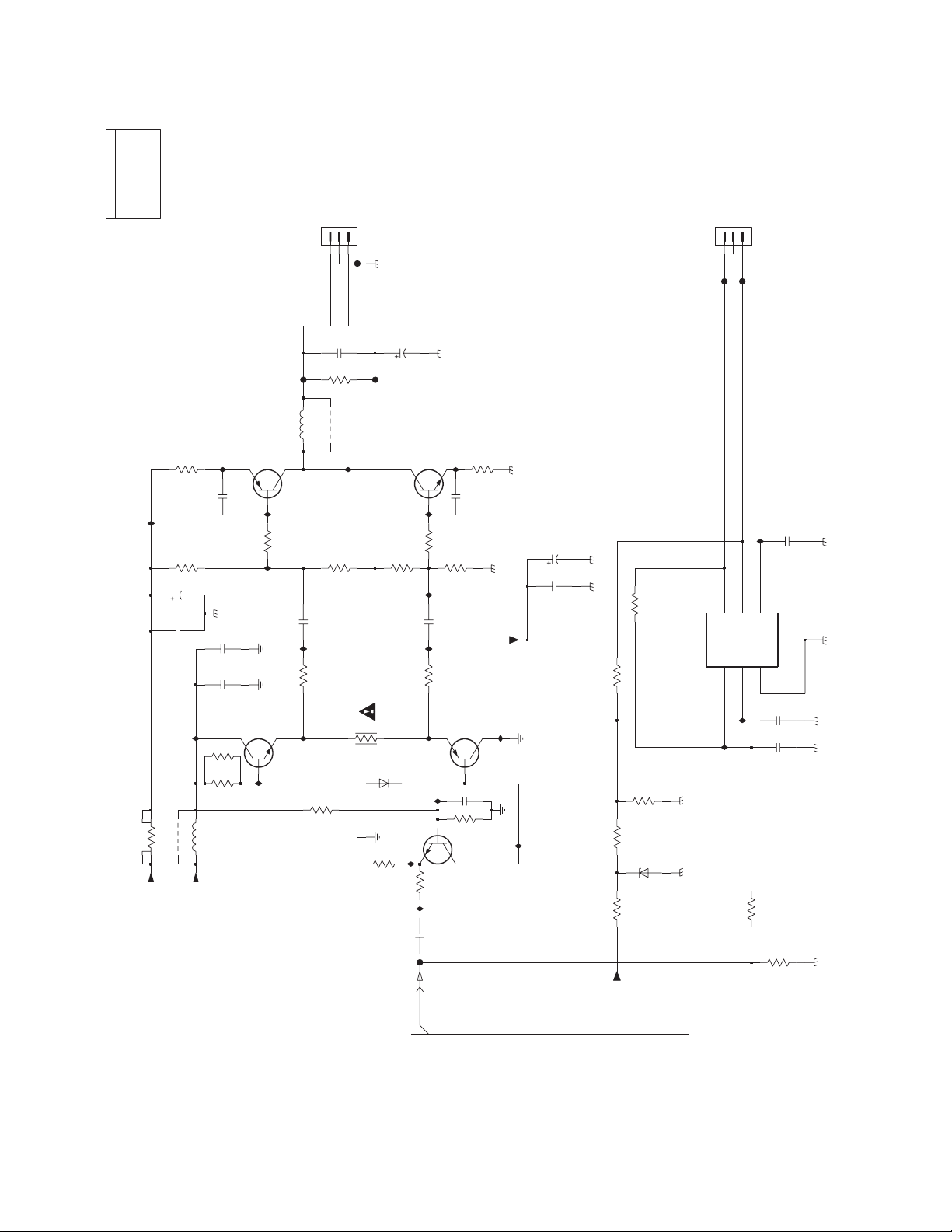
There are two coils on the deflection coil in addition to the Vertical and Horizontal winding.
The SCAVEM coil (Scan Velocity Modulation) sharpens the edges between light and dark
transitions.
The SVM_ROT signal drives both the SCAVEM and the Rotation coil. The SCAVEM circuit is
powered by the Vbatt and +12V_LOT supplies. Capacitor 2376 blocks the dc Rotation signal
to prevent it from entering the SCAVEM circuit. Capacitor 2381 blocks the higher frequency
SCAVEM signal to prevent it from affecting the Rotation drive.
Page 18
SVM Coil
Page 21
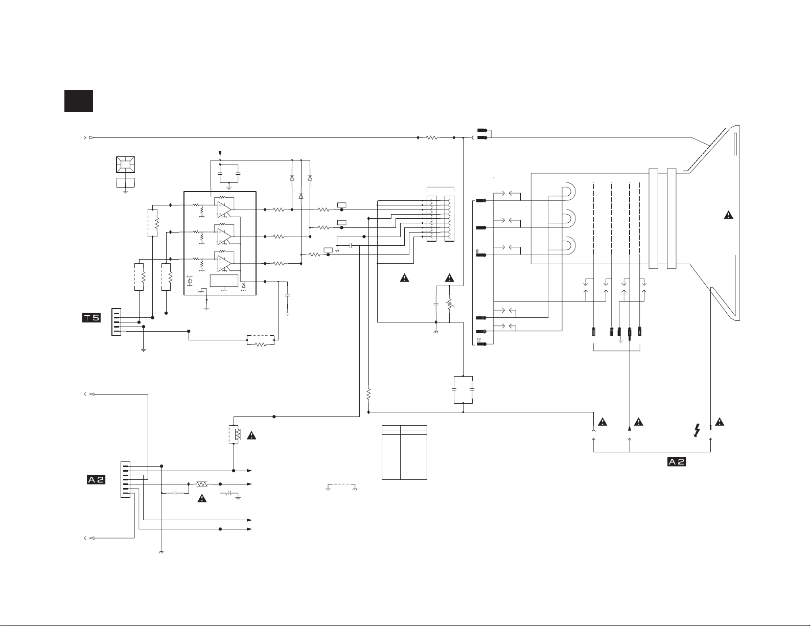
Blue
Green
Red
7V
THERMAL
PROTECTION
IN1
IN2
IN3
GND
BC1
OUT3
OUT2
OUT1
3k77
3k77
3k77
3k75
3k75
3k75
188k7
188k7
188k7
Vdd
Vdd
Vdd
Vref
Vref
Vref
Vref
2.5V
BC1
BC2
BC3
A1
A2
A3
From 1202 of
5
R
AQUADAG
WIRE
2V5
VG2
10n
***
B
2V5
*
I357
I355
6V
156V
FROM LOT, MAIN CHASSIS
1n5
CRT
V
2V5
156V
156V
CRT Sockets
*
7
NOT USED
G
CRT PANEL
Line + Frame
200V
**
**
47n
FOCUS
1
T0 CRT SOCKET
EHT
From 1401 of
T0 CRT SOCKET
of Trident Panel
Deflection
LINE + FRAME DEFLECTION
*
3357
F351
F356
D?
TYPE
6332
BAV21
I337
2330
100n
3334
1K0
F339
4334
2334
I339
F334
I332
3n3
2353
4330
680p
2352
3329
100R
4329
F340
I333
I335
I331
1K0
3332
100R
3328
F354
F338
I334
I336
6331
BAV21
100R
3335
3333
100R
1332
I330
I351
2350
2333
1n0
9360
F335
HEATSINK
0330
2331
10n
F332
4328
1K0
3336
3337
F353
F352
3330
100R
2351
10u
3354
1K5
2332
F341
100R
3360
1352
BAV21
6333
I340
F333
I338
9337
I353
7
100R
3331
1
2
3
4
5
6
1351
8
9
I352
F331
1
10
11
12
5
6
7
8
9
1254
10
11
12
5
6
7
1256
1
3351
100R
3
4
5
7330
1
2
3
4
5
6
7
8
9
1331
1
2
10R
3356
GND_CRT
Filament
+12V_LOT
+200VA
BC_INFO
EHTinfo
+200VA
EHTinfo
Vbatt
SVM_ROT
B1
REGION
SET
NAFTA
27VRF-HD
3328
3329
3330
3337
3360
4328
4329
---
---
---
---
--JMP
JMP
4330
9337
JMP
---
9360 JMP
FIGURE 10 - CRT PANEL
Page 19
Page 22
0V5
1R8
TO
7V8
B
8K2
47V3
C
7V5
*
*
*
96V
E
7V5
2V3
B
E
2SC3421
C
E
C
B
1V7
7V2
0V
TO
*
97V3
ROTATION COIL
*
*
E
B
E
*
B
C
E
3V8
6V7
8V2
10V8
6V8
12V8
SCAVEM COIL
7V2
47V2
B1
22n
*
2SA1358
*
3367
I365
9361
3373
16V10u
2390
2391
100n
400V
2364
4n7
3389
33R
F382
3382
6K8
4n7
UDZS-6V8
2365
6381
I363
7362
BC857B
BC847B
7376
F381
I367
I364
2385
2389
2368
1u0
5331
10R
3362
150K
3390
150K
3391
680K
3393
22K
3392
F362
3387
2362
1n0
10n
2387
BC847B
7361
F363
I348
8K2
3372
I380
I361
3365
10R
I366
3368
820R
330R
3376
5361
F361
+12V_LOT
4
MODE
2
OUT+
7
OUT-
SVR
6
1
VCC
7364
TDA8941P
8
GND
3
IN+5IN-
1381
123
7331
1K8
3375
I344
I345
I342
I343
I341
2383
100n
33R
3388
3363
820R
3369
10R
2367
10u 100V
220R
3377
2361
47n 250V
3371
470R
I371
22u
2363
3366
68K
F360
100V
2376
100n
I347
3361
680R
1R8
3364
1361
123
I362
I346
4331
2381
100n
68K
1N4148
6361
3370
I372
2384
100n
2382
7363
6K8
3381
I360
3394
6K8
+12V_LOT
I369
I381
I368
Vbatt
+12V_LOT
SVM_ROT
REGION
SET
NAFTA
27VRF-HD
4331
5331
5361
9361
--1U0 PM10
100MHZ 50R
---
Page 20
FIGURE 11 - SVM AND ROTATION
Page 23
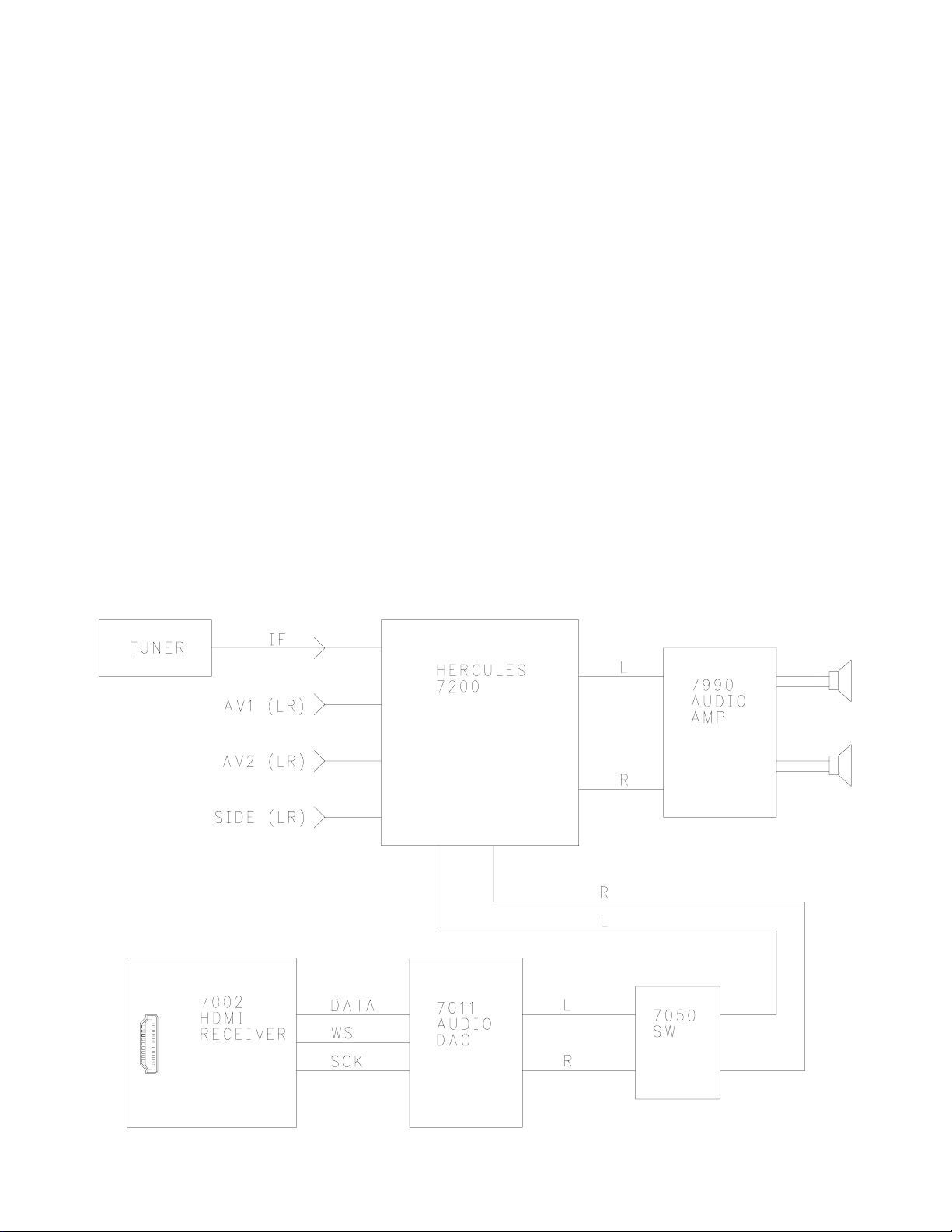
Audio (Figure 12)
All audio processing and control is performed by the Hercules IC 7200 located on the main
board.
Audio is included in the HDMI bit-stream. Digital audio from 7002 is fed to IC 7011, Audio
DAC. Audio from 7011 is fed to IC 7050, switch, which has only one input since the second
input is not used in the HD version. The output of 7050 is fed to the Hercules IC located on
the Main board. Audio for the CVI input should be inserted into AV1. Audio is output from the
Hercules on Pins 68 and 69 to the Audio Amplifier, IC 7990. This is a two channel 20 watt
amplifier.
Audio output
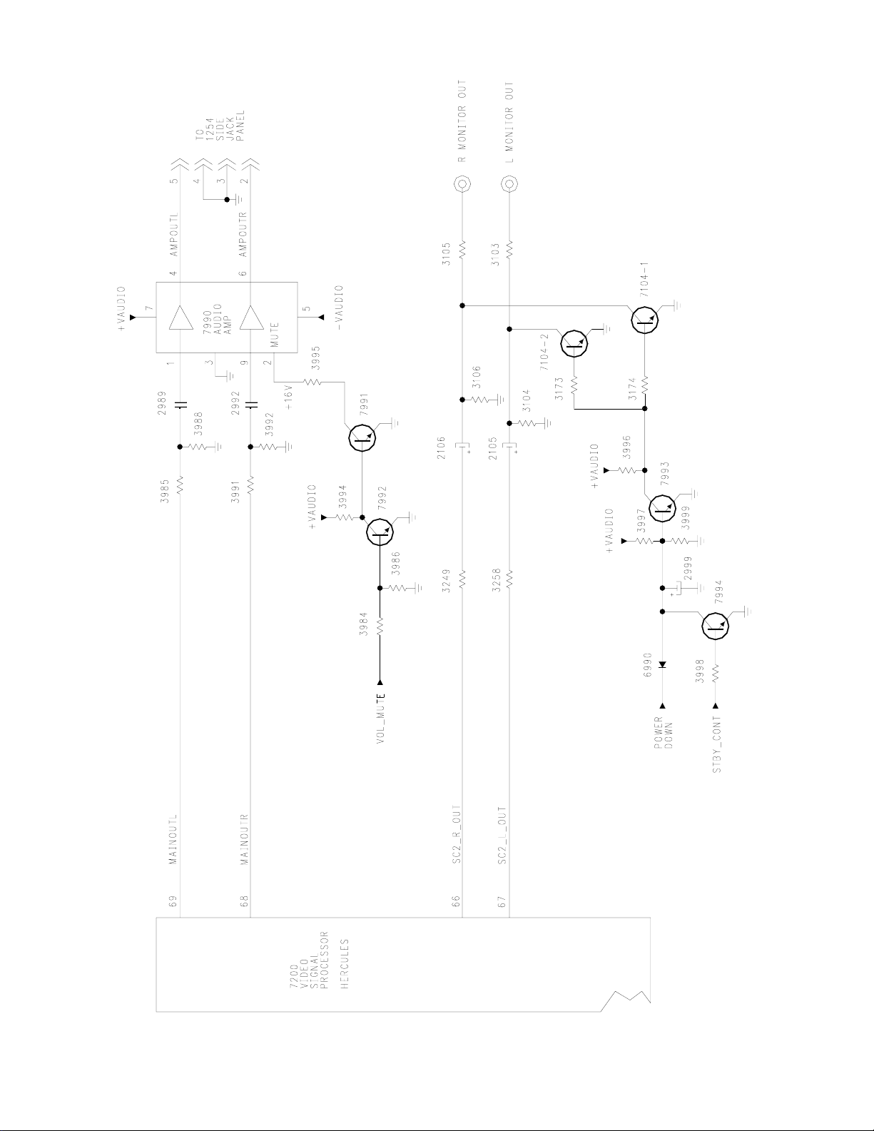
Main audio is output on Pins 68 and 69 and fed to the audio amplifier 7990. The audio ampli-
fier is a dual 10 watt amplifier. It is powered by the +VAUDIO and -VAUDIO supplies. These
are +16 and -16 volts. To mute the amplifier, the VOL_MUTE line goes Low switching transistor 7992 Off switching transistor 7991 On. The output of the amplifier is fed to the Side
Jack panel.
Monitor audio is output on Pins 66 and 67 of 7200. These outputs are muted by the
STBY_CONT and POWER DOWN lines. The POWER DOWN line is High during normal
operation. As the set powers off, this line goes Low, switching 7993 Off. Transistor 7104
then switches On to mute the output. The STBY_CONT line goes High when the set is
FIGURE 12 - AUDIO BLOCK
Page 21
Page 24
Page 22
FIGURE 13 - AUDIO OUTPUT
Page 25
*
*
470pF
470pF
HEADPHONE
ECO SUB
TO
TO
SPEAKERS
I166
I168
3157
1
2
3
1279
6
7
8
9
1232
1
2
3
4
5
I162
I163
2181
1u
I170
I169
I171
39K
3161
1
2
3
4
5
1254
2176 2178
F154
3156
1278
1
2
3
4
FIGURE 14 - SIDE JACK PANEL
turned Off turning 7994 On, muting the output. Capacitor 2999 delays the turn-on of 7993 to
prevent a pop in the speaker at set turn On.
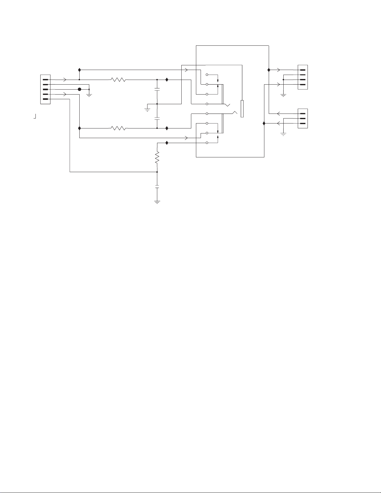
Side Jack panel (Figure 14)
The output of the audio amplifier is fed to the Headphone Jack located on the Side Jack
panel. The output to the speakers is switched Off when a headphone plug is inserted.
Finding the defective panel (Figures 15 and 16)
When troubleshooting the set, the defective panel requiring replacement or additional repair
must be located. The Power supplies, Deflection, 1fH inputs, and Audio outputs are located
on the Family board. The 2fH, CRT drive, and Deflection drive circuits are located on the
Trident board.
If the set turns On without a picture or sound, first check the power supplies located on the
Family board. If the set comes On, then shuts Off, there may be a problem with the shutdown circuits which are located on the Family board. If the picture is missing, but sound and
high voltage are present, the problem may be located on the Trident panel.
Page 23
Page 26
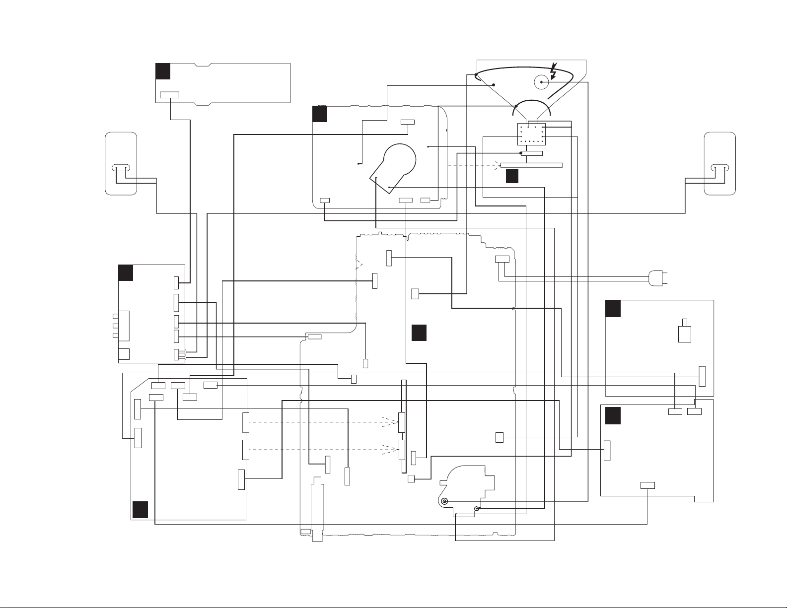
Wiring Diagram
SIDE
A/V PANEL +
HEADPHONE
D
CRT PANEL
(component view)
B
TOP CONTROL PANEL
E
A
HEADPHONE
RIGHT (RED)
LEFT (WHITE)
CVBS (YELLOW)
1010
CRT PANEL
B
MONO
CARRIER
3P
RED
BLACK
RIGHT
SPEAKER
BLACK
RED
LEFT
SPEAKER
GREY
ORANGE
EHT
CRT
FRAME
ROTATION
COIL
AQUADAG
DEGAUSSING COIL
SCAVEM
COIL
CRT
16:9
1211
1693
FRONT INTERFACE
J
MAINS
CORD
MAINS
SWITCH
2P
7P
Warning: Some models have tact switch.
5P
5P
7P
1693
7P
1207
1005
7P
1252
2P
1451
3P
1682
2P
1401
5P
1254
3P
1280
4P
1278
1280
5P
1351
3P
1361
3P
1381
1504
LOT
TUNER
1223
HDMI PANEL
M
4P
1352
1335
CRT
SOCKET
3P
COMPAIR
CONNECTOR
TRIDENT PANEL
T
1223
4P
1250
12P
1251
10P
1202
5P
1250
12P
1251
10P
5P
1340
1206
4P
1533
12P
1221
6P
1220
7P
1228
6P
1222
6P
1222
6P
1221
6P
1220
7P
6P
1228
4P
1206
12P
1533
3P
1281
1336
2P
1404
BLUE
BROWN
Page 24
FIGURE 15 - CONNECTOR INTERCONNECT
Page 27
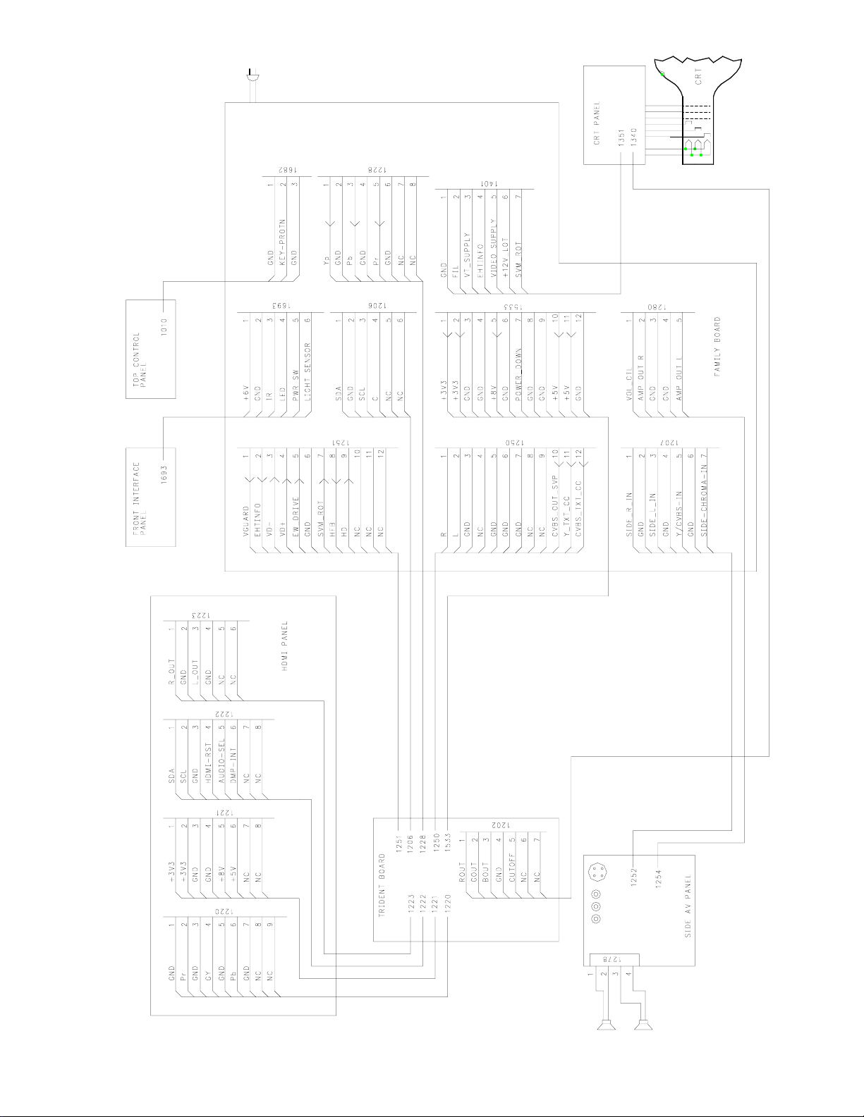
FIGURE 16 - WIRING INTERCONNECT
Page 25
Page 28
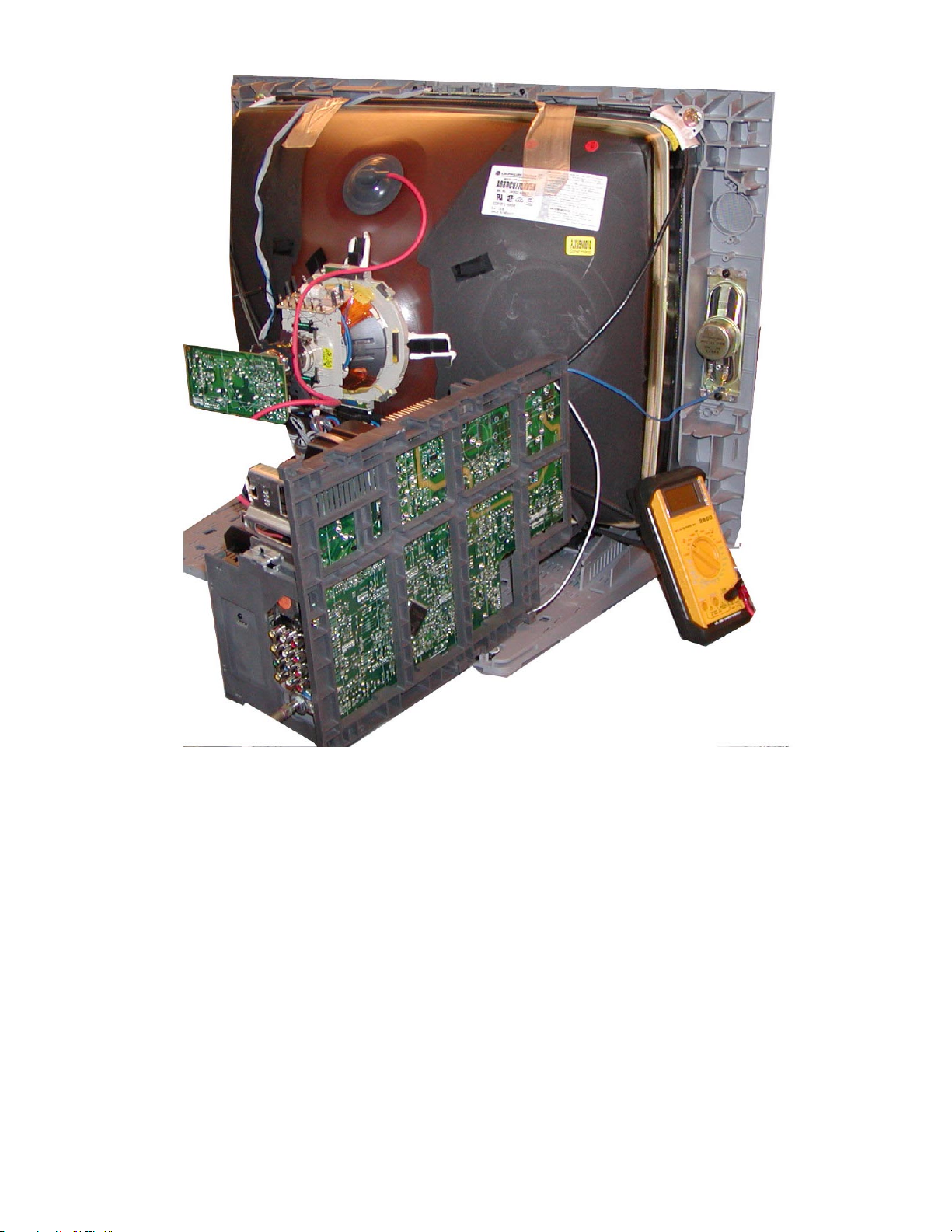
Page 26
SERVICE POSITION
Page 29
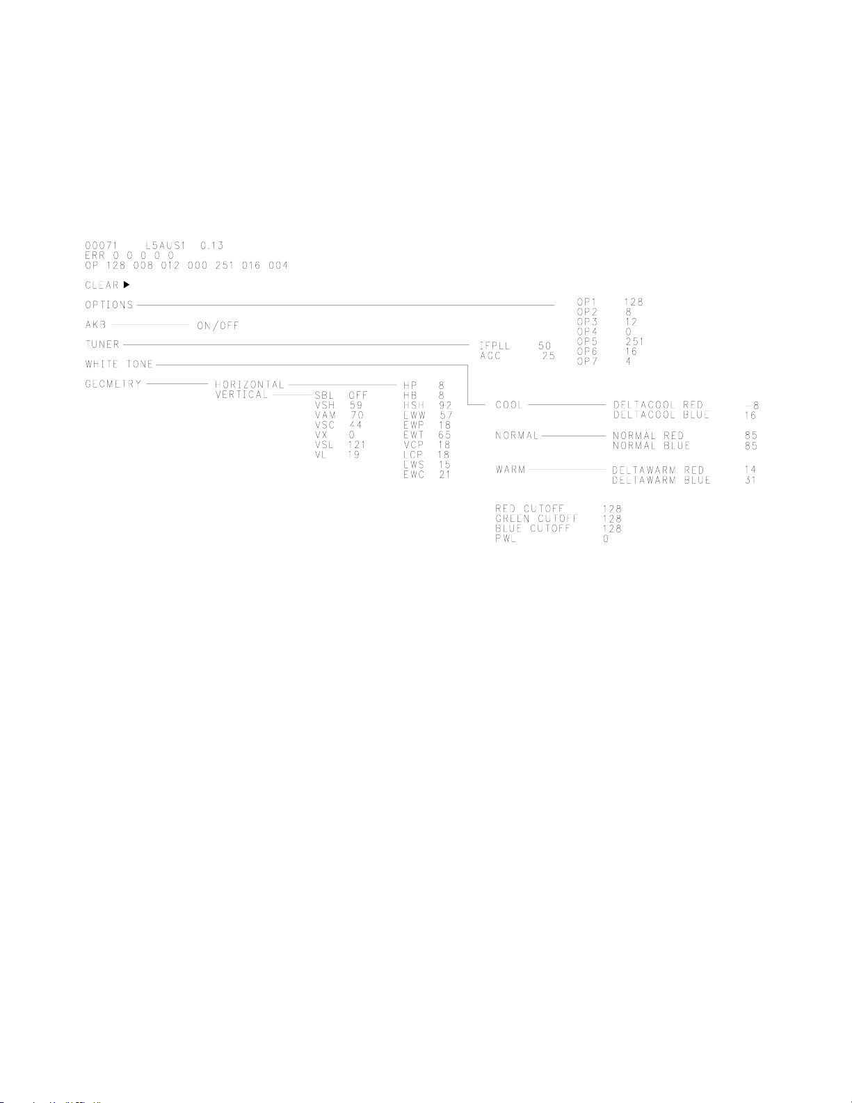
Service Alignment Mode SAM (Figure 17)
Making changes in the settings requires entering the SAM. To enter SAM, press 0 6 2 5 9 6
Info on the remote control. Use the cursor-up and cursor-down buttons to highlight a selection. Press the cursor-right, cursor-left buttons, or enter a value to make changes. Refer to
the Service manual for additional information on the SAM.
FIGURE 17 - SERVICE ALIGNMENT MODE
Page 27
Page 30

Abbreviation list
Description
1080i 1080 visible lines, interlaced
1080p 1080 visible lines, progressive scan
480i 480 visible lines, interlaced
480p 480 visible lines, progressive scan
ADC A/D Analogue to Digital Converter
AFC Automatic Frequency Control: control signal used to tune to the correct
frequency
AGC Automatic Gain Control: algorithm that controls the video input of the
feature box
AM Amplitude Modulation
AV Audio Video
C-FRONT Chrominance front input
CBA Circuit Board Assembly (or PWB)
ComPair Computer aided rePair
CSM Customer Service Mode
CVBS Composite Video Blanking and Synchronization
CVBS-EXT CVBS signal from external source (VCR, VCD, etc.)
CVBS-INT CVBS signal from Tuner
CVBS-MON CVBS monitor signal
CVBS-TER-OUT CVBS terrestrial out
DAC Digital to Analogue Converter
DFU Directions For Use: owner's manual
DNR Dynamic Noise Reduction
DRAM Dynamic RAM
DSP Digital Signal Processing
DTS Digital Theatre Sound
DVD Digital Video Disc
EEPROM Electrically Erasable and Programmable Read Only Memory
EPLD Electronic Programmable Device
EXT EXTernal (source), entering the set by cinches (jacks)
FBL Fast Blanking: DC signal accompanying RGB signals
FLASH FLASH memory
FM Field Memory / Frequency Modulation
FMR FM Radio
FRC Frame Rate Converter
FRONT-C Front input chrominance (SVHS)
FRONT-DETECT Front input detection
FRONT-Y_CVBS Front input luminance or CVBS (SVHS)
H H_sync to the module
HD High Definition
HDMI High Definition Multimedia Interface
HP HeadPhone
I2C Integrated IC bus
I2S Integrated IC Sound bus
Page 28
Page 31

IC Integrated Circuit
IF Intermediate Frequency
Interlaced Scan mode where two fields are used to form one frame. Each field contains
half the number of the total amount of lines. The fields are written in 'pairs',
causing line flicker.
IR Infra Red
IRQ Interrupt ReQuest
Last Status The settings last chosen by the customer and read and stored in RAM or in the
NVM. They are called at start-up of the set to configure it according the cus-
tomers wishes
LCD Liquid Crystal Display
LED Light Emitting Diode
LINE-DRIVE Line drive signal
LVDS Low Voltage Differential Signalling, data transmission system for high speed
and low EMI communication.
MPEG Motion Pictures Experts Group
NVM Non Volatile Memory: IC containing TV related data (for example, options)
OSD On Screen Display
Progressive Scan Scan mode where all scan lines are displayed in one frame at the same
time, creating a double vertical resolution.
RAM Random Access Memory
RC Remote Control transmitter
RC5 Remote Control system 5, the signal from the remote control receiver
RGB Red, Green, and Blue. The primary colour signals for TV. By mixing
levels of R, G, and B, all colors (Y/C) are reproduced.
RGBHV Red, Green, Blue, Horizontal sync, and Vertical sync
ROM Read Only Memory
SAM Service Alignment Mode
SIF Sound Intermediate Frequency
SC SandCastle: two-level pulse derived from sync signals
SCL CLock Signal on I2C bus
SDA DAta Signal on I2C bus
SDRAM Synchronous DRAM
SIF Sound Intermediate Frequency
STBY STandBY
VGA Video Graphics Array
XTAL Quartz crystal
YPbPr Component video (Y= Luminance, Pb/Pr= Colour difference signals)
Y/C Luminance (Y) and Chrominance (C) signal
Y-OUT Luminance-signal
Page 29
Page 32

 Loading...