

Page 1
Colour Television Chassis
L03.2L
AA
E_14560_000.eps
260204
Contents Page
1. Technical Specifications, Connections and Chassis Overview 2
2. Safety Instructions, Warnings, and Notes 4
3. Directions for Use 5
4. Mechanical Instructions 6
5. Service Modes, Error Codes, and Fault Finding 7
6. Block Diagrams, Testpoint Overviews, and Waveforms
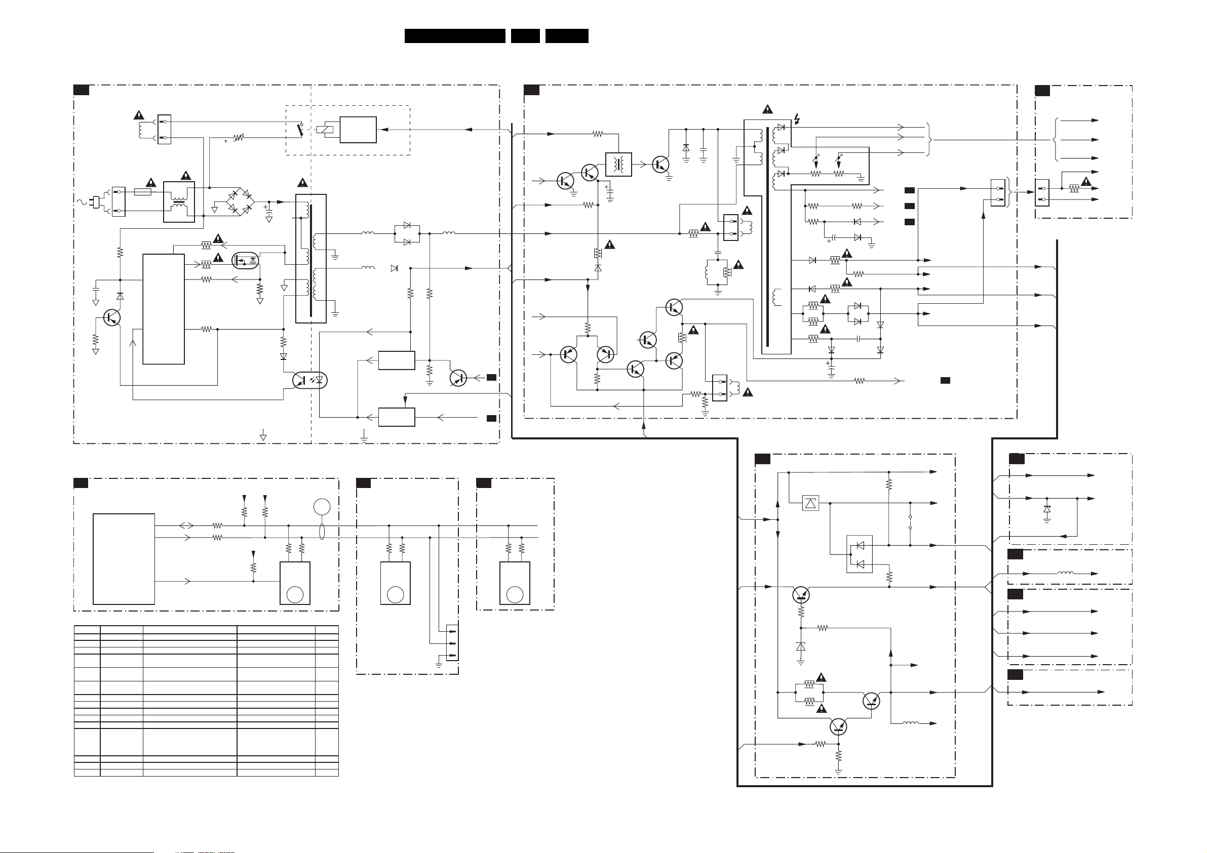
Block Diagram 11
I2C and Supply Voltage Overview 12
Testpoint Overview Mono Carrier and CRT Panel 13
7. Circuit Diagrams and PWB Layouts Diagram PWB
Mono Carrier: Power Supply (A1)14 21-24
Mono Carrier: Deflection (A2)15 21-24
Mono Carrier: Tuner IF (A3)16 21-24
Mono Carrier: Video Processing (A4)17 21-24
Mono Carrier: Audio - BTSC Stereo Decoder (A5)18 21-24
Mono Carrier: Audio Amplifier + Mono Sound Processing (A6)19 21-24
Mono Carrier: Front I/O + Front Control + Headphone (A7)20 21-24
CRT Panel (B1)25 26
8. Alignments 27
9. Circuit Descriptions, List of Abbreviations, and IC Data Sheets34
Abbreviation List 37
10. Spare Parts List 39
11. Revision List 42
©
Copyright 2005 Philips Consumer Electronics B.V. Eindhoven, The Netherlands.
All rights reserved. No part of this publication may be reproduced, stored in a
retrieval system or transmitted, in any form or by any means, electronic,
mechanical, photocopying, or otherwise without the prior permission of Philips.
Published by JH 0564 TV Service Printed in the Netherlands Subject to modification EN 3122 785 15381
Page 2
EN 2 L03.2L AA1.
Technical Specifications, Connections and Chassis Overview
1. Technical Specifications, Connections and Chassis Overview
Index of this chapter:
1.1 Technical Specifications
1.2 Connection Overview
1.3 Chassis Overview
Note: Figures below can deviate slightly from the actual
situation, due to the different set executions.
1.1 Technical Specifications
1.1.1 Vision
Display type : CRT, DV, FSQ
Screen size : 14” (37 cm), 4:3
: 21” (55 cm), 4:3
Tuning system : PLL
TV Colour systems : NTSC M/N 3.58
Video playback : NTSC M/N 3.58, 4.43
Channel selections : 181 presets
1.1.2 Sound
Sound systems : FM-mono
Maximum power (W
) : 1 x 1 (3005-models)
RMS
: PAL B/G
: Full-Cable
(3005-models)
: BTSC with SAP
(3205-models)
: 2 x 1 (3205-models)
Mini Jack: Audio Head phone - Out
Bk - Head phone 8 - 600 ohm / <4 mW ot
Cinch: Video CVBS - In, Audio - In
Ye -Video CVBS 1 V
Wh - Audio L 0.2 V
Rd - Audio R 0.2 V
/ 75 ohm jq
PP
/ 10 kohm jq
RMS
/ 10 kohm jq
RMS
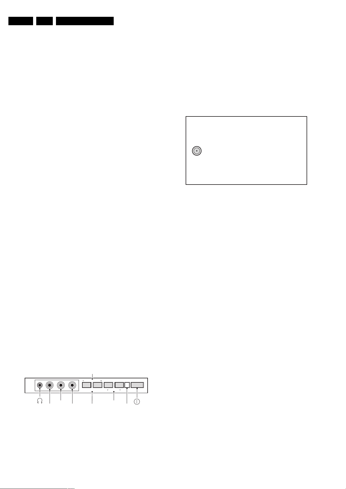
1.2.2 Rear Connections
75 Ohm ANT.
Figure 1-2 Rear connections
FM Ant
1 -F type 75 ohm, coax D
E_14560_015.eps
260204
1.1.3 Miscellaneous
Power supply:
- Mains voltage (V
) : 220-240 (/44 models)
AC
: 105-132 (/55 models)
- Mains frequency (Hz) : 50 / 60
Ambient conditions:
- Temperature range (°C) : +5 to +40
- Maximum humidity : 90% R.H.
1.2 Connection Overview
Note: The following connector colour abbreviations are used
(acc. to DIN/IEC 757): Bk= Black, Bu= Blue, Gn= Green, Gy=
Grey, Rd= Red, Wh= White, and Ye= Yellow.
1.2.1 Front Connections
INSTALL/MENU
INSTALL MENU POWER
- VOLUME + CHANNEL
AUDIO L
AUDIO R
- VOLUME +
CHANNEL
IR LEDVIDEO
E_14560_014.eps
220304
Figure 1-1 Front connections
Page 3
Technical Specifications, Connections and Chassis Overview
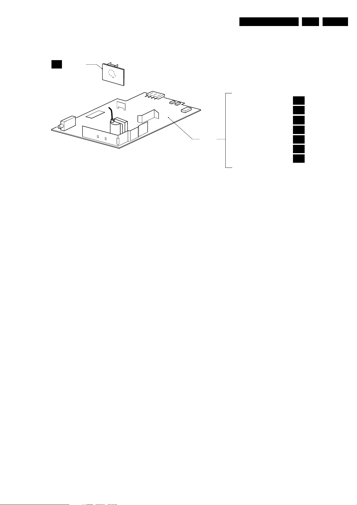
1.3 Chassis Overview
CRT PANEL
B1
EN 3L03.2L AA 1.
MONO
CARRIER
Figure 1-3 Chassis overview
POWER SUPPLY
DEFLECTION
TUNER IF
IF, VIDEO PROCESSING, CONTROL,
AND SYNC.
AUDIO BTSC STEREO DECODER
AUDIO AMP + MONO SOUND PROC.
FRONT I/O + FRONT CONTROL
+ HEADPHONE
E_14560_013.eps
A1
A2
A3
A4
A5
A6
A7
240304
Page 4
EN 4 L03.2L AA2.
Safety Instructions, Warnings, and Notes
2. Safety Instructions, Warnings, and Notes
Index of this chapter:
2.1 Safety Instructions
2.2 Maintenance Instructions
2.3 Warnings
2.4 Notes
2.1 Safety Instructions
Safety regulations require that during a repair:
• Connect the set to the Mains (AC Power) via an isolation
transformer (> 800 VA).
• Replace safety components, indicated by the symbol h,
only by components identical to the original ones. Any
other component substitution (other than original type) may
increase risk of fire or electrical shock hazard.
• Wear safety goggles when you replace the CRT.
Safety regulations require that after a repair, the set must be
returned in its original condition. Pay in particular attention to
the following points:
• General repair instruction: as a strict precaution, we advise
you to re-solder the solder connections through which the
horizontal deflection current is flowing. In particular this is
valid for the:
1. Pins of the line output transformer (LOT).
2. Fly-back capacitor(s).
3. S-correction capacitor(s).
4. Line output transistor.
5. Pins of the connector with wires to the deflection coil.
6. Other components through which the deflection current
flows.
Note: This re-soldering is advised to prevent bad connections
due to metal fatigue in solder connections, and is therefore only
necessary for television sets more than two years old.
• Route the wire trees and EHT cable correctly and secure
them with the mounted cable clamps.
• Check the insulation of the Mains (AC Power) lead for
external damage.
• Check the strain relief of the mains (AC Power) cord for
proper function, to prevent the cord from touching the CRT,
hot components, or heat sinks.
• Check the electrical DC resistance between the Mains (AC
Power) plug and the secondary side (only for sets which
have a Mains (AC Power) isolated power supply):
1. Unplug the Mains (AC Power) cord and connect a wire
between the two pins of the Mains (AC Power) plug.
2. Set the Mains (AC Power) switch to the "on" position
(keep the Mains (AC Power) cord unplugged!).
3. Measure the resistance value between the pins of the
Mains (AC Power) plug and the metal shielding of the
tuner or the aerial connection on the set. The reading
should be between 4.5 Mohm and 12 Mohm.
4. Switch "off" the set, and remove the wire between the
two pins of the Mains (AC Power) plug.
• Check the cabinet for defects, to avoid touching of any
inner parts by the customer.
2.2 Maintenance Instructions
We recommend a maintenance inspection carried out by
qualified service personnel. The interval depends on the usage
conditions:
• When a customer uses the set under normal
circumstances, for example in a living room, the
recommended interval is three to five years.
• When a customer uses the set in an environment with
higher dust, grease, or moisture levels, for example in a
kitchen, the recommended interval is one year.
• The maintenance inspection includes the following actions:
1. Perform the “general repair instruction” noted above.
2. Clean the power supply and deflection circuitry on the
chassis.
3. Clean the picture tube panel and the neck of the picture
tube.
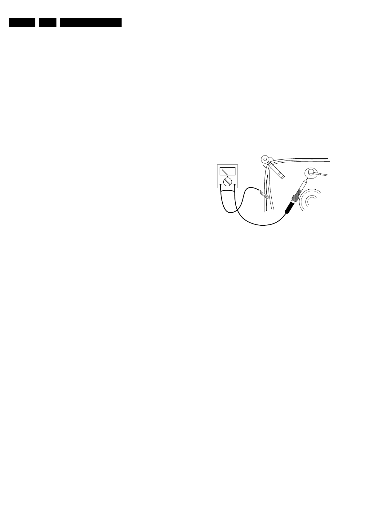
2.3 Warnings
• In order to prevent damage to ICs and transistors, avoid all
high voltage flashovers. In order to prevent damage to the
picture tube, use the method shown in figure “Discharge
picture tube”, to discharge the picture tube. Use a high
voltage probe and a multi-meter (position V
until the meter reading is 0 V (after approx. 30 s).
V
Figure 2-1 Discharge picture tube
• All ICs and many other semiconductors are susceptible to
electrostatic discharges (ESD w). Careless handling
during repair can reduce life drastically. Make sure that,
during repair, you are connected with the same potential as
the mass of the set by a wristband with resistance. Keep
components and tools also at this same potential. Available
ESD protection equipment:
– Complete kit ESD3 (small tablemat, wristband,
connection box, extension cable and earth cable) 4822
310 10671.
– Wristband tester 4822 344 13999.
• Be careful during measurements in the high voltage
section.
• Never replace modules or other components while the unit
is switched "on".
• When you align the set, use plastic rather than metal tools.
This will prevent any short circuits and the danger of a
circuit becoming unstable.
2.4 Notes
2.4.1 General
• Measure the voltages and waveforms with regard to the
chassis (= tuner) ground (H), or hot ground (I), depending
on the tested area of circuitry. The voltages and waveforms
shown in the diagrams are indicative. Measure them in the
Service Default Mode (see chapter 5) with a colour bar
signal and stereo sound (L: 3 kHz, R: 1 kHz unless stated
otherwise) and picture carrier at 475.25 MHz for PAL, or
61.25 MHz for NTSC (channel 3).
• Where necessary, measure the waveforms and voltages
with (D) and without (E) aerial signal. Measure the
voltages in the power supply section both in normal
operation (G) and in stand-by (F). These values are
indicated by means of the appropriate symbols.
• The semiconductors indicated in the circuit diagram and in
the parts lists, are interchangeable per position with the
). Discharge
DC
E_06532_007.eps
250304
Page 5

Directions for Use
EN 5L03.2L AA 3.
semiconductors in the unit, irrespective of the type
indication on these semiconductors.
2.4.2 Schematic Notes
• All resistor values are in ohms and the value multiplier is
often used to indicate the decimal point location (e.g. 2K2
indicates 2.2 kohm).
• Resistor values with no multiplier may be indicated with
either an "E" or an "R" (e.g. 220E or 220R indicates 220
ohm).
• All capacitor values are given in micro-farads (µ= x10
nano-farads (n= x10
• Capacitor values may also use the value multiplier as the
decimal point indication (e.g. 2p2 indicates 2.2 pF).
• An "asterisk" (*) indicates component usage varies. Refer
to the diversity tables for the correct values.
• The correct component values are listed in the Spare Parts
List. Therefore, always check this list when there is any
doubt.
2.4.3 Lead Free Solder
Philips CE is going to produce lead-free sets (PBF) from
1.1.2005 onwards.
-9
), or pico-farads (p= x10
P
b
Figure 2-2 Lead-free logo
This sign normally has a diameter of 6 mm, but if there is less
space on a board also 3 mm is possible. Regardless of this logo
(is not always present), one must treat all sets from this date
onwards according to the following rules
Due to lead-free technology some rules have to be respected
by the workshop during a repair:
• Use only lead-free soldering tin Philips SAC305 with order
code 0622 149 00106. If lead-free solder paste is required,
please contact the manufacturer of your soldering
equipment. In general, use of solder paste within
workshops should be avoided because paste is not easy to
store and to handle.
• Use only adequate solder tools applicable for lead-free
soldering tin. The solder tool must be able
-12
– To reach at least a solder-tip temperature of 400°C.
– To stabilise the adjusted temperature at the solder-tip.
– To exchange solder-tips for different applications.
• Adjust your solder tool so that a temperature around 360°C
- 380°C is reached and stabilised at the solder joint.
Heating time of the solder-joint should not exceed ~ 4 sec.
Avoid temperatures above 400°C, otherwise wear-out of
tips will rise drastically and flux-fluid will be destroyed. To
avoid wear-out of tips, switch “off” unused equipment or
reduce heat.
• Mix of lead-free soldering tin/parts with leaded soldering
-6
),
).
2.4.4 Practical Service Precautions
tin/parts is possible but PHILIPS recommends strongly to
avoid mixed regimes. If not to avoid, clean carefully the
solder-joint from old tin and re-solder with new tin.
• Use only original spare-parts listed in the Service-Manuals.
Not listed standard material (commodities) has to be
purchased at external companies.
• For sets produced before 1.1.2005, containing leaded
soldering tin and components, all needed spare parts will
be available till the end of the service period. For the repair
of such sets nothing changes.
In case of doubt whether the board is lead-free or not (or with
mixed technologies), you can use the following method:
• Always use the highest temperature to solder, when using
SAC305 (see also instructions below).
• De-solder thoroughly (clean solder joints to avoid mix of
two alloys).
Caution: For BGA-ICs, you must use the correct temperatureprofile, which is coupled to the 12NC. For an overview of these
profiles, visit the website www.atyourservice.ce.philips.com
(needs subscription, but is not available for all regions)
You will find this and more technical information within the
"Magazine", chapter "Workshop information".
For additional questions please contact your local repair help
desk.
• It makes sense to avoid exposure to electrical shock.
While some sources are expected to have a possible
dangerous impact, others of quite high potential are of
limited current and are sometimes held in less regard.
• Always respect voltages. While some may not be
dangerous in themselves, they can cause unexpected
reactions that are best avoided. Before reaching into a
powered TV set, it is best to test the high voltage insulation.
It is easy to do, and is a good service precaution.
3. Directions for Use
You can download this information from the following websites:
http://www.philips.com/support
http://www.p4c.philips.com
Page 6
EN 6 L03.2L AA4.
Mechanical Instructions
4. Mechanical Instructions
Index of this chapter:
4.1 Rear Cover Removal
4.2 Service Position Main Panel
4.3 Rear Cover Mounting
4.1 Rear Cover Removal
1. Remove all fixation screws of the rear cover.
2. Now pull the rear cover in backward direction to remove it.
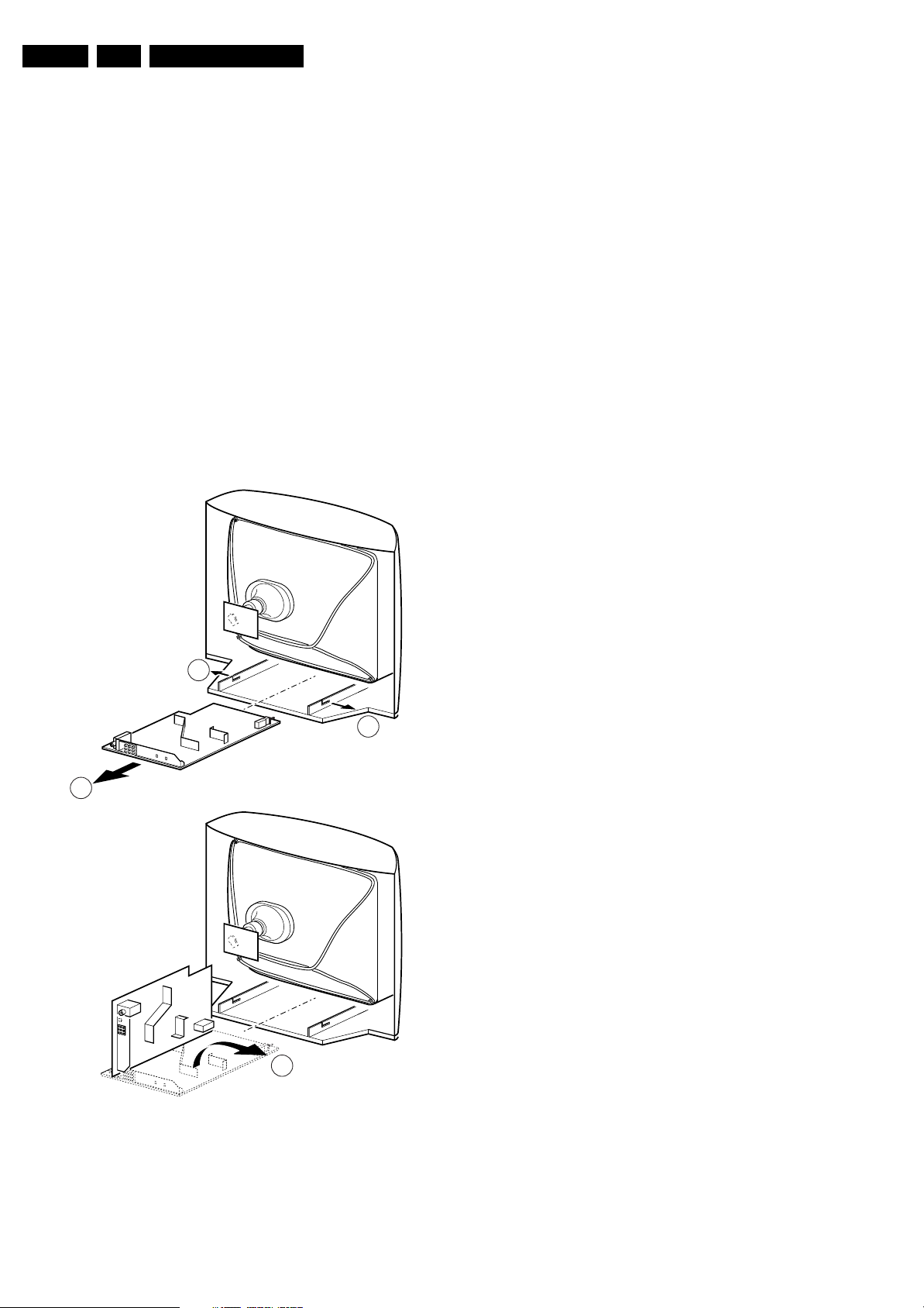
4.2 Service Position Main Panel
1. Disconnect the strain relief of the AC power cord.
2. Remove the main panel, by pushing the two center clips
outward [1]. At the same time pull the panel away from the
CRT [2].
3. If necessary, disconnect the degaussing coil by removing
the cable from the (red) connector 1512.
4. Move the panel somewhat to the left and flip it 90 degrees
[3], with the components towards the CRT.
4.3 Rear Cover Mounting
Before you mount the rear cover, perform the following checks:
1. Check whether the mains cord is mounted correctly in its
guiding brackets.
2. Re-place the strain relief of the AC power cord into the
cabinet.
3. Check whether all cables are replaced in their original
position
1
1
2
A
3
B
CL 16532016_006.eps
220501
Figure 4-1 Service Position
Page 7
Service Modes, Error Codes, and Fault Finding
5. Service Modes, Error Codes, and Fault Finding
EN 7L03.2L AA 5.
Index of this chapter:
5.1 Test Points
5.2 Service Modes
5.3 Problems and Solving Tips
5.4 ComPair
5.5 Error Codes
5.6 The Blinking LED Procedure
5.7 Protections
5.8 Repair Tips
5.1 Test Points
This chassis is equipped with test points in the service printing.
In the schematics test points are identified with a rectangle box
around Fxxx or Ixxx. On the PCB, test points are specifically
mentioned in the service manual as “half moons” with a dot in
the center.
Perform measurements under the following conditions:
• Service Default Alignment Mode.
• Video: color bar signal.
• Audio: 3 kHz left, 1 kHz right.
5.2 Service Modes
Service Default Alignment Mode (SDAM) offers several
features for the service technician.
There is also the option of using ComPair, a hardware interface
between a computer (see requirements below) and the TV
chassis. It offers the ability of structured trouble shooting, test
pattern generation, error code reading, software version
readout, and software upgrading.
Minimum Requirements: a Pentium Processor, Windows 95/
98, and a CD-ROM drive (see also paragraph “ComPair”).
• All picture settings at 50 % (brightness, color contrast,
hue).
• Bass, treble and balance at 50 %; volume at 25 %.
• All service-unfriendly modes (if present) are disabled, like:
– (Sleep) timer,
– Child/parental lock,
– Blue mute,
– Hotel/hospitality mode
– Auto switch-off (when no “IDENT” video signal is
received for 15 minutes),
– Skip / blank of non-favorite presets / channels,
– Auto store of personal presets,
– Auto user menu time-out.
• Operation hours counter.
• Software version.
• Option settings.
• Error buffer reading and erasing.
• Software alignments.
How to enter SDAM
Use one of the following methods:
• Use a standard customer RC-transmitter and key in the
code 062596 directly followed by the “M” (menu) button or
• Short jumper wires 9257 and pin 4 of 7200 on the mono
carrier (see Fig. 8-1) and apply AC power. Then press the
power button (remove the short after start-up).
Caution: Entering SDAM by shortening wires 9257 and pin
4 of 7200 will override the +8V-protection. Do this only for
a short period. When doing this, the service-technician
must know exactly what he is doing, as it could lead to
damaging the set.
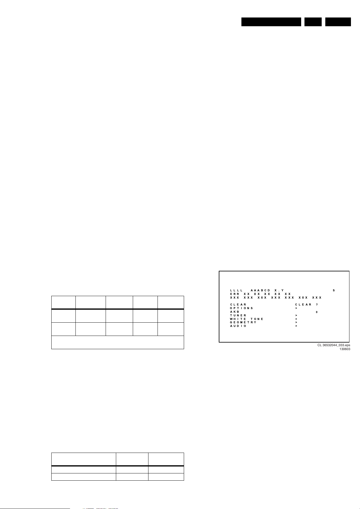
• Or via ComPair.
After entering SDAM, the following screen is visible, with S at
the upper right side for recognition.
Table 5-1 SW Cluster
SW
Cluster
Software
name UOC type
UOC
Diversity
L3SUM1 L03UM1 x.y TDA9377 55K
ROM Size
L3SUN1 L03UN1 x.y TDA9377 55K
ROM Size
Abbreviations in Software name:
U = Nafta, M = Mono, N = Stereo.
5.2.1 Service Default Alignment Mode (SDAM)
Purpose
• To change option settings.
• To create a predefined setting to get the same
measurement results as given in this manual.
• To display / clear the error code buffer.
• To override SW protections.
• To perform alignments.
• To start the blinking LED procedure.
Specifications
Table 5-2 SDM default settings
Region Freq. (MHz)
Europe, AP-PAL/Multi 475.25 PAL B/G
NAFTA, AP-NTSC, LATAM 61.25 (ch. 3) NTSC M
Special
Features
Mono
Stereo
(non DBX)
Default
system
CL 36532044_033.eps
130603
Figure 5-1 SDAM menu
• LLLL. This is the operation hours counter. It counts the
normal operation hours, not the standby hours.
• AAABCD-X.Y. This is the software identification of the
main micro controller:
– A = the project name (L03).
– B = the region: E= Europe, A= Asia Pacific, U= NAFTA,
L= LATAM.
– C = the feature of software diversity: N = stereo non-
DBX, S = stereo dBx, M = mono, D = DVD
– D = the language cluster number:
– X = the main software version number.
– Y = the sub software version number.
• S. Indication of the actual mode. S= SDAM= Service
Default Alignment mode.
• Error buffers. Five errors possible.
• Option bytes. Seven codes possible.
Page 8

EN 8 L03.2L AA5.
Service Modes, Error Codes, and Fault Finding
• Clear. Erase the contents of the error buffer. Select the
CLEAR menu item and press the CURSOR RIGHT key.
The content of the error buffer is cleared.
• Options. To set the Option Bytes. See chapter 8.3.1 for a
detailed description.
• AKB. Disable (0) or enable (1) the “black current loop”
(AKB = Auto Kine Bias).
• Tuner. To align the Tuner. See chapter 8.3.2 for a detailed
description.
• White Tone. To align the White Tone. See chapter 8.3.3
for a detailed description.
• Geometry. To align the set geometry. See chapter 8.3.4
for a detailed description.
• Audio. Use default value (Stereo set only), align when
necessary. See chapter 8.3.x for a detailed description.
How to navigate
• In SDAM, select menu items with the CURSOR UP/DOWN
key on the remote control transmitter. The selected item
will be highlighted. When not all menu items fit on the
screen, move the CURSOR UP/DOWN key to display the
next / previous menu items.
• With the CURSOR LEFT/RIGHT keys, it is possible to:
– Activate the selected menu item.
– Change the value of the selected menu item.
– Activate the selected submenu.
• When you press the MENU button twice, the set will switch
to the normal user menus (with the SDAM mode still active
in the background). To return to the SDAM menu press the
OSD / STATUS button.
• When you press the MENU key in a submenu, you will
return to the previous menu.
White line around picture elements and text
Decrease the SHARPNESS value when:
• The picture improves after you have pressed the “Smart
Picture” button on the remote control.
The new “Personal” preference value is automatically stored.
Snowy picture
• No or bad antenna signal. Connect a proper antenna
signal.
• Antenna not connected. Connect the antenna.
• No channel / pre-set is stored at this program number. Go
to the INSTALL menu and store a proper channel at this
program number.
• The tuner is faulty (in this case the CODES line will contain
error number 10). Check the tuner and replace / repair if
necessary.
Snowy picture and/or unstable picture
• A scrambled or decoded signal is received.
Black and white picture
Increase the COLOR value when:
• The picture improves after you have pressed the “Smart
Picture” button on the remote control.
The new “Personal” preference value is automatically stored.
Menu text not sharp enough
Decrease the CONTRAST value when:
The picture improves after you have pressed the “Smart
Picture” button on the remote control.
The new “Personal” preference value is automatically stored.
How to store settings
To store settings, leave the SDAM mode with the Standby
button on the remote.
How to exit
Switch the set to STANDBY by pressing the power button on
the remote control (if you switch the set 'off' by removing the AC
power, the set will return in SDAM when AC power is reapplied). The error buffer is not cleared.
5.3 Problems and Solving Tips
5.3.1 Picture Problems
Note: Below described problems are all related to the TV
settings. The procedures to change the value (or status) of the
different settings are described.
No colors / noise in picture
1. Press the MENU button on the remote control.
2. Select the INSTALLATION sub menu.
3. Select and change the SYSTEM setting until picture and
sound are correct.
4. Select the STORE menu item.
Colors not correct / unstable picture
1. Press the MENU button on the remote control.
2. Select the INSTALLATION sub menu.
3. Select and change the SYSTEM setting until picture and
sound are correct.
4. Select the STORE menu item.
5.3.2 Sound Problems
No sound or sound too loud (after channel change / switching on)
Increase / decrease the VOLUME level.
Press the Smart Sound button repeatedly to access 4 different
types of sound settings and choose your desired setting.
5.4 ComPair
5.4.1 Introduction
ComPair (Computer Aided Repair) is a service tool for Philips
Consumer Electronics products. ComPair is a further
development on the European DST (service remote control),
which allows faster and more accurate diagnostics. ComPair
has three big advantages:
• ComPair helps you to quickly get an understanding on how
to repair the chassis in a short time by guiding you
systematically through the repair procedures.
• ComPair allows very detailed diagnostics (on I
is therefore capable of accurately indicating problem areas.
You do not have to know anything about I
yourself because ComPair takes care of this.
• ComPair speeds up the repair time since it can
automatically communicate with the chassis (when the
microprocessor is working) and all repair information is
directly available. When ComPair is installed together with
the SearchMan electronic manual of the defective chassis,
schematics and PWBs are only a mouse click away.
5.4.2 Specifications
2
C level) and
2
C commands
Picture too dark or too bright
Increase / decrease the BRIGHTNESS and / or the
CONTRAST value when:
• The picture improves after you have pressed the “Smart
Picture” button on the remote control.
• The picture improves after you have switched on the
Customer Service Mode
The new “Personal” preference value is automatically stored.
ComPair consists of a Windows based faultfinding program
and an interface box between PC and the (defective) product.
The ComPair interface box is connected to the PC via a serial
or RS232 cable.
In this chassis, the ComPair interface box and the TV
communicate via a bi-directional service cable via the service
Page 9

Service Modes, Error Codes, and Fault Finding
EN 9L03.2L AA 5.
connector (located on the Main panel, (see figure "Top view
Mono Carrier" in chapter 8 "Alignments").
The ComPair faultfinding program is able to determine the
problem of the defective television. ComPair can gather
diagnostic information in two ways:
• Automatic (by communication with the television):
ComPair can automatically read out the contents of the
entire error buffer. Diagnosis is done on I
can access the I
and receive I
2
C bus of the television. ComPair can send
2
C commands to the micro controller of the
television. In this way, it is possible for ComPair to
communicate (read and write) to devices on the I
2
C level. ComPair
2
C busses
of the TV-set.
• Manually (by asking questions to you): Automatic
diagnosis is only possible if the micro controller of the
television is working correctly and only to a certain extent.
When this is not the case, ComPair will guide you through
the faultfinding tree by asking you questions (e.g. Does the
screen give a picture? Click on the correct answer: YES /
NO) and showing you examples (e.g. Measure test-point I7
and click on the correct oscillogram you see on the
oscilloscope). You can answer by clicking on a link (e.g.
text or a waveform picture) that will bring you to the next
step in the faultfinding process.
By a combination of automatic diagnostics and an interactive
question / answer procedure, ComPair will enable you to find
most problems in a fast and effective way.
Besides fault finding, ComPair provides some additional
features like:
• Up- or downloading of pre-sets.
• Managing of pre-set lists.
• Emulation of the Dealer Service Tool (DST).
• If both ComPair and SearchMan (Electronic Service
Manual) are installed, all the schematics and the PWBs of
the set are available by clicking on the appropriate
hyperlink.
Example: Measure the DC-voltage on capacitor C2568
(Schematic/Panel) at the Mono-carrier.
– Click on the 'Panel' hyperlink to automatically show the
PWB with a highlighted capacitor C2568.
– Click on the 'Schematic' hyperlink to automatically
show the position of the highlighted capacitor.
PC VCR I2CPower
Figure 5-2 ComPair connection
5.4.4 How to Order
ComPair order codes (EU/AP/LATAM):
• Starter kit ComPair32/SearchMan32 software and
ComPair interface (excl. transformer): 3122 785 90450.
• ComPair interface (excl. transformer): 4822 727 21631.
• Starter kit ComPair32 software (registration version): 3122
785 60040.
• Starter kit SearchMan32 software: 3122 785 60050.
• ComPair32 CD (update): 3122 785 60070 (year 2002),
3122 785 60110 (year 2003 onwards).
• SearchMan32 CD (update): 3122 785 60080 (year 2002),
3122 785 60120 (year 2003), 3122 785 60130 (year 2004).
• ComPair firmware upgrade IC: 3122 785 90510.
• Transformer (non-UK): 4822 727 21632.
• Transformer UK: 4822 727 21633.
• ComPair interface cable: 3122 785 90004.
• ComPair interface extension cable: 3139 131 03791.
5.4.5 Error Buffer
The error code buffer contains all detected errors since the last
time the buffer was erased. The buffer is written from left to
right. When an error occurs that is not yet in the error code
buffer, it is written at the left side and all other errors shift one
position to the right.
5.4.6 How To Read the Error Buffer
I2C SERVICE
CONNECTOR
9V DC
E_06532_008.eps
180804
TO
5.4.3 How to Connect ComPair
1. First, install the ComPair Browser software (see the Quick
Reference Card for installation instructions).
2. Connect the RS232 interface cable between a free serial
(COM) port of your PC and the PC connector (marked with
“PC”) of the ComPair interface.
3. Connect the AC power adapter to the supply connector
(marked with “POWER 9V DC”) on the ComPair interface.
4. Switch the ComPair interface OFF.
5. Switch the television set OFF (remove the AC power).
6. Connect the ComPair interface cable between the
connector on the rear side of the ComPair interface
(marked with “I
2
C”) and the ComPair connector on the
mono carrier (see figure "Top view Mono Carrier" in
chapter 8 "Alignments").
7. Plug the AC power adapter in the AC power outlet and
switch on the interface. The green and red LEDs light up
together. The red LED extinguishes after approx. 1 second
while the green LED remains lit.
8. Start the ComPair program and read the “introduction”
chapter.
You can read the error buffer in 3 ways:
• On screen via the SDAM (only if you have a picture).
Examples:
– ERROR: 0 0 0 0 0: No errors detected
– ERROR: 6 0 0 0 0: Error code 6 is the last and only
detected error
– ERROR: 9 6 0 0 0: Error code 6 was first detected and
error code 9 is the last detected (newest) error
• Via the blinking LED procedure (when you have no
picture). See next paragraph.
•Via ComPair.
5.4.7 How to Clear the Error Buffer
The error code buffer is cleared in the following cases:
• By activation of the CLEAR command in the SDAM menu:
• If the content of the error buffer has not changed for 50
hours, it resets automatically.
Note:
When leaving SDAM by disconnecting the set from AC power,
the error buffer is not reset.
Page 10
EN 10 L03.2L AA5.
5.5 Error Codes
In case of non-intermittent faults, clear the error buffer before
you begin the repair. These to ensure that old error codes are
no longer present.
If possible, check the entire contents of the error buffer. In
some situations, an error code is only the result of another error
code and not the actual cause (e.g., a fault in the protection
detection circuitry can also lead to a protection).
Table 5-3 Error Code Table
ERROR Device Error description Check item Diagram
0 Not applicable No Error - 1 Not applicable X-Ray Protection (USA) 7421, 2423, 6421, 6422 A2
2 Not applicable Horizontal Protection 7421, 7422, 7423 A2
3 Not applicable Vertical Protection 7461, 7462, 7463, 7464, 7465, 7466 A2
4 TDA9853H Tone control & Audio processor I
identification error
5 TDA93XX POR 3.3V / 8V Protection 7200, 7541, 7491, 7493, 7496 A4, A1
6I
7 Not applicable - - 8 Not applicable E/W Protection (Large Screen) - 9M24C16 NVM I
10 Tuner Tuner I
11 Not applicable Black current loop protection 3313, 7307, 7308, 7309, 7310, 7311, 7312, 7313,
12 Not applicable MAP I
13 Not applicable VC I
14 Not applicable DVD I
2
C bus General I2C bus error 7200, 3604, 3605 A4
2
C identification error 7641, 3641, 3642, 3643 A4
2
C identification error 1000, 3003, 3004 A3
2
C identification error (USA) - -
2
C identification error (Eu) - -
2
C identification error - -
Service Modes, Error Codes, and Fault Finding
2
C
7861 (Stereo/Sap) A5
7314, 7315, 7316, 7317, 7318, CRT
B1
5.6 The Blinking LED Procedure
Via this procedure, you can make the contents of the error
buffer visible via the front LED. This is especially useful when
there is no picture.
When the SDAM is entered, the LED will blink the contents of
the error-buffer.
• n short blinks (n = 1 - 14),
• When all the error-codes are displayed, the sequence
finishes with a LED blink of 3 s,
• The sequence starts again.
Example of error buffer: 12 9 6 0 0
After entering SDAM:
• 12 short blinks followed by a pause of 3 s,
• 9 short blinks followed by a pause of 3 s,
• 6 short blinks followed by a pause of 3 s,
• 1 long blink of 3 s to finish the sequence,
• the sequence starts again.
5.7 Protections
If a fault situation is detected an error code will be generated
and if necessary the set will be put in the protection mode.
Blinking of the red LED at a frequency of 3 Hz indicates the
protection mode. In some error cases, the microprocessor
does not put the set in the protection mode. The error codes of
the error buffer can be read via the service menu (SDAM), the
blinking LED procedure or via ComPair.
To get a quick diagnosis the chassis has one service modes
implemented:
• The Service Default Alignment Mode (SDAM). Start-up of
the set in a predefined way and adjustment of the set via a
menu and with the help of test patterns.
5.8 Repair Tips
Below some failure symptoms are given, followed by a repair
tip.
• Set is dead and makes hiccupping sound. “Main
Supply” is available. Hiccupping stops when de-soldering
L5563, meaning that problem is in the “Main Supply” line.
No output voltages at LOT, no horizontal deflection.
Reason: line transistor 7421 is defective.
• Set is dead, and makes no sound. Check power supply
IC 7520. Result: voltage at pins 2, 6, 7, 9 and 11 are about
180 V and pin 14 is 0 V. The reason why the voltage on
these pins is so high is because the output driver (pin 11)
has an open load. That is why MOSFET 7521 is not able to
switch. Reason: feedback resistor 3523 is defective.
Caution: be careful measuring on the gate of 7521;
circuitry is very high ohmic and can easily be damaged!
• Set is in hiccup mode and shuts down after 8 s. Blinking
LED (set in SDM mode) indicates error 5. As it is unlikely
that the “POR” and “+8V protection” happen at the same
time, measure the “+8V”. If this voltage is missing, check
transistor 7491 and 7496.
• Set is non-stop in hiccup mode. Set is in over current
mode; check the secondary sensing (opto coupler 7515)
and the “Main Supply” voltage. Signal “Stdby_con” must be
logic low under normal operation conditions and goes to
high (3.3 V) under standby and fault conditions.
• Set turns on, but without picture and sound. The screen
shows snow, but OSD and other menus are okay. Blinking
LED procedure indicates error 11, so problem is expected
in the tuner (pos. 1000). Check presence of supply
voltages. As “Vlotaux+5V” at pin 5 and 7 are okay,
“VT_supply” at pin 9 is missing. Conclusion: resistor 3449
and 3450 are defective
Page 11
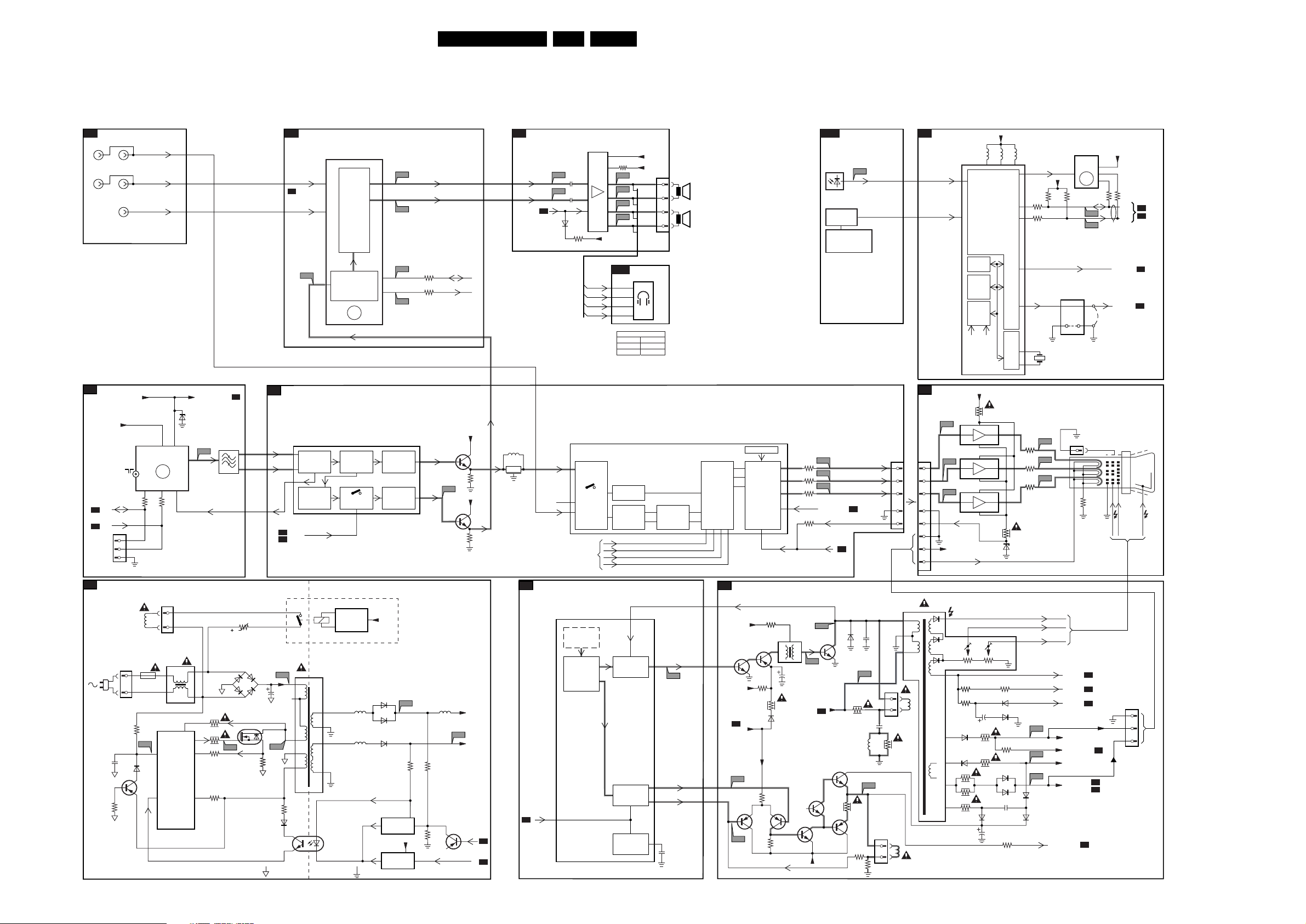
Block Diagrams, Testpoint Overviews, and Waveforms
6. Block Diagrams, Testpoint Overviews, and Waveforms
Block Diagram
EN 11L03.2L AA 6.
A7
V
L
A3
FRONT I/O
MONO
TUNER IF
A4
A4
ComPair
CONN.
SDA
SCL
STEREO
V
L
R
VT_SUPPLY
+5V
1003
1
2
3
SDA
SCL
1000
UV1336
2
SY_CVBS_IN
L1_IN
R1_IN
6, 7 9
TV TUNER
ERR
10
5
4
3004
3003
AGC
VT
1
6001
BZX79-C33
11
IF
VT_SUPPLY_A
1001
T1
TUNER_AGC
AUDIO PROCESSING (BTSC STEREO DECODER)
A5
7861
TDA9853H
L1_IN
8
26
4
(MONO)
INPUT
SELECT
BTSC STEREO
+
DECODER
ERR
4
VIDEO
PLL
DEMOD.
AUDI O
SWITCH
35
A8
R1_IN
A1
IF, VIDEO PROCESSING
VIF_1
VIF_2
A4
7200-A
TDA93XX
23
VIDEO
IF
24
AGC
27
SOUND
FM-DEMOD.
DE-EMPH.
A5
L1_IN
A7
A2
A5
1
18
A4
A3
38
18
A2
VIDEO
AMPLIFIER
SOUND
AMPL.
+ AVL
Main_OutL
Main_OutR
3865
3866
38
44
SDA
SCL
AM_FM_MONO
+8VD
V1
+8V
AUDIO CARRIER
7201
3205
7202
3203
FILTER
5201
1201
4.5MHz
A6
AUDIO AMPLIFIER
Main_OutL
Main_OutR
A4
N.C.
SY_CVBS_IN
7901 AN7522N (STEREO)
7902 AN7523N (MONO)
A6
2904
62
A7
2906
8
VOLUME
9
1
6909
3911
7200-C
TDA93XX
40
SWITCHING
VIDEO
43
FILTERS
42
VIDEO
IDENT
1
3901
5
A8
A9
4L-
A10
10 R-
A11
12 R+
FILAMENT
HEADPHONE
A7
L+
L-
R-
R+
I/O
N.C.
L+
L-
R-
R+
SPEAKER
2 X 5W 16 Ohm
2 X 3W 8 Ohm
2 X 1W 8 Ohm
Y-DELAY
PAL/NTSC
DECODER
R_SC1_IN_V_IN
G_SC1_IN_Y_IN
B_SC1_IN_U_IN
FBL_SC1_IN
Vaudio
+5V
L+
R-Y
B-Y
1900
4
5
1
2
BASE
BAND
DELAY
L
R
Y
U
V
RGB
MATRIX
RGB
INSERT
BLACK
STRETCH
WHITE
STRETCH
4746 48
45
R
CONTROL
G
OSD/TEXT/CC
B
STRETCH
OSD
RGB
INSERT
BLUE
WHITE-P.
ADJ
50
3619
51
3620
52
3621
53
49
3624
A7
6692
TSOP1836
KEYBOARD
POWER (USA only)
V9
V10
V11
BEAM-LIMIT
BLK_IN
FRAME_OUT
FRONT CONTROL
F1
1
LOCAL
CHANNEL + / -
VOLUME + / -
RED
GREEN
BLUE
A2
A2
CONTROL
A4
KEYBOARD
B1
1300
1
2
3
4
5
6
7
8
CRT
IR
62
8
7308
7313
7314
V12
7310
7315
7316
V13
7312
7317
7318
V14
+170V0
IR
1622
1
2
3
4
5
7200-B
TDA93XX
ROM
RAM
1/10
PAGES
MEMORY
TELE
TEXT/CC
OSD
CVBS
+170V0
R
G
B
FILAMENT
54 61 56
IIC
BUS
I/O
PORTS
VST
PWM-
DAC
+
SYNC
3313
+3.3V
56035601
5602
CPU
3318
6318
WP
11 7
+3V3
3605
3
3604
2
1
4
57
1621
58
12MHz
V15
3301
R
V16
3305
G
B
V17
3309
7641
M24C04
EEPROM
(NVM)
ERR
9
36013602
SDA
V7
SCL
V8
9625
0165
AQUADAG
7
R
9
G
3
B
45 68
3319
+3.3V
8
6
5
36423643
SDA
A3
A5
SCL
Std_Con
A1
VOLUME
SDAM
VG2 FOCUS EHT
A6
CRT
(9P)
25kV
POWER SUPPLY
A1
90VAC-130VAC
low range
Degaussing
1511
2521
7523
3528
SYNC.
A4
1512
3527
3523
3525
3522
6500
6502
P6
3503
t
P1
6501
2504
6503
7521
D
G
S
P5
3526
3581
HOT GROUND COLD GROUND
Coil
5502
1500
T4E
7520
14
TEA1506
3506
DRAIN
11
2
Vcc
6
CTRL
CONTROL
IC
DRIVER
SENSE
DEMAG
9
7
P4
6520
1
2
3
5
6
6522
4
3
5520
1515
43
2
1
11
10
8
7
1
7515
TCET1103
2
7580
ENERGIZING
CIRCUIT
(optional)
5562
5560
RESERVED
-12V
6562
6561
6560
7540, 6540
REFERENCE
7541
CIRCUIT
+3V3A
STANDBY
CIRCUIT
7200-D
TDA93XX
VIDEO
INTERNAL
H/V SYNC
SEPERATOR
H-OSC
+PLL
P2
3549
3543
3544
7451
5563
MAIN SUPPLY
Vaudio
P3
Std_Con
EHT
EHT0
36
A2
A2
A4
H
V
34
H-DRIVE
2nd LOOP
H-SHIFT
V-D RVE
+
GEOMETRY
EW
+
GEOMETRY
H-DRIVE
33
V2
V-DRIVE -
22
V-DRIVE +
21
20
2490
A2
Vaudio
FILAMENT
DEFLECTION
Hflybk
-12V
7422
A2
D4
7461
D5
7423
3425
3424
3463
3423
6423
7462
3465
5421
LINE
2428
FRAME
BUT11APX
D2
MAINSUPPLY
7466
7463
-12V
5441
2423
0221
1
4
2406
5401 3402
1402
1
2
1
7
2
HOR.
DEFL.
COIL
VERT.
DEFL.
COIL
D3
7421
A1
6422
D1
3403
7464
D7
3470
7465
3464
3474
EHT
10
9
8
5
4
FOCUS VG2
3447
3451
2455
3448
6447
3445
6446
3443
3444
3446
6463
2465
3410
6451
6452
3459
6448
6444
2460
3475
6461
6462
D8
D9
D10
EHT
FOCUS
VG2
EHT
EHT 0
BEAMLIMIT
+160VD
VT SUPPLY
-12V
FILAMENT
FRAME OUT
A1
A4
A4
+160VD
A6
A2
A4
1400
A3
FILAMENT
E_14560_017.eps
1
2
3
240304
Page 12
Block Diagrams, Testpoint Overviews, and Waveforms
pp
pp
)
pp
pp
(
,
,
pp
pp
)
,
,
pp
pp
pp
)
I2C and Supply Voltage Overview
EN 12L03.2L AA 6.
POWER SUPPLY
A1
90VAC-130VAC
low range
2521
3528
Degaussing
1511
7523
Coil
3506
6520
1500
T4E
7520
TEA1506
2
Vcc
6
CTRL
1512
5502
DRAIN
DRIVER
SENSE
DEMAG
CONTROL
IC
DEFLECTION
A2
CIRCUIT
(optional)
5562
5560
RESERVED
-12V -12V
6562
6561
6560
7540, 6540
REFERENCE
CIRCUIT
+3V3A
7541
STANDBY
CIRCUIT
3549
5563
3543
3544
7451
EHT
Std_Con
Vaudio
A2
+3V3A
A4
1x
2x
-12V
H-DRIVE
Vaudio
MAINSUPPLYMAINSUPPLY
FILAMENT
V-DRIVE-
V-DRIVE+
7422
7461
7423
3425
3424
3463
3423
6423
7462
3465
5421
2428
FRAME
BUT11APX
7463
7466
-12V
7421
7464
7465
3403
3470
3464
3474
6422
5401
2423
1402
1
2
0221
1
4
2406
3402
1
7
2
HOR.
DEFL.
COIL
5441
VERT.
DEFL.
COIL
EHT
FOCUS VG2
10
3447
3451
6447
9
6446
8
3443
5
3444
3446
4
2455
3448
3445
6463
2465
3410
6451
6452
3459
6448
6444
2460
3475
EHT
EHT 0
BEAMLIMIT
6461
6462
EHT
FOCUS
VG2
A1
A4
A4
FRAME OUT
+160VD
VT SUPPLY
-12V
FILAMENT
A4
+160VD
FILAMENT
A3
A6
1400
2
3
VT SUPPLY
7580
1515
43
3503
t
6501
6500
6503
6502
3527
14
3523
11
3525
9
3522
7
7521
G
D
S
3526
HOT GROUND COLD GROUND
2504
1
2
3
5
6
3581
6522
2
5520
4
3
1
11
10
8
7
1
7515
TCET1103
2
ENERGIZING
B1
1300
7
8
-12V
FILAMENT
CRT
EHT
FOCUS
VG2
170 V0
3313
1x
3x
2x
To VIDEO
OUTPUTS
FILAMENT
I2C BUS INTERCONNECTION DIAGRAM
VIDEO PROCESSING
A4
SDA
7200-B
SET
PROCESSOR
PAR T O F
VIDEO-
PROCESSOR
TDA93XX
ERROR CODE LIST
Error Device Error description Check item Diagram
0 Not a
1 Not a
2 Not a
3 Not a
4 TDA9853H
5 TDA93XX POR 3.3V / 8V Protection 7200
6 I2C bus General I2C bus error 7200
7 Not a
8 Not a
9 M24C16 NVM I2C identification error 7641
10 Tuner Tuner I2C identification error 1000
11 Not a
12 Not a
13 Not a
14 Not applicable DVD I2C identification error - -
licable No Error - licable X-Ray Protection (USA
licable Horizontal Protection 7421, 7422, 7423 A2
licable Vertical Protection
licable - - licable E/W Protection (Large Screen
licable Black current loop protection
licable MAP I2C identification error (USA)-licable VC I2C identification error (Eu
3
2
SCL
11
Tone control & Audio processor I2C
identification error 7861
+3.3V
+3.3V
ERR
3602
3605
3604
WP
7421, 2423, 6421, 6422 A2
7461, 7462, 7463, 7464, 7465,
7466 A2
--
3313, 7307, 7308, 7309, 7310,
7311, 7312, 7313, 7314, 7315,
7316, 7317, 7318, CRT B1
--
3601
+3.3V
Stereo/Sap) A5
7541, 7491, 7493, 7496 A4, A1
3604, 3605 A4
3641, 3642, 3643 A4
3003, 3004 A3
3644
EEPROM
7
3643
7641
M24C16
(NVM)
ERR
6
3642
65
9
SDA
SCL
A3
TUNER IF
3003
1000
TUNER
UV1336
ERR
VIDEO PROCESSING
A4
B1
Vaudio
AUDIO BTSC STEREO
A5
DECODER
(economic)
SDA
SCL
3004
45
10
1003
1
2
FOR
COMPAIR
ONLY
3
3865
3866
4038
7861
TDA9853H
AUDIO
PROC.
ERR
4
Vau dio
FILAMENT
VTSupply-A
3496
6492
1
7494
7493
3
6491
In
3497
4379
3493
7491
3491
3492
7496
3494
+3V3
4491
A1
A2
3495
5482
+8V
+3V3A
+5V
+8V
+8VD
1x
2x
1x
1x
1x
TUNER IF
A3
+ 5 V
VT supply
VT Supply-A
AUDIO PROCESSING
A5
+ 8V
AUDIO AMPLIFIER
A6
Vau dio
+ 5V
FILAMENT
AUDIO FRONT I/O
A7
+ 3V3A
6001
-/C33
5861
+ 5 V
VT supply
41 - 7861
1 - 7901
or
1 - 7902
+ 5V
FILAMENT
+3V3A
F_15380_001.eps
050405
Page 13
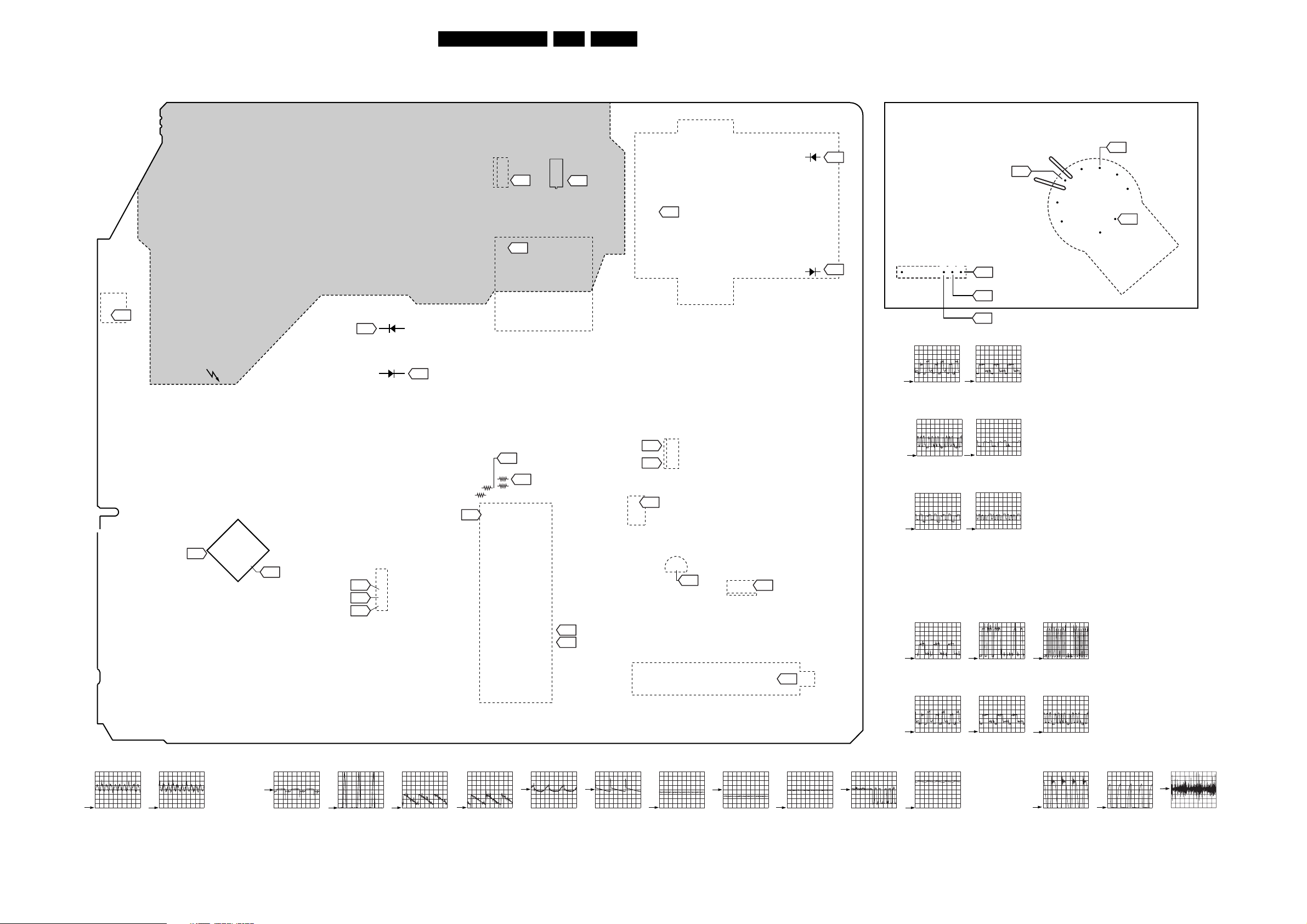
Block Diagrams, Testpoint Overviews, and Waveforms
Testpoint Overview Mono Carrier and CRT Panel
EN 13L03.2L AA 6.
CRT TRACK SIDE VIEWMONO CARRIER TRACK SIDE VIEW
6692
3
1
7521
7520
S
D
G
P6
16
P1
2
P4
5520
6461
D9
V15
3
2
D1
1
LOT
5441
8
9
10
6447
D8
1300
8
231
V14
7
6
5
V16
8
9
10
11
3
V17
4
1302
CRT
Socket
V13
F1
HOT
COLD
AUDIO
PROC.
34
7861
1
A5
23
18
A4
12
V11
V10
V9
6560
P3
6561
11
7
V12
P2
1V / div DC
20µs / div.
V14
7421
B
1622
5
4
3
2
1
3601
V2
3642
V8
3643
3602
7200
VIDEO
PROC.
D2
D3
V7
1000
3
D10
133
21
D5
22
D4
2
1
C
E
7463
EBC
D6
7464
B
1V / div DC
20µs / div.
V16
50V / div DC
20µs / div.
E
D7
C
V2
V12
V13
1V / div DC
20µs / div.
V15
50V / div DC
20µs / div.
V17
50V / div DC
20µs / div.
V7
V8
A4
0.5V / div DC
1ms / div.
A5
0.5V / div DC
1ms / div.
D1 97V DC
D2
5V / div AC
20µs / div.
D3
100V / div DC
20µs/div.
D4
0.5V / div DC
5ms / div.
D5
0.5V / div DC
5ms / div.
3264
D6
1V / div AC
5ms / div.
D7
20V / div DC
5ms / div.
11
D8
50V / div DC
20µs / div.
1000
TUNER
D9
10V / div DC
20µs / div.
1
T1
D10
2V / div DC
20µs / div.
F1
1V / div AC
2ms / div.
0,5V / div DC
20µs / div.
V9
1V / div DC
20µs / div.
P1
50V / div DC
5µs / div.
0.5V / div DC
20µs / div.
V10
1V / div DC
20µs / div.
P2 97V DC
P3 13V5 DC
P4 17V8 DC
0,5V / div DC
20µs / div.
V11
1V / div DC
20µs / div.
P5
100V / div DC
5µs / div.
P6
2V / div DC
5µs / div.
T1
200mV / div AC
20µs / div.
E_14560_019.eps
180304
Page 14

Circuit Diagrams and PWB Layouts
7. Circuit Diagrams and PWB Layouts
Mono Carrier: Power Supply
1234567891011
POWER SUPPLY
A
DEGAUSSING COIL
1512
1
16V2
12V6
22u
1n0
1V2
3520
2505
*
3
6
1K2
2n2
PFC5000
6505
BZX384-C22
9505
7520
TEA1506
Vcc
Gnd
Ctrl
10n
2520
1500
T4E.250V
33K3507
FREQUENCY
INPUT
CONTROL
CIRCUIT
BURST
DETECTOR
CONTROL
1501
PFC5000
2500
SUPPLY
MANAGEMENT
TEMPERATURE
220n
3505
3509
VOLTAGE
CONTRLLED
OSCILLATOR
OVER
PROTECTIOM
POWER-ON
RESET
220R
V
3510
DSP
6
C914 31
330K
LOGIC
CONTROL
CIRCUIT
MAXIMUM
ON-TIME
PROTECTION
B
C
D
E
F
G
3139 123 5802.1
2
1511
2
1
MAINS
90VAC-130VAC
LOW RANGE
3M3
3500
L_GND
3501
3M3
1520
P4
2521
6520
2526
BYV95A
RES
7523
BC857B
5V2
2527
0V0
56p
10K
3528
"$"
FOR MAINS 120V AC 170V (177V)
..V.. Normal Operation in " SERVICE MODE "
(..V..) Standy Mode
*
3V8
RES
3521
220V AC 309V (317V)
HOT GROUND
COLD GROUND
12345
5502
3506
4
VALLEY
3503
*
3508
*
1M5
START-UP
CURRENT SOURCE
START-UP
CURRENT SOURCE
CURRENT
SENSING
OUTPUT
DRIVER
OVER
POWER
PROTECTION
+t
10R - PTC
9502
3502
t
RES
Drain
Demag
Sense
Driver
EN 14L03.2L AA 7.
1500 B2
1501 B3
1511 C1
1512 B1
1515 A7
1520 D1
1521 D9
2452 F11
2453 F10
2500 C3
2501 B5
2502 B5
2504 B6
2505 B2
2507 B6
2515 C7
2520 G2
2521 E2
2522 D6
2523 E6
2524 E5
2525 F5
2526 E2
2527 F1
2528 G6
2540 F9
2541 G9
2542 G7
2543 F6
2560 D8
2561 D9
2562 D9
2564 D10
2580 B7
2584 C6
3452 F11
3453 F10
3454 F9
3456 F11
3500 C2
3501 D2
3502 C4
3503 B4
3505 C3
3506 D4
3507 D2
3508 B4
3509 D3
3510 D3
3519 F6
3520 G2
3521 F2
3522 E5
3523 E5
3524 E5
3525 E5
3526 E6
3527 D5
3528 F1
3541 F8
3542 E9
3543 E10
3544 F9
3545 G8
3547 F10
3548 F9
3549 E9
3580 A7
3581 F6
3582 D10
4501 E5
5502 C4
5509 E8
5520 C7
5521 D6
5560 D8
5562 C9
5563 D10
6500 B5
6501 B6
6502 B5
6503 B6
6505 D2
6520 E2
6522 F6
6540 F8
6541 E9
6560 D8
6561 D9
6562 C9
6580 A8
7451 F10
7515 F7
7520 D2
7521 E6
2501
2502
1N5062 (COL)
2n2
1N5062 (COL)
2n2
6500
6502
6501
1N5062 (COL)
6503
1N5062 (COL)
2504
400V
150u
For Relay Cct.
RES
1515
*
G5P
9503
*
14
23
-12V4
P1
"$"
RES
2507
*
2515
7580
BC847B
0V0
-12V
47K
3580
*
6580
*
2580
*
1N4148
-12V0
47u
Item
2523
2562
5520
6520
6522
P2 97V DC
P3 13V5 DC
P4 17V8 DC
13V/19V
1N8 1N5
2N2
SS28011-04
BYV95A
BYV95A
1n5
14RF
1N5
SS28032-02A
RGP15D
RGP15D
P1
50V / div DC
5µs / div.
P5
100V / div DC
5µs / div.
P6
2V / div DC
5µs / div.
A
B
C
5520
*
2584
1
130V0
220p
3
5
5521
470p
2522
P5
4501
3524
RES
2524
RES
3527
2K2
3522
330K
3525
1K0
3523
STP5NK50ZFP
7521
4V7
G
P6
142
114V3
8
10
7
0V0
9
0V0
11
4V7
0V0
D
S
3526
112V6
2523
0R15
6
1n8
*
112
10
8
7
AudioSupplyGnd_A
5560
9509
5509
AudioSupplyGndAudioSupplyGnd_A
6560
SB340
2560
2n2
AudioSupplyGnd_A
*
2525
470p
6540
3V3
3581
56R
3519
3K3
6522
*
BYV95A
2543
1n0
TCET1103(G)
16V5
2528
22u 50V
7515
4V6
HOT
1
4
32
9V1
8V0
COLD
2542
470n
3541
470R
3545
2K2
8V1
7541
PDTC114ET
3V3
P3
2561
3549
3542
BZX79-B6V8
7V4
2541
2m2 16V
220R
1K5
6V3
7540
BC547B
2540
15n
10n
5562
6541
6V9
2562
*
2n2
BZX79-C9V1
3548
15K
6562
BYW76
6561
*
1521
3544
6K8
3454
10K
3547
2564
P2
47u
3582
330K
5563
27u
MainSupply
Vaudio
D
E
82K
3543
2453
4n7
2452
82n
3452
820K
3456
47K
EHT
+3V3A
Std_Con
E_14560_003.eps
F
A2
A4
150304
G
7451
*
BC857B
8V8
9V1
3453
100K
7523 F1
7540 F9
7541 G8
7580 A7
9502 C4
9503 A6
9505 D2
9509 D8
6 7 8 9 10 11
Page 15

Mono Carrier: Deflection
1234567891011
DEFLECTION
A
B
C
D
E
F
G
H
3139 123 5802.1
Line Deflection
Hflybk
A4
-12V
RES
2471
HDRIVE
A4
6423
FILAMENT
A2
BAS316
Vaudio
MainSupply
Frame Deflection
FILAMENT
A2
VDrive-
A4
-12V
VDrive+
A4
3424
22R
2427
100n
3425
330R
D4
3461
D5
Circuit Diagrams and PWB Layouts
3422
330K
D2
2429
3423
1R
2K2
2426
2428
2461
3462
220n
1n
0V8
47u
1n
7461
BC857B
1M
6426
0V0
3430
1K0
2420
100n
BAS316
D1
5V6
-12V6
0V0
3V4
3432
3463
3465
7422
BC817-25
7423
1K
BC807-25
2K2
1V4
1K
3464
2K2
2421
100n
6V0
BC857B
-7V0
7462
-11V9
3428
3466
1K
68R
2462
0V9
3
1
PSD10-204B
1n
0V3
5421
6460
D6
-12V0
7421
BUT11APX
3426
47R
6
5
2405
2463
BAS316
2464
470p
47u
100u 50V
46V4
0V0
3403
1K
3468
330R
7463
BC546B
-12V5
6422
BYD33M
HORIZONTAL
DEFLECTION
COIL
6464
BAS316
7466
BC847B
0V0
0V0
0V0
2423
1401
0V0
VH
*
RES
9402
7464
BD135
10n
-12V5
2424
D3
1
4
2406
5402
0V0
*
*
3470
820p
470n
DC12
23V8
-0V5
7465
BD136
5401
2R2
2408
EN 15L03.2L AA 7.
1400 E10
1401 C4
1402 G6
1463 E8
1464 E11
2405 D3
Item
3473
3474
2406
2408
2423
2424
2441
3451
2455
8K2
*
10u 16V
*
2452
2494
3402
3440
3441
3442
3443
3444
3445
3447
3451
3455
3460
5441
*
6451
BAS316
3460
100K
D3
100V / div DC
20µs/div.
D8
50V / div DC
20µs / div.
LOT
5441
*
1142
EHT
TO PICTURE TUBE
FOCUS
TO CRT PANEL
VG2
8
6462
Frame_FB
3R3
6463
RGP10D
-12V
6
9
10
7
4
5
2460
56n
6461
RGP10D
3475
10K
3476
8K2
D7
3446
3447
*
100K
7440
BF423
*
33K
3439
470u
2446
D2
5V / div AC
20µs / div.
D7
20V / div DC
5ms / div.
3V5
140V0
3R3
BAS316
470u
3450
33K
RES
6452
3449
33K
6453
150K
1463
10u
137V0
3457
3440
2M2
BZX79-C33
2444
120K
3441
6445
2473
470p
BAS316
3443
*
1R
3444
*
1R
1R
1402
1
2
VH
VERTICAL
DEFLECTION
COIL
6446
RGP10D
6447
RGP10D
2457
470p
6448
6444
EGP20DL
3445
*
1R
120K
3459
3442
**
3448
1R
2447
D1 97V DC
D6
1V / div AC
5ms / div.
1
3
2
12n
*
2K2
3402
*
33u
RGP10D
160V
2465
10u
220R
220R
3R3
2470
3478
15n
1R0
3474
*
3471
3472
3473
*
3410
68K
2441
33n
19V 13V
3R3
3R3
NO
560N
15N15N
1N
33N
100N
NO
2K2
33K
47K
150K
3R9
3R9
1R
150K
8K2
2K2
47K
JF0501-19276
3455
*
2K2
MainSupplyGND
D10
D9
D8
D4
0.5V / div DC
5ms / div.
D9
10V / div DC
20µs / div.
4R7
4R7
NO
560N
13N
470P
22N
22N
NO
NO
36K
47K
100K
4R7
3R9
3R9
220K
680R
470R
100K
JF0501-19255
1400
1
2
3
14RF
3R3
3R3
360N
NO
12N
680P
15N
22N
47U
2K2
33K
10K
150K
3R9
4R7
100K
680R
470R
100K
JF0501-19255
DIPMATE
1464
TO 1300
OF CRT PANEL
D5
0.5V / div DC
5ms / div.
D10
2V / div DC
20µs / div.
1R
VTSupply
EHTO
EHT
Beam_Limit
FILAMENT
-12V
160VD
Frame_OUT
A4
A1
A4
A4
A4
E_14560_004.eps
A
B
C
D
E
F
G
H
150304
2406 D4
2408 D5
2420 B2
2421 B3
2423 A4
2424 A4
2426 B2
2427 B1
2428 D2
2429 B2
2441 C9
2444 E8
2446 E8
2447 E8
2455 D9
2457 E7
2460 E6
2461 F2
2462 F3
2463 F3
2464 F3
2465 F5
2470 F5
2471 B1
2473 C7
3402 D5
3403 D4
3410 C9
3422 A3
3423 C2
3424 B1
3425 C1
3426 B3
3428 B3
3430 C2
3432 C2
3439 D8
3440 D8
3441 C8
3442 D8
3443 D7
3444 D7
3445 D7
3446 E6
3447 C8
3448 D8
3449 C8
3450 C9
3451 C9
3455 C9
3457 C8
3459 D8
3460 D9
3461 F1
3462 G2
3463 F2
3464 G3
3465 G2
3466 G3
3468 E4
3470 F4
3471 F5
3472 G5
3473 H5
3474 H5
3475 F6
3476 F6
3478 G5
5401 E5
5402 E4
5421 C3
5441 B5
6422 A4
6423 C1
6426 B2
6444 D7
6445 C7
6446 D7
6447 D7
6448 D7
6451 C9
6452 D9
6453 D8
6460 F3
6461 F6
6462 E5
6463 E6
6464 F4
7421 B3
7422 B2
7423 C2
7440 C8
7461 F2
7462 F3
7463 G4
7464 E4
7465 G5
7466 F4
9402 E4
12345678
91011
Page 16

Mono Carrier: Tuner IF
Circuit Diagrams and PWB Layouts
EN 16L03.2L AA 7.
A
B
C
D
123456789
TUNER IF
VTSupply+5V
RES
RES
5003
TUNER_AGC
A4
+5V
SDA
A4
A4
SCL
2006
10V470u
EH-B
3005
100R
1003
2001
1
2
3
10n
3001
4K7
3002
3004
100R
22K
3003
100R
2002
2003
22p
100u
2004
22p
1000
UV1336
2
3
4
5
TU
AS
SCL
SDA
10
12 13 14 15 6
5002
1
7VS9
AGC
VTS
TUNER
GND NC
VTSupply_A
2007
BZX79-C33
T1
820n
10u
1001
OFWG1984M
1
2
3
6001
2005
220n
11
IF
8
5001
4
5
T1
200mV / div AC
20µs / div.
VIF_2
A4
VIF_1
A4
A
B
C
D
1000 C5
1001 D7
1003 D3
1004 E6
2001 C3
2002 C4
2003 D4
2004 D4
2005 C6
2006 C3
2007 C7
3001 C3
3002 C3
3003 D4
3004 D4
3005 C3
5001 D7
5002 C5
5003 C6
5004 E6
6001 C7
E
3139 123 5802.1
5004
1004
1
E_14560_005.eps
150304
123456789
E
Page 17

Mono Carrier: Video Processing
12345678
VIDEO PROCESSING
A
+8VD
B
1201
TPS
4M5
C
TUNER_AGC
A3
100n
2208
VIF_1
A3
VIF_2
D
E
F
G
H
3139 123 5802.1
A3
SY_CVBS_IN
A7
1202
REFO
+8VD
+8V
2491
1234567891011
3211
10V470u
3208
470R
3209
3210
100R
75R
5482
10u
1u0
2482
1M03646
Circuit Diagrams and PWB Layouts
A5
A5/A7
3201
5201
4u7
1I3
G
O
2
470R
220p2643
2207
100n
2210
220n
2212
220n
2203
2209
220n
2u22498
2201
100n
3204
75R
TDA93XX
4u72483
Hflybk
*
3202
100R
7200
1V8
1V8
2V3
5v0
4n7
3v9
3V3
1V5
0V
0V
0V
8v2
8v3
4V0
5V0
100n2484
2K7
3207
390R
6481
A2
2202
820p
*
7V0
3V3
7201
BC847B
2V7
3205
270R
37 38 2
27 2829 10 11 12
2V9
4V2
23
VISION-IF
ALIGNMT-FREE
24
PLL DEMOD
AGC/AFC
VIDEO AMP
40
VIDEO SWITCH
42
VIDEO IDENT.
43
VIDEO FILTERS
13
PAL/SEC/NTSC
32
DECODER
30
41
18
39
14
H/V SYNC SEP.
19
H-OSC + PLL
15
3481
3V8
18K
1u
BAS316
3498
10K
2486
2481
100p
3499
27K
2485
+8V
3206
2V4
4n7
L1_IN
9200
2205
1K
31
2V4
2V3
DEEMPHASIS
AUDIO SWITCH
VOL CONTR
AGC CIRCUIT
NARROW BAND
DEMODULATOR
BASE-BAND
DELAY LINE
H-DRIVE
2nd LOOP
0V8
2V7
AM_FM_MONO
4606
RES
1K0
3203
10u
2123
2206 4n7
*
3V2
PLL
H-SHIFT
1617
3V0
2n2
2487
3488
HDRIVE
3V8
1V0
EN 17L03.2L AA 7.
91011
A6
A3,A5
3601
2K2
3602
2K2
3603
2K2
3618
2K2
A3,A5
SCL
SDA
3605
3604
100R
3V3
3V3
3
VST PWM-DAC
I/O PORTS
TELETEXT
ACQUISITION
VOLUME
3606 10K
SDAM
100R
0V8
4
I2C-BUS
KEYBOARD
2604
10u 16V
9625
3607
5
EW GEOMETRY
100R
+8V
2204
10V 470u
8V3
7202
BC847B
3V3
V1
1u0
2601
0V
35
44
3V3
2V3
+3V3
2602
33p
12M
1621
470n
2603
33p
5859 660 616263 6478
1V6
1V6
0V
CPU
ROM/RAM
LUMA DELAY
PEAKING
BLACK STRETCH
V-DRIVE +
GEOMETRY
A7
3V3
A1
Std_Con
3V4
3V4
1
A7
IR
0V2
0V2
+3V3
5u6
5601
9
5455 5657
3V3
0V
0V
1/10 PAGE
MEMORY
TXT/OSD
DISPLAY
CONTR/BRIGHTN
OSD/TXT INSERT
CCC
WHITE-P ADJ
RGB/YUV INSERT
RGB/YUV MATRIX
SATURATION
YUV/RGB/MATRIX
5u6
5602
3V3
5u6
5603
3V3
1u
2608
2605 100n
2606
100n
100n
2607
51
52
53
49
50
VTSupply_A
3491
3492
2v8
470R
2v5
2v6
470R
3v4
5v3
9V6
3619
3621
2615
56K
7491
BC847B
3K3
2494
1n0
7496
BD135
25V220u
3620
470R
2616
9V0
11V5
6626
10u 16V
V3
8V3
3493
BAS316
6627
9V8
10R
+8V
3479
6628
BAS316
6681
10R
3634
Vaudio
1K0
2612
BAS316
BAS316
1
V4
3494
680R
7493
L78L33
IN3OUT
GND
2
0V4
8V3
220u 16V
+5V
+3V3A
V5
4491
A1
8V3
7601
PDTA114ET
V10
3V3
1N
3V3
2492
V9
V11
+3V3
6491
BAV70
3645
4661
+5V
3495
4V1
A2
22u 25V
1K0
3624
1K0
6624
BAS316
V6
33R
1203
2493
FILAMENT
6V5
5V0
7494
BC337-25
3V3
470u 10V
3V3
6625
RED
GREEN
BLUE
BLK_IN
5V6
BZX384-C5V6
7641
M24C04
1
NC
2
E1
3
E2
6
SCL
7
WC_
2642
1n0
3642
100R
BZX79-C8V2
1622
1
2
3
4
5
2495
470u 10V
9476
3496
10R
6492
3V4
8
VCC
NVM
SDA
VSS
To 1300
of CRT PANEL
+8V
3497 390R
3644
4K7
3641
+3V3
100R
A
B
1n
100R
3643
2641
V7
V8
SDA
SCL
A4
A4
C
5
3V3
4
D
E
Frame_OUT
A2
Beam_Limit
A2
F
3334
3483
3490
100R
V2
+3V3
A2
3K3
25 26
3V9
1V3
3V8
39K3480
1M
2496
100n
2488
1n0
1n0
2497
3485 1K0
VDrive-
36
1V3
2V0
2489
9410
1K0
3486
EHTO
VDrive+
A2
A2
A2
100n
2490
3487
202122
0V
4u7
10K
33K
3489
+8VD
2V6
2V7
48
4546 47
2V7
0V0
3231
V2
0.5V / div DC
560R
5ms / div.
3232
1K0
+8V
V7
0.5V / div DC
20µs / div.
V8
0,5V / div DC
20µs / div.
5604
V9
1V / div DC
20µs / div.
4N7
2K7
STEREO
330P
33P
3K9
NO
NO
NO
3K3
NO
FIXD 10U
100K
G
Item
5u6
V10
2202
2206
3201
3867
4865
5861
3861
MONO
820P
JUMP
V11
H
1V / div DC
20µs / div.
1V / div DC
20µs / div.
E_14560_006.eps
150304
1201 C2
1202 E1
1203 E9
1621 C4
1622 E10
2123 C4
2201 B2
2202 B3
2203 B2
2204 A4
2205 C3
2206 C4
2207 C2
2208 C2
2209 D2
2210 D2
2212 E2
2481 G3
2482 F2
2483 G2
2484 G3
2485 G3
2486 G3
2487 G4
2488 G5
2489 G5
2490 G6
2491 F1
2492 C9
2493 B9
2494 C8
2495 A10
2496 G4
2497 G5
2498 G2
2601 C4
2602 B5
2603 C5
2604 B6
2605 C7
2606 C7
2607 C7
2608 B7
2612 D8
2615 F7
2616 F8
2641 B11
2642 C10
2643 G2
3201 A3
3202 B3
3203 B4
3204 B2
3205 C3
3206 C3
3207 C3
3208 D2
3209 D2
3210 D2
3211 E1
3231 G7
3232 F7
3479 B8
3480 G5
3481 F3
3483 G4
3485 G5
3486 G5
3487 G6
3488 G4
3489 G6
3490 G4
3491 B7
3492 C7
3493 B8
3494 B9
3495 B9
3496 A10
3497 A10
3498 G3
3499 G3
3601 A5
3602 B5
3603 B5
3604 C5
3605 C5
3606 B5
3607 B6
3618 B5
3619 E7
3620 E8
3621 E7
3624 E9
3634 C8
3641 B11
3642 C10
3643 C11
3644 B11
3645 D9
3646 G2
4491 B9
4606 B4
4661 D9
5201 B2
5482 F2
5601 C7
5602 C7
5603 C7
5604 G9
6481 G3
6491 B9
6492 B10
6624 F9
6625 D10
6626 D8
6627 D8
6628 D8
6681 F8
7200 C3
7201 B3
7202 B4
7491 B7
7493 B9
7494 B10
7496 A8
7601 D9
7641 B10
9200 B4
9410 G5
9476 A10
Page 18

Circuit Diagrams and PWB Layouts
Mono Carrier: Audio - BTSC Stereo Decoder
1234567891011
AUDIO - BTSC STEREO DECODER (ECONOMIC)
A
2891
100n
2862
2u2
2863
2886
100n
B
C
D
E
A7
AM_FM_MONO
A4
A7
A4
A4
R1_IN
+8V
L1_IN
SCL
SDA
EN 18L03.2L AA 7.
1861 B5
1883 E4
2861 B4
2862 C2
2863 C3
2864 B5
2865 B5
2866 D7
2867 D7
2868 D7
2869 D8
2870 B8
2871 B7
2872 B7
A
2873 B7
2874 D5
2875 D5
2876 B6
2877 D5
2878 D5
2879 D4
2880 D3
B
C
D
E
2881 D7
2882 D6
2883 E4
2884 B4
2885 B4
2886 E2
2891 B2
3861 D6
3862 C4
3863 D3
3864 D3
3865 F4
3866 E4
3867 B5
4852 D8
4861 E8
4863 B8
4865 E8
5861 E4
5862 F9
7861 C4
20
14
RES
4V1
BCL BCR
15
4V1
19
OUTR
OUTL
4863
RES
2870
47n
18
16
2869
47n
4V1
4V1
4852
4865
RES
A4
A5
A4
0.5V / div DC
1ms / div.
A5
0.5V / div DC
1ms / div.
Main_OutR
A6
Main_OutL
A6
2884
2u2
7861
A1
3862
RES
3863
3864
2880
15K
1K2
100R
22n
TDA9853H
4V1
35
4V1
33
4V1
4
5861
10u
2883
1883
1
3867
3K3
2885
220n
2861
220n
1861
2864
514K5
2u2
2865
2u2
CSB
25
42
43
3
2
4V1
4V1
CP1
CW
31
4V1
1u
2878
CPH
TW
4V1
10u
2877
6V6
CER
L-R
VCC
30
8V2
4V1
CP2
STEREO DECODER AUTOMATIC
COMP
FDI
DET AND
VOLTAGE
FDO
CTRL AMP
BPU
32
4V1
4n7
2879
112172234
L+R
SUPPLY
VCAP
41
8V1
100u2875
5
0V
4V1
CMO
DEMATRIX
+
MODE
SELECT
VREF
27
28
4V1
100u
2874
NC
AGND
0V0
6
4V1
CSS
36
4V1
LOR
LOL
4V1
9
26
4V
LIR
INPUT
SELECT
LIL
8
4V1
0V0
0V0
FIL
AND
REF
RFR7SCL40SDA
1V1
3861
470u
4u7
2876
29
6V7
0V0
0V0
CAV
NC
VOLUME AND
LEVEL CONTROL
LOGIC
I2C
TRANSC
MAD
38 13
39
3V3
0V0
3V3
2882
RES
100K
0V0
NC
DGND
37
0V0
2881
3n32872
2u2
2873
2871 150p
4V1
VAR
VAL
4V1
RES
23
VOLUME
RIGHT
VOLUME
11
4V1
VIR
CTRL
LEFT
CTRL
VIL
10
4V1
2866
24
2u2
4V1
TONE
RIGHT
CTRL
TONE
LEFT
CTRL
TC1L TC1R21TC2L
4V1
150p
2867 3n3
2868
4V1
TC2R
4V1
44
4861
A2
3866
100R
3865
A3
5862
10u
100R
F
G
3139 123 5802.1
F
G
E_14560_007.eps
150304
1234567891011
Page 19

Circuit Diagrams and PWB Layouts
Mono Carrier: Audio Amplifier + Mono Sound Processing
1234567891011
AUDIO_AMPLIFIER + MONO_SOUND_PROCESSING
A
Vaudio
RES
4921
3911
6909
*
100K
1N4148
4924
4923
RES
3903
15K
4925
RES
3905
15K
3909
680K
B
C
D
A5
A5
A4
Main_OutL
Main_OutR
FILAMENT
VOLUME
+5V
A6
A7
16V10u
2908
6908
BZX384-C2V7
3904
3906
3907
EN 19L03.2L AA 7.
1900 B10
2901 A7
2903 B5
2904 B4
2905 B5
2906 C4
2907 C5
2908 D3
AmpOutR+
A7
RES
2901
3901
1K
2904
*
1u
10K
*
2906
*
1u
*
3K3
10u
2909
3902
2905
2907
3K3
1u
2903
1n
2951
820p
1n
820p
2952
1V4
1V4
0V4
1V4
0V4
7901
*
AN7522N
6 CH1-IN
8 CH2-IN
9VOL
7902
*
AN7523N
6 CH1-IN
9VOL
GNDINP NC
5
3V0
STB
GNDCH111GNDCH2
GNDINP
7
3
3V8
5
STB1VCC
7
8
1
11V4
VCC
STEREO OUTPUT
13V5
GNDCH1
3
MONO OUTPUT
CH1+
CH1-
CH1+
CH1-
4927
RES
RES
4928
AmpOutR_Pos
AmpOutR_Neg
A8
AmpOutL_Neg
AmpOutL_Pos
A9
100p
2949
100p
2950
2947
100p
2948
100p
A10
A11
1900
*
5
4
3
2
1
2
5V1
5V1
4
5V1
10CH2-
5V1
12CH2+
4922
5V1
2
4
5V1
9865
9872
AmpOutL+
AmpOutL_Pos
AmpOutR_Pos
A7
A7
A7
A
B
C
D
2909 E4
2947 C9
2948 C9
2949 C9
2950 C9
2951 B5
2952 C5
3901 B4
3902 B5
3903 B3
3904 B4
3905 C3
3906 C4
3907 E4
3909 C3
3911 D3
4921 A4
4922 C8
4923 B3
4924 B3
4925 C3
4927 B9
4928 C9
6908 D3
6909 D3
7901 B6
7902 D6
9865 D8
9872 D8
E
F
G
H
3139 123 5802.1
Item
1900
2904
2906
3903
3904
7901
7902
1x1W 2x1W
3PIN
1U
NO
4K7
2K7
NO
AN7523
AN7522
5PIN
470N
470N
3K3
10K
NO
2x3W
5PIN
47N
47N
3K3
10K
AN7522
NO
E_14560_008.eps
180204
E
F
G
H
1234567891011
Page 20

Circuit Diagrams and PWB Layouts
Mono Carrier: Front I/O + Front Control + Headphone
1234567891011
FRONT IO + FRONT CONTROL + HEADPHONE
A
FRONT CINCH
B
C
D
E
MONO SET
*
*
1100-A
1100-B
V
1101-A
*
L
1101-B
*
R
1101-C
1181
1183 1182
HEADPHONE
RES
4981
9982
4983
2981
100u
RES
2983
100u
RES
AmpOutL+
A6
F
AmpOutR+
A6
3181
2185
2186
4982
4984
RES
RES
75R
RES
*
RES
3182
100R
3183
150R
3185
150R
3981
120R
3982
120R
2181
2182
2183
*
2982
2984
22p
330p
330p
470p
470p
6181
3184
3186
*
1981
1982
BZX79-C6V8
47K
47K
9181
HEADPHONE
SOCKET
1
6
5
4
2
3
7
8
9
1901
SY_CVBS_IN
L1_IN
R1_IN
AmpOutL_Pos
AmpOutR_Pos
EN 20L03.2L AA 7.
1100-A B1
1100-B C1
1101-A B2
1101-B C2
1101-C D2
1181 B3
1182 C3
1183 C3
1600 C10
1601 C9
1602 B9
A
1603 B9
1606 B8
1901 E5
C
D
1981 F4
1982 F4
2181 B3
2182 C3
2183 C3
2185 C3
2186 C3
2691 E10
2981 F2
B
2982 F3
2983 F2
2984 F3
3181 B3
3182 B3
3183 B3
3184 C4
3185 C3
3186 C4
3681 B10
3682 B10
3683 B8
3685 B8
3686 B9
3687 B9
3688 B9
3689 B7
3693 D10
3694 D9
3981 F3
3982 F3
4182 B7
4694 G7
4981 E2
4982 E3
4983 G2
4984 G3
6181 B4
6692 E9
9181 C4
9694 E8
9982 F2
E
FRONT CONTROL
KEYBOARD
A4
A5,A4
A5
A6
A4
VS
OUT
GND
3687
3688
2K2
200R
volume+
1601
4182
3683
120R
RES
3689
F1
1V / div AC
2ms / div.
IR
A4
POWER
1606
USA
TS
9694
3685
200R
channel+
1603
3694
4K7
3686
channel-
+3V3A
430R
1602
6692
TSOP1836
3F1
1
2
2691
3681
3682
3693
1K0
0R
volume-
1600
220R
100u
F
For Engg Purpose Only
A6
4694
G
H
3139 123 5802.1
Item
1100
2123
2183
3185
3186
Stereo
3PIN
NO
33P
150R
47R
Mono
2PIN
1U
NO
NO
NO
E_14560_009.eps
150304
1234567891011
G
H
Page 21

Circuit Diagrams and PWB Layouts
Layout Mono Carrier (Top Side)
EN 21L03.2L AA 7.
3139 123 5802.1
E_14560_001.eps
190204
1000 D4
1001 C4
1003 D4
1004 C4
1100 A4
1101 A4
1201 B4
1202 C4
1203 A3
1400 C3
1401 D2
1402 D3
1463 D3
1464 C3
1500 A1
1501 A1
1511 A1
1512 A2
1515 A2
1520 A2
1521 B2
1600 A3
1601 A3
1602 A2
1603 A2
1606 A1
1621 B3
1622 B4
1861 A3
1883 A3
1900 A4
1901 A4
2002 D4
2006 D4
2007 D4
2204 B4
2205 C4
2405 C2
2406 D2
2408 D2
2423 D3
2424 C2
2428 D3
2441 D2
2444 D2
2446 D3
2447 C3
2455 C3
2457 D2
2460 C1
2463 D3
2465 D3
2470 D4
2488 C4
2491 C3
2492 B3
2493 A4
2494 B3
2495 A4
2498 C4
2500 A1
2501 A1
2502 A1
2504 B1
2505 A2
2507 B1
2515 B2
2521 C1
2523 B1
2528 C1
2560 A2
2561 A2
2562 B2
2564 B2
2580 A2
2584 B1
2604 A3
2612 A3
2616 B4
2691 A2
2864 A4
2865 A4
2869 A4
2870 A4
2874 A3
2875 A3
2876 A3
2877 A3
2878 A3
2883 A3
2884 A3
2885 A3
2903 A4
2908 A4
2909 A4
2981 A4
2983 A4
3005 C4
3181 A4
3182 A4
3183 A3
3185 A3
3204 B4
3205 B4
3208 B4
3210 B4
3402 D2
3403 D2
3422 C2
3423 D3
3424 D3
3425 B2
3426 C2
3428 D3
3439 C2
3442 C3
3443 D3
3444 D3
3445 D2
3446 C1
3448 C3
3449 C3
3450 C3
3452 C2
3459 C3
3464 D3
3468 D3
3470 D3
3471 D3
3472 D3
3473 D3
3474 D3
3475 C3
3478 D4
3479 B3
3483 C4
3485 C4
3486 C4
3488 B4
3491 C4
3493 A3
3494 A3
3495 A4
3496 B4
3497 B4
3498 B4
3500 A2
3501 A2
3502 A1
3503 A2
3505 A1
3506 A1
3507 B2
3508 A2
3509 A1
3510 A1
3519 C1
3521 C1
3523 B1
3526 B1
3527 C1
3543 C2
3544 C2
3549 B2
3582 B2
3603 B3
3604 B3
3605 B3
3606 B3
3618 B3
3619 B4
3620 B3
3621 B3
3624 B4
3634 A3
3641 B3
3693 A2
3865 A3
3866 A3
3901 A4
3982 A4
5001 C4
5002 D4
5003 C4
5004 C4
5201 B4
5401 D2
5402 D2
5421 D3
5441 D1
5482 B4
5502 A1
5509 A2
5520 C2
5521 B1
5560 B2
5562 B2
5563 C2
5601 B3
5602 B3
5603 B3
5604 B2
5861 A3
5862 A3
6001 D4
6181 A4
6422 D3
6444 D3
6446 D1
6447 D2
6448 D3
6453 C3
6461 D1
6462 D1
6463 D1
6500 A1
6501 A1
6502 A1
6503 B1
6520 C1
6522 C1
6540 C2
6541 C2
6560 B2
6561 A2
6562 B2
6580 A2
6625 B3
6692 A2
6909 A4
7200 B4
7421 C3
7440 C3
7463 C3
7464 D4
7465 D4
7493 A3
7494 B4
7496 B3
7515 C1
7521 B1
7540 C2
7641 B3
7901 A4
7902 A4
9001 D4
9002 C4
9181 A3
9200 B4
9201 B4
9202 A4
9203 A4
9205 B4
9402 D2
9403 C4
9405 C2
9406 C2
9407 C3
9408 C3
9410 C3
9411 C3
9412 C3
9413 B3
9421 D2
9422 C2
9424 D2
9441 C2
9444 D2
9445 D2
9446 D3
9448 C3
9449 C3
9450 C3
9452 C3
9463 C3
9465 A3
9471 D3
9473 D3
9475 C3
9476 B4
9478 D4
9479 D4
9481 B4
9490 A3
9492 B3
9494 A3
9495 A4
9496 A4
9497 A3
9498 A3
9499 A3
9501 A1
9502 A1
9503 A2
9505 B2
9509 A2
9515 B2
9520 C2
9521 A1
9523 B1
9539 C3
9560 B2
9561 A2
9562 A2
9563 C2
9564 B2
9582 B2
9604 B3
9605 B3
9606 B2
9607 A4
9608 B2
9612 A3
9617 B3
9618 B3
9624 B3
9625 B3
9629 B2
9641 B3
9642 B3
9643 B3
9681 B4
9682 A3
9693 A2
9694 A2
9695 A3
9698 B3
9862 A3
9865 A4
9872 A3
9883 A3
9901 A4
9902 A4
9903 A4
9904 A4
9905 A4
9906 A3
9907 A3
9982 A4
9983 A3
Page 22

Circuit Diagrams and PWB Layouts
Layout Mono Carrier (Overview Bottom Side)
EN 22L03.2L AA 7.
3139 123 5802.1
Part 2
E_14560_002b.eps
Part 1
E_14560_002a.eps
E_14560_002.eps
190204
2001 D1
2003 D1
2004 D1
2005 C1
2123 B1
2181 A1
2182 A2
2183 A2
2185 A1
2186 A2
2201 B1
2202 B1
2203 B1
2206 B1
2207 B1
2208 B1
2209 B1
2210 B1
2212 B2
2420 D2
2421 D2
2426 D3
2427 D3
2429 D2
2452 C3
2453 C3
2461 D2
2462 D2
2464 C2
2471 D3
2473 D3
2481 B1
2482 B1
2483 C1
2484 B2
2485 B1
2486 B1
2487 B1
2489 B1
2490 B1
2496 B1
2497 B1
2520 C4
2522 C4
2524 B4
2525 B4
2526 C4
2527 C4
2540 C3
2541 C3
2542 C3
2543 C4
2601 B2
2602 B2
2603 B2
2605 B2
2606 B2
2607 B2
2608 B2
2615 B1
2641 B2
2642 B2
2643 C2
2861 A2
2862 A2
2863 A1
2866 A1
2867 A1
2868 A1
2871 A1
2872 A2
2873 A2
2879 A2
2880 A2
2881 A2
2882 A2
2886 A1
2891 A2
2901 A1
2904 A1
2905 A1
2906 A1
2907 A1
2947 A1
2948 A1
2949 A1
2950 A1
2951 A1
2952 A1
2982 A1
2984 A1
3001 D1
3002 D1
3003 D1
3004 D1
3184 A2
3186 A2
3201 B1
3202 B1
3203 B1
3206 B1
3207 B1
3209 B1
3211 B1
3231 B1
3232 B1
3410 C2
3430 D2
3432 D2
3440 C3
3441 C2
3447 C2
3451 C2
3453 C3
3454 C3
3455 B3
3456 C3
3457 C3
3460 C2
3461 D2
3462 C2
3463 D2
3465 C2
3466 C2
3476 C2
3480 B1
3481 B1
3487 B1
3489 B1
3490 B1
3492 B2
3499 B1
3520 C4
3522 C4
3524 B4
3525 B4
3528 C4
3541 C3
3542 C3
3545 C3
3547 C3
3548 C3
3580 A3
3581 C4
3601 B2
3602 B2
3607 B2
3642 B2
3643 B2
3644 B2
3645 B2
3646 C1
3681 A2
3682 A2
3683 A3
3685 A3
3686 A3
3687 A3
3688 A2
3689 A2
3694 A3
3861 A1
3862 A2
3863 A2
3864 A2
3867 A2
3902 A1
3903 A1
3904 A1
3905 A1
3906 A1
3907 A1
3909 A1
3911 A1
3981 A1
4182 A3
4405 C3
4410 C2
4411 C2
4412 C2
4413 C2
4414 C2
4423 C2
4444 D3
4447 C3
4461 A3
4465 D1
4490 B2
4491 A2
4492 B2
4494 B1
4495 B2
4496 A2
4498 B2
4499 B2
4501 B4
4606 B1
4619 B2
4634 A2
4640 B2
4661 B2
4852 A1
4861 A1
4862 A2
4863 A2
4865 A1
4921 A1
4922 A1
4923 A1
4924 A1
4925 A1
4927 A1
4928 A1
4981 A1
4982 A1
4983 A1
4984 A1
6423 D2
6426 D3
6445 D3
6451 C2
6452 C2
6460 D2
6464 D2
6481 B1
6491 A2
6492 A1
6505 B3
6624 B2
6626 A1
6627 A1
6628 A2
6681 B1
6908 A1
7201 B1
7202 B1
7422 D2
7423 D2
7451 C3
7461 C2
7462 C2
7466 C2
7491 B2
7520 C4
7523 C4
7541 C3
7580 A3
7601 B2
7861 A2
Page 23

Circuit Diagrams and PWB Layouts
Layout Mono Carrier (Part 1 Bottom Side)
EN 23L03.2L AA 7.
Part 1
E_14560_002a.eps
190204
Page 24

Circuit Diagrams and PWB Layouts
Layout Mono Carrier (Part 2 Bottom Side)
EN 24L03.2L AA 7.
Part 2
E_14560_002b.eps
190204
Page 25

CRT Panel
A
B
C
D
E
1300
AND 1400 OF
EH-B
TO 1622 OF
Circuit Diagrams and PWB Layouts
EN 25L03.2L AA 7.
1234567891011
7315
BF422
170V0
180p
*
6313
BAS321
3308
108V0
7312
BF422
2V7
220R
170V0
68R
3313
168V8
109V0
7V7
168V7
6316
106V0
BAS321
7V7
7317
BF422
33K
6317
BAS321
180p
2302
1n
2318
GND_CRT GND_CRT
3318
6318
168V7
109V0
7318
BF423
7V7
220R
BZX284-C8V2
3301
1K5
3305
1K5
3309
1K5
R
V15
G
V16
B
V17
122V0
120V0
123V0
418V0
GND_CRT1
V12
3319
1K5
GND_CRT1
V13
1301-1
4
1302-A
1
5
6
11
7
8
9
10
12
3
5
6
7
8
9
1
1303
RES
1304
Aquadag
P3
P4
P5
P6
P7
P8
P9
P1
G3
G1
CG
G2
CR
H1
H2
CB
GND
TO CRT SOCKET
Blue
Blue
Green
Green
Red
Red
Ground
Heater
Heater
CRT
9 Pin
GND Pin 1 Pin 1 & 12
Green Pin 9
Heater
Heater
VG1
VG2
Red
Blue
Pin 6
Pin 8
Pin 7
Pin 5
Pin 3
12 Pin
Pin 5
Pin 6
Pin 7
Pin 8
Pin 9
Pin 10Pin 4
Pin 11
VG2
VG1
TO CRT SOCKET
VG2
FOCUS
FROM MAIN CHASSIS TO LOT
CRT
EHT
A
B
C
D
E
1
R
2
G
3
B
4
5
6
7
8
Filament
CRT PANEL
BLUE
GREEN
RED
V12
V13
V14
4303
*
4304
*
4305
*
4306
*
GND_CRT
GND_CRT1
170V0
2304
GND_CRT
GND_CRT
GND_CRT
GND_CRT1
47n
GND_CRT
3V0
3V0
3302
220R
4300
3306
220R
4301
3310
220R
4302
3V0
2303
680p
6V3
6V3
BAS316
4307
6V3
6307
RES
3V0
7307
RES
3V0
7309
RES
7311
RES
3V0
3V1
6301
BAS316
3303
170V0
3300
220R
3V2
107V6
7308
BF422
2V6
7310
BF422
33K
2300
3307
180p
170V0
3304
220R
104V0
7316
BF423
2V6
3V3
33K
2301
7313
BF422
7314
BF423
3311
VG2 E9
1300 B1
1301-1 A7
1302-A C7
1303 A7
1304 A7
2300 B3
2301 C4
2302 D4
2303 E2
2304 E1
2318 E4
3300 A3
3301 B5
3302 A2
3303 B3
3304 B4
3305 C5
3306 C2
3307 C3
3308 C4
3309 C5
3310 D2
3311 D4
3313 A4
3318 D4
3319 E6
4300 B2
4301 C2
4302 D2
4303 B1
4304 B1
4305 B1
4306 B1
4307 E2
6301 E3
6307 E2
6313 A4
6316 B4
6317 C4
6318 E4
7307 B3
7308 B3
7309 C3
7310 B3
7311 D3
7312 D4
7313 A4
7314 B4
7315 B4
7316 C4
7317 C4
7318 D5
F
G
3139 123 5800.1
GND_CRT
1V / div DC
20µs / div.
V15
50V / div DC
20µs / div.
V17
50V / div DC
20µs / div.
E_14560_010.eps
150304
F
G
Item
3311
4303
4304
4305
4306
13v/19v
330R
NO
JUMP
JUMP
NO
20v
390R
JUMP
NO
NO
JUMP
14RF
330R
NO
JUMP
JUMP
NO
1V / div DC
20µs / div.
V14
1V / div DC
20µs / div.
V16
50V / div DC
20µs / div.
1234567891011
Page 26

Circuit Diagrams and PWB Layouts
EN 26L03.2L AA 7.
Layout CRT Panel (Top Side)
VG2 A1
1300 A1
1301 B1
1302 B1
1303 B1
1304 B1
2303 A1
2304 A1
3300 A1
3301 A1
3304 A1
3305 B1
3308 A1
3309 B1
3310 A1
3313 A1
3318 B1
3319 B1
7308 A1
7310 A1
7312 A1
7313 A1
7314 A1
7315 A1
7316 A1
7317 A1
7318 A1
9300 A1
9302 A1
9303 A1
9304 A1
9314 A1
9315 A1
9316 A1
9317 A1
9318 A1
Layout CRT Panel (Bottom Side)
2300 A1
2301 A1
2302 A1
2318 A1
3302 A1
3303 A1
3306 A1
3307 A1
3311 A1
4300 A1
4301 A1
4302 A1
4303 A1
4304 A1
4305 A1
4306 A1
4307 A1
6301 A1
6307 A1
6313 A1
6316 A1
6317 A1
6318 A1
7307 A1
7309 A1
7311 A1
3139 123 5800.1
E_14560_011.eps
190204
3139 123 5800.1
E_14560_012.eps
130405
Page 27

8. Alignments
Alignments
EN 27L03.2L AA 8.
Index of this chapter:
8.1 General Alignment Conditions
8.2 Hardware Alignments
8.3 Software Alignments and Settings
Note: The Service Default Alignment Mode (SDAM) is
described in the "Service Modes, Error Codes and Fault
Finding" section. SDAM menu navigation is performed by using
the MENU UP, MENU DOWN, MENU LEFT, and MENU
RIGHT keys of the remote control transmitter.
8.1 General Alignment Conditions
Perform all electrical adjustments under the following
conditions:
• AC voltage and frequency: according to country's
standard.
• Connect the television set to the AC power via an isolation
transformer.
• Allow the television set to warm up for approximately 20
minutes.
• Measure the voltages and waveforms in relation to chassis
ground (with the exception of the voltages on the primary
side of the power supply). Never use heatsinks as ground.
• Test probe: Ri > 10 M ohm; Ci < 2.5 pF.
• Use an isolated trimmer/screwdriver to perform the
alignments.
8.2 Hardware Alignments
C
0212
7641
9527
A
SDAM
7200
3606
1000 (TUNER)
ComPair
D
1003
Figure 8-1 Top view mono carrier
8.2.1 Vg2 Adjustment
1. Activate SDAM by pressing the following key sequence on
the remote control transmitter: 0 6 2 5 9 6 directly followed
by the MENU button (do not allow the display to time out
between entries while keying the sequence).
2. Use the MENU UP/DOWN keys to highlight the WHITE
TONE sub menu.
3. Press the MENU LEFT/RIGHT key to enter the WHITE
TONE sub menu.
5500
5520
B
Focus
Screen
VG2
5441
LOT
E_14560_016.eps
4. In the WHITE TONE sub menu, press the MENU UP/
DOWN keys to select NORMAL RED, NORMAL GREEN,
or NORMAL BLUE.
5. Use the MENU LEFT/RIGHT keys to set the values of
NORMAL RED, NORMAL GREEN and NORMAL BLUE to
'40'.
6. Press the MENU button twice to enter the normal user
menu.
7. In the normal user menu, use the MENU UP/DOWN keys
to highlight the PICTURE sub menu (if necessary).
8. Press the MENU LEFT/RIGHT keys to enter the PICTURE
sub menu.
9. Use the MENU UP/DOWN keys to select CONTRAST. Be
sure to record the current value of CONTRAST.
10. Use the MENU LEFT/RIGHT keys to set the value of
CONTRAST to '0'.
11. Use the MENU UP/DOWN keys to select BRIGHTNESS.
Be sure to record the current value of BRIGHTNESS.
12. Use the MENU LEFT/RIGHT keys to set the value of
BRIGHTNESS to minimum (OSD just visible in a dark
room).
13. Press the MENU button twice to return to the top level
SDAM menu.
14. Press the OSD/STATUS button to hide the SDAM
onscreen display ("S" indication remains visible). This, to
avoid interferences during the waveform measurements
15. Connect the RF output of a video pattern generator to the
antenna input, and input a 'black picture' test pattern to the
television set.
16. Set the oscilloscope to 50 V/div and the time base to 0.2
milliseconds (external triggering on the positive vertical
pulse with a 10:1 probe).
17. Ground the scope at the CRT panel and connect a 100:1
probe to one of the cathodes of the picture tube socket (pin
7= Red, pin 9= Green, and pin 3= Blue, see also schematic
0231
diagram B1). Measure the level of the black current
measuring pulses. These are the second line (Red), third
line (Green), and fourth line (Blue) directly after the frame
blanking (see figure "V
"). Remark: This chassis is
cut-off
using a TDA93XX UOC series. These use two different
measuring pulses at each of the R, G, and B outputs. The
above-mentioned level applies to the pulse with the lowest
level of each gun.
18. Select the cathode with the highest V
2503
alignment. Adjust the V
potentiometer (see figure "Top view family board") on the
of this gun with the SCREEN
cut-off
value for the
DC
LOT to the correct value (see table "Vg2 alignment
values").
19. Press the OSD/STATUS button to display the SDAM
onscreen display.
20. Press the MENU button to enter the normal user menu.
21. In the normal user menu, use the MENU UP/DOWN keys
to highlight the PICTURE sub menu (if necessary).
22. Press the MENU LEFT/RIGHT keys to enter the PICTURE
sub menu.
23. Use the MENU UP/DOWN keys to select CONTRAST.
270204
24. Use the MENU LEFT/RIGHT keys to reset the value of
CONTRAST to the original value.
25. Use the MENU UP/DOWN keys to select BRIGHTNESS.
26. Use the MENU LEFT/RIGHT keys to reset the value of
BRIGHTNESS to the original value.
27. Press the MENU button twice to return to the top level
SDAM menu.
28. Use the POWER button on the remote control transmitter
or the POWER button on the television set to turn off the
television set. This will save the changes made in SDAM.
Page 28

EN 28 L03.2L AA8.
max.
0V Ref.
Figure 8-2 V_cutoff
Table 8-1 Vg2 alignment values
Screen Size Cut-off point (V)
14RF +135 V ± 4 V
20RF +140 V ± 4 V
V
CUTOFF
[VDC]
Alignments
CL 06532130_014.eps
131000
4. In the OPTIONS sub menu, press the MENU UP/DOWN
keys to select 'OP 1' through 'OP 7'.
5. Use the number keys on the remote control transmitter to
enter a new value for the selected option byte. The value
must be entered as a three-digit value (for example, '4'
would be entered as '0 0 4').
6. The selected value must be between '0' and '255'.
7. When all desired changes to the option bytes are made,
press the MENU button to return to the top level SDAM
menu. This will save changes to the option byte settings.
8. To ensure the option byte changes take effect:
– Turn the television set 'off' by using the 'POWER'
button on the remote control transmitter or the local
keyboard.
– Disconnect the television set from AC power for at
least ten seconds.
– Reconnect the television set to AC power.
– Turn the television set 'on' by using the 'POWER'
button on the remote control transmitter or the local
keyboard.
8.2.2 Focusing
1. Connect the RF output of a video pattern generator to the
antenna input.
2. Input a circle or crosshatch test pattern to the television set.
3. Press the SMART PICTURE button on the remote control
transmitter repeatedly to choose NATURAL (or MOVIES)
picture mode.
4. Adjust the FOCUS potentiometer (see figure "Top view
family board") until the vertical lines near the left and right
sides of the screen, and near the horizontal center of the
screen, are at minimum width without visible haze.
8.3 Software Alignments and Settings
The following options are performed in the Service Default
Alignment Mode (SDAM). SDAM is described in the "Service
Modes, Error Codes and Fault Finding" section.
The following alignments are explained:
1. OPTIONS
2. TUNER
3. WHITE TONE
4. GEOMETRY
5. AUDIO
8.3.1 OPTIONS
Options are used to control the presence or absence of certain
features and hardware.
Note: Each option byte controls several features of the
television set; therefore, before changing option byte
information, it is important to record the current option byte
values. This ensures that the television features can be
restored to the original settings, if necessary.
How to Change an Option Byte
An Option Byte represents a number of different options.
Changing these bytes directly makes it possible to set all
options very fast. All options are controlled via seven option
bytes. Select the option byte (OP 1.. OP 7) with the MENU UP/
DOWN keys, and enter the new value.
Leaving the OPTION submenu saves the changes in the
Option Byte settings. Some changes will only take effect after
the set has been switched OFF and ON with the mains switch
(cold start).
How to Calculate the Value of an Option Byte
Calculate an Option Byte value (OP 1 .. OP 7) in the following
way:
1. Check the status of the single option bits (OB): are they
enabled (1) or disabled (0).
2. When an option bit is enabled (1), it represents a certain
value (see first column "value between brackets" in table
below). When an option bit is disabled, its value is 0.
3. The total value of an Option Byte is formed by the sum of
its eight option bits. See second table below for the correct
Option Bytes per type number.
Bit
(value)
0 (1)
1 (2)
2 (4)
3 (8)
4 (16)
5 (32)
6 (64)
7 (128)
Total: Sum Sum Sum Sum Sum Sum S um
OP1 OP2 OP3 OP4 OP5 OP6 OP7
OB10 OB20 OB30 OB40 OB50 OB60 OB70
OB11 OB21 OB31 OB41 OB51 OB61 OB71
OB12 OB22 OB32 OB42 OB52 OB62 OB72
OB13 OB23 OB33 OB43 OB53 OB63 OB73
OB14 OB24 OB34 OB44 OB54 OB64 OB74
OB15 OB25 OB35 OB45 OB55 OB65 OB75
OB16 OB26 OB36 OB46 OB56 OB66 OB76
OB17 OB27 OB37 OB47 OB57 OB67 OB77
CL 36532044_037.eps
160603
Figure 8-3 Option Byte calculation
Table 8-2 Options settings
Typenumber OP1 OP2 OP3 OP4 OP5 OP6 OP7
14PT3005/44 01 215 67 160 192 201 64
14PT3005/55 01 215 67 160 192 201 64
21PT3005/55 01 215 67 161 192 201 64
21PT3205/44 01 215 67 161 192 201 64
21PT3205/55 01 215 67 161 192 201 64
Option Bit Assignment
Following are the option bit assignments for all L03 software
clusters.
1. Activate SDAM by pressing the following key sequence on
the remote control transmitter: 0 6 2 5 9 6 directly followed
by the MENU button (do not allow the display to time out
between entries while keying the sequence).
2. Use the MENU UP/DOWN keys to highlight the OPTIONS
sub menu.
3. Press the MENU LEFT or MENU RIGHT key to enter the
OPTIONS sub menu.
Page 29

Alignments
EN 29L03.2L AA 8.
Option bit description:
Option Byte Option Bit Definition
OP # Assignment Bit = [0] Bit = [1] Default setting
1 OBx0 CHINA or NTSC_ONLY Tuning is not for China set or NTSC only set, or this
OBx1 VIRGIN_MODE Virgin mode is disabled or not applica ble Virgin mode is enabled. Plug and Play menu item will
OBx2 UK_PNP UK's default Plug and Play setting is not available or
OBx3 ACI ACI feature is disabled or not applicable ACI feature is enabled LATAM & NAFTA: 0.
OBx4 ATS (EU), or
OBx5 LNA Auto Picture Booster is not available or not
OBx6 FM_RADIO FM radio feature is disabled or not applicable FM radio feature is enabled LATAM & NAFTA: 0
OBx7 PHILIPS_TUNER ALPS / MASCO compatible tuner is in use Philips compatible tuner is in use LATAM & NAFTA: 0
2 OBx0 HUE Hue/Tint Level is disabled or not applicable Hue/Tint Level is enabled LATAM & NAFTA: 0
OBx1 COLOR_TEMP Color Temperature is disabled or not applicable Color Temperature is enabled LATAM & NAFTA: 0
OBx2 CONTRAST_PLUS Contrast+ is disabled or not applicable Contrast+ is enabled LATAM & NAFTA: 0
OBx3 TILT Rotate Picture is disabled or not applicable Rotate Picture is enabled LATAM & NAFTA: 0
OBx4 NOISE_REDUCTION Noise Reduction (NR) is disabled or not applicable Noise Reduction (NR) is enabled LATAM & NAFTA: 0
OBx5 CHANNEL_NAMING Name FM Channel is disabled or not applicable Name FM Channel is enabled LATAM & NAFTA: 0.
OBx6 SMART_PICTURE Smart Picture is disabled or not applicable Smart Picture is enabled LATAM & NAFTA: 1
OBx7 SMART_SOUND Smart Sound is disabled or not applicable Smart Sound is enabled LATAM & NAFTA: 0 for
3 OBx0 AVL AVL is disabled or not applicable AVL is enabled LATAM & NAFTA: 0
OBx1 WSSB or HOME_CINEMA WSSB is disabled or not applicable WSSB is enabled LATAM & NAFTA: 0.
OBx2 WIDE_SCREEN Software is used for 4:3 set or not applicable Software is used for 16:9 set LATAM & NAFTA: 0
OBx3 Virtual Dolby LATAM & NAFTA: 1
OBx4 MSP34X5_VOL_CTRL Not applicable applicable LATAM & NAFTA: 1
OBx5 COMPRESS_16_9 COMPRESS 16:9 selection is not applicable. Item
OBx6 EXPAND_4_3 Expand 4:3 selection is not applicable. Item should
OBx7 EW_FUNCTION EW function is disabled. In this case, only Expand
4 OBx0 STEREO_NON_DBX For AP_NTSC, chip TDA 9853 is not present For AP_NTSC, chip TDA 9853 is present LATAM & NAFTA: 0 for
OBx1 STEREO_DBX For AP_NTSC, chip MSP 3445 is not present For AP_NTSC, chip MSP 3445 is present LATAM & NAFTA: 0
OBx2 STEREO_PB or
OBx3 STEREO_NICAM_2CS For EU and AP_PAL, chip MSP 3415 is not present For EU and AP_PAL, chip MSP 3415 is present LATAM & NAFTA: 0
OBx4 DELTA_VOLUME Delta Volume Level is disabled or not applicable Delta Volume Level is enabled LATAM & NAFTA: 0
OBx5 ULTRA_BASS Ultra Bass is disabled or not applicable Ultra Bass is enabled LATAM & NAFTA: 0 for
OBx6 VOLUME_LIMITER Volume Limiter Level is disabled or not applicable Volume Limiter Level is enabled LATAM & NAFTA: 0
OBx7 INCR_SUR Incredible Surround feature is disabled Incredible Surround feature is enabled LATAM & NAFTA: 0 for
FINE_TUNING (NAFTA), or
LANGUAGE_MALAY (AP)
KOREAN_2CS
option bit is not applicable
not applicable
Feature is disabled or not applicable Feature is enabled LATAM & NAFTA: 0
applicable
should not be in the FORMAT menu list
not be in the FORMAT menu list,
4:3 is allowed, Compress 16:9 is not applicable
For AP_PAL, chip MSP3465 is not present For AP_PAL, chip MSP3465 is present LATAM & NAFTA: 0
Tuning is for China set or NTSC only set LATAM & NAFTA: 0 for
be displayed to perform installation at the initial
startup of the TV when VIRGIN_MODE is set to 1.
After installation is finished, this option bit will be
automatically set to 0
UK's default Plug and Play setting is available. When
UK_PNP and VIRGIN_MODE are set to 1 at the
initial setup, LANGUAGE = ENGLISH, COUNTRY =
GREAT BRITAIN and after exiting from menu,
VIRGIN_MODE will be set automatically to 0 while
UK_PNP remains 1
Auto Picture Booster is available LATAM & NAFTA: 0
COMPRESS 16:9 selection is applicable. Item
should not be in the FORMAT menu list
Expand 4:3 selection is applicable. Item should be in
the FORMAT menu list
EW function is enabled. In this case, both Expand
4:3 and Compress 16:9 are applicable.
other sets, 1
LATAM & NAFTA: 0
LATAM & NAFTA: 0
(Note: Name FM
channel can be enabled
only when FM_RADIO=
1)
mono sets, 1 for stereo
sets.
(Note: This option bit
can be set to 1 only
when WIDE_SCREEN=
1)
LATAM & NAFTA: 0
LATAM & NAFTA: 0
LATAM & NAFTA: 0
mono sets, 1 for stereo
sets.
mono sets, 1 for stereo
sets
mono sets, 1 for stereo
sets.
Page 30

EN 30 L03.2L AA8.
Option Byte Option Bit Definition
OP # Assignment Bit = [0] Bit = [1] Default setting
5 OBx0 PIP or CLOCK Feature is disabled or not applicable Feature is enabled LATAM & NAFTA: 0
OBx1 HOTEL_MODE Hotel mode is disabled or not applicable Hotel mode is enabled LATAM & NAFTA: 0 for
OBx2 SVHS SVHS source is not available SVHS source is available LATAM & NAFTA: 0.
OBx3 CVI CVI source is not available CVI source is available
OBx4 AV3 Side/Front AV3 source is not present Side/Front AV3 source is present LATAM & NAFTA: 0.
OBx5 AV2 AV2 source is not present AV2 source is present LATAM & NAFTA: 0.
OBx6 AV1 AV1 source is not present AV1 source is present LATAM & NAFTA: 0
OBx7 NTSC_PLAYBACK NTSC playback feature is not available NTSC playback feature is available LATAM & NAFTA: 0
6 OBx0 BASS_TREBLE Feature is not available Feature is available LATAM & NAFTA: 0 for
OBx1 SMART_TEXT Smart Text Mode and Favorite Page are disabled or
OBx2 SMART_LOCK Child Lock and Lock Channel are disabled or not
OBx3 VCHIP (LATAM & NAFTA &
OBx4 WAKEUP_CLOCK Wake up clock feature is disabled or not applicable Wake up clock feature is enabled LATAM & NAFTA: 1
OBx5 SMART_CLOCK Smart Clock Using Teletext and Smart Clock Using
OBx6 SMART_SURF Smart Surf feature is disabled or not applicable Smart Surf feature is enabled LATAM & NAFTA: 1
OBx7 PERSONAL_ZAPPING Personal Zapping feature is disabled or not
7 OBx0 SYSTEM_LT_1 and
OBx1 LATAM & NAFTA: 0
OBx2 SOUND_SYSTEM_AP OB70,OB71,OB72;These three option bits are
OBx3 COLOR_SYSTEM_AP
OBx4 SIGNAL_STRENGTH /
OBx5 LNA_PP (for L01 AP
OBx6 ACTIVE_CONTROL LATAM & NAFTA: 1
OBx7 TIME_WIN1 The time window is set t 1.2 s. The time window is set to 2 s LATAM & NAFTA: 0
8 OBx0 MALAY_TEXT disable enable LATAM & NAFTA: 1
OBx1 HINDI disable enable LATAM & NAFTA: 1
OBx2 HANGUL disable enable LATAM & NAFTA: 0
OBx3 THAI disable enable LATAM & NAFTA: 0
OBx4 AENGLISH disable enable LATAM & NAFTA: 0
OBx5 ARABIC disable enable LATAM & NAFTA: 0
OBx6 CHINESE_TRAD disable enable LATAM & NAFTA: 0
OBx7 CHINESE_SIMP_TEXT disable enable LATAM & NAFTA: 0
NAFTA) / TXT_1PG (EU)
SYSTEM_LT_2
(This option bit is allocated
for AP-PAL color system
selection)
DVD WAKEUP TIMER
(DVD COMBI),
3D_COMBFILTER
(NAFTA)
cluster), VOICE_CONTROL
Alignments
stereo sets, 1 for mono
sets.
(Note: This option bit is
not applicable for EU)
(Note: For EU, when
AV2=1, both EXT2 and
SVHS2 should be
included in the OSD
loop)
mono sets, 1 for stereo
not applicable
applicable for EU
Feature is disabled Feature is enabled LATAM & NAFTA: 1
PBS is disabled or not applicable
applicable
These two option bits are allocated for LATAM
system selection.
(00: NTSC-M ; 01: NTSC-M, PAL-M ; 10: NTSC-M,
PAL-M, and PAL-N ; 11: NTSC-M, PAL-M, PAL-N,
and PAL-BG)
allocated for AP_PAL sound system selection.
(000: BG ; 001: BG / DK ; 010: I / DK ; 011: BG / I /
DK ; 100: BG / I / DK / M)
Auto, PAL 4.43, NTSC 4.43, and NTSC 3.58 Auto, PAL 4.43, NTSC 4.43, NTSC 3.58, and
Smart Text Mode and Favorite Page are enabled LATAM & NAFTA: 1
Child Lock and Lock Channel are enabled for EU LATAM & NAFTA: 1
Smart Clock Using Teletext and Smart Clock Using
PBS is enabled. For NAFTA, menu item
AUTOCHRON is present in the INSTALL submenu
Personal Zapping feature is enabled LATAM & NAFTA: 0
LATAM & NAFTA: 0
LATAM & NAFTA: 0
SECAM
LATAM & NAFTA: 1
LATAM & NAFTA: 0
sets
LATAM & NAFTA: 0
LATAM & NAFTA: 0
(Note: The time-out for
all digit entries depends
on this setting)
Page 31

Alignments
EN 31L03.2L AA 8.
8.3.2 Tuner
Note: Described alignments are only necessary when the NVM
(part reference number 7641) is replaced.
IFPLL
This adjustment is auto-aligned. Therefore, no action is
required (default= "30").
AGC (AGC take over point)
1. Connect the RF output of a video pattern generator to the
antenna input.
2. Input a colour bar test pattern to the television set.
3. Set the amplitude of the video pattern generator to 10 mV
and set the frequency to 475.25 MHz (PAL/SECAM) or
61.25 MHz (NTSC).
4. Connect a DC multimeter to pin 1 of the tuner (item 1000
on the main chassis).
5. Activate SDAM by pressing the following key sequence on
the remote control transmitter: 0 6 2 5 9 6 directly followed
by the MENU button (do not allow the display to time out
between entries while keying the sequence).
6. Use the MENU UP/DOWN keys to highlight the TUNER
sub menu.
7. Press the MENU LEFT/RIGHT keys to enter the TUNER
sub menu.
8. Use the MENU UP/DOWN keys to select AGC.
9. Use the MENU LEFT/RIGHT keys to adjust the AGC value
(default value is "32") until the DC-voltage at pin 1 of the
tuner lies is 3.3 V.
10. Press the MENU button to return to the top level SDAM
menu.
11. To ensure the AGC change takes effect:
– Turn the television set 'off' by using the 'POWER'
button on the remote control transmitter or the local
keyboard.
– Disconnect the television set from AC power for at
least ten seconds.
– Reconnect the television set to AC power.
– Turn the television set 'on' by using the 'POWER'
button on the remote control transmitter or the local
keyboard.
SL (Slicing Level)
This adjustment sets the sync slicing level for non-standard
signals. You must turn it 'on' to have no picture instability in
premium decoded cable channels.
• OFF: slicing level dependent on noise level.
• ON: fixed slicing level of 70 %.
To adjust SL:
1. Activate SDAM by pressing the following key sequence on
the remote control transmitter: 0 6 2 5 9 6 directly followed
by the MENU button (do not allow the display to time out
between entries while keying the sequence).
2. Use the MENU UP/DOWN keys to highlight the TUNER
sub menu.
3. Press the MENU LEFT/RIGHT keys to enter the TUNER
sub menu.
4. Use the MENU UP/DOWN keys to select SL.
5. Use the MENU LEFT/RIGHT keys to toggle SL 'Off' and
'On'.
6. Press the MENU button to return to the top level SDAM
menu.
7. To ensure the SL setting is saved:
– Turn the television set 'off' by using the 'POWER'
button on the remote control transmitter or the local
keyboard.
– Disconnect the television set from AC power for at
least ten seconds.
– Reconnect the television set to AC power.
– Turn the television set 'on' by using the 'POWER'
button on the remote control transmitter or the local
keyboard.
CL (Cathode Drive Level)
Fixed value is "7".
8.3.3 White Tone
The values of the 'black cut-off level' can be adjusted in the
'WHITE TONE' sub menu.
Normally, no alignment is needed for 'WHITE TONE', and the
given default values are used.
Default settings for NORMAL (colour temperature= 11500 K):
NORMAL RED = 22
NORMAL GREEN = 21
NORMAL BLUE = 26
To adjust NORMAL RED, NORMAL GREEN, and NORMAL
BLUE:
1. Connect the RF output of a video pattern generator (e.g.
PM5418) to the antenna input.
2. Set the amplitude of the video pattern generator to at least
1 mV and set the frequency to 475.25 MHz (PAL/SECAM)
or 61.25 MHz (NTSC).
3. Input a "100 IRE white" pattern to the television set.
4. Activate SDAM by pressing the following key sequence on
the remote control transmitter: 0 6 2 5 9 6 directly followed
by the MENU button (do not allow the display to time out
between entries while keying the sequence).
5. Use the MENU UP/DOWN keys to highlight the WHITE
TONE sub menu.
6. Press the MENU LEFT/RIGHT keys to enter the WHITE
TONE sub menu.
7. Use the MENU UP/DOWN keys to select NORMAL RED,
NORMAL GREEN, or NORMAL BLUE.
8. Set the Minolta CA100 colour analyzer (or equivalent) in
RGB mode, and set all colour temperature settings to their
default values.
9. Place the colour sensor of the meter in the middle of the
screen.
10. Set the meter in "T-dUV-Y" mode, and set CONTRAST to
make the light output "Y" on the meter 90 nit ± 15%
11. Use the MENU LEFT/RIGHT keys to adjust the value of
NORMAL GREEN and/or NORMAL BLUE.
12. When all desired changes to the WHITE TONE sub menu
values are made, press the MENU button to return to the
top level SDAM menu.
13. To ensure the WHITE TONE settings are saved:
– Turn the television set 'off' by using the 'POWER'
button on the remote control transmitter or the local
keyboard.
– Disconnect the television set from AC power for at
least ten seconds.
– Reconnect the television set to AC power.
– Turn the television set 'on' by using the 'POWER'
button on the remote control transmitter or the local
keyboard.
Page 32

EN 32 L03.2L AA8.
Alignments
8.3.4 Geometry
Introduction
The geometry alignment menu contains several items for
correct picture geometry alignment.
1
2
3
4
5
6
7
8
9
10
11
VERT. SLOPE
VERT. SHIFT
VERT. AMPLITUDE
V.S-CORRECTION
HOR. SHIFT
HOR. AMPLITUDE
E/W PARABOLE
UPPER E/W CORNER
LOWER E/W CORNER
E/W TRAPEZIUM
HOR. PARALLELOGRAM
12. When all desired changes to the HORIZONTAL and
VERTICAL sub menu values are made, press the MENU
button twice to return to the top level SDAM menu.
13. To ensure the GEOMETRY settings are saved:
– Turn the television set 'off' by using the 'POWER'
button on the remote control transmitter or the local
keyboard.
– Disconnect the television set from AC power for at
least ten seconds.
– Reconnect the television set to AC power.
– Turn the television set 'on' by using the 'POWER'
button on the remote control transmitter or the local
keyboard.
The following alignments can be performed in the GEOMETRY
sub menu:
Horizontal Alignments:
• Horizontal Shift (HSH). Select Horizontal Shift to center the
picture on the screen.
• Picture Width (PW). Aligns the width of the picture.
Vertical Alignments:
• Vertical slope (VSL). Aligns the picture so the proportions
are the same at the top and bottom of the screen. This
alignment must be performed first, before all other vertical
alignments. Turning SBL, 'on' will assist in performing this
alignment.
• Vertical Amplitude (VAM). Aligns the height of the picture
(other vertical alignments are NOT compensated).
• Vertical S-Correction (VSC). Aligns the vertical linearity, so
that the vertical intervals of the grid-patterns are the same
over the entire height of the screen.
• Vertical Shift (VSH). Aligns the vertical center of the picture
to the vertical center of the CRT. After performing this
alignment, it may be necessary to perform the VAM
alignment again.
• Service blanking (SBL). Turns the blanking of the lower half
of the screen 'on' or 'off' (to be used in combination with the
vertical slope alignment).
12
HOR. BOW
CL 16532044_022.eps
140501
Figure 8-4 Geometry alignments
1. Connect the RF output of a video pattern generator to the
antenna input.
2. Input a crosshatch test pattern to the television set.
3. Set the amplitude of the video pattern generator to at least
1 mV and set the frequency to 475.25 MHz (PAL/SECAM)
or 61.25 MHz (NTSC).
4. Press the SMART PICTURE button on the remote control
transmitter repeatedly to choose PERSONAL or MOVIES
picture mode.
5. Activate SDAM by pressing the following key sequence on
the remote control transmitter: 0 6 2 5 9 6 directly followed
by the MENU button (do not allow the display to time out
between entries while keying the sequence).
6. Use the MENU UP/DOWN keys to highlight the
GEOMETRY sub menu.
7. Press the MENU LEFT/RIGHT keys to enter the
GEOMETRY sub menu.
8. Use the MENU UP/DOWN keys to highlight either the
HORIZONTAL sub menu or the VERTICAL sub menu.
9. Press the MENU LEFT/RIGHT keys to enter either the
HORIZONTAL sub menu or the VERTICAL sub menu.
10. Use the MENU UP/DOWN keys to select items in the
HORIZONTAL sub menu or the VERTICAL sub menu.
11. Use the MENU LEFT/RIGHT keys to adjust the values of
items in the HORIZONTAL and VERTICAL sub menus.
Methods of Adjustment
Vertical Amplitude and Position
1. Select SERVICE BLANKING (SBL) and set it to 1. The
lower half of the picture will be blanked.
2. Press the MENU UP/DOWN buttons to select VERTICAL
SLOPE (VSL).
3. Align VSL to start the blanking exactly at the horizontal
white line at the center of the test circle (align the bottom of
the screen so that castellations just disappear).
4. Press the MENU UP/DOWN buttons to select SBL and set
it back to 0. The full picture reappears.
5. Select VERTICAL AMPLITUDE (VAM) and align the
picture height to approximately 13.0 - 13.1 blocks (align the
top of the screen so that castellations just disappear).
6. Select VERTICAL SHIFT (VSH) and align for vertical
centering of the picture on the screen.
7. Repeat the last two steps if necessary.
Horizontal Phase
1. Set PW to "0".
2. Select Horizontal Shift (HSH) to center the picture on the
screen.
Horizontal and Vertical Shift Offset for NTSC (TriNorma and PAL chassis)
1. Align the set for VSH and HSH (according to above
mentioned procedures) with a PAL system signal.
2. Change the signal to NTSC system and adjust
HORIZONTAL SHIFT OFFSET (H60) and VERTICAL
SHIFT OFFSET (V60) to center the picture on the screen.
3. Repeat if necessary.
Page 33

Alignments
EN 33L03.2L AA 8.
The table below lists the default GEOMETRY values for the
different television sets.
Table 8-3 Default geometry values
Alignment Description 13V 14RF 20V 20RF
PW 31 Picture Width - - - HSH Horizontal Shift 35 35 35 35
VSL Vertical Slope 35 35 35 35
VAM Vertical Amplitude 26 26 26 26
VSC Vertical S orrection 23 23 23 23
VSH Vertical Shift 35 35 35 35
8.3.5 AUDIO
Necessary measuring equipment:
• MTS (Multi-channel Television Sound) generator (e.g.
Fluke 54200).
• AC millivolt meter.
ILA (Input Level Alignment)
1. Activate SDAM by pressing the following key sequence on
the remote control transmitter: 0 6 2 5 9 6 directly followed
by the MENU button (do not allow the display to time out
between entries while keying the sequence).
2. Use the MENU UP/DOWN keys to highlight the AUDIO sub
menu.
3. Press the MENU LEFT/RIGHT keys to enter the AUDIO
sub menu.
4. Use the MENU UP/DOWN keys to select ILA.
5. Apply a BTSC sound signal with a signal strength of 60
dBuV (1 mV
) to the aerial input. Measure the output on
RMS
pin 16 (Main_outL) of IC7861 with an AC millivoltmeter via
a Low Pass Filter (R= 10 kohm, C= 1.5 nF, measure on the
capacitor).
6. Use the MENU LEFT/RIGHT keys to adjust the meter
reading to 106 mV
RMS
± 2 mV
(default ILA value is
RMS
"31").
7. Press the MENU button to return to the top level SDAM
menu.
8. To ensure the ILA setting is saved:
– Turn the television set 'off' by using the 'POWER'
button on the remote control transmitter or the local
keyboard.
– Disconnect the television set from AC power for at
least ten seconds.
– Reconnect the television set to AC power.
– Turn the television set 'on' by using the 'POWER'
button on the remote control transmitter or the local
keyboard.
HSA (High Separation Alignment)
1. Activate SDAM by pressing the following key sequence on
the remote control transmitter: 0 6 2 5 9 6 directly followed
by the MENU button (do not allow the display to time out
between entries while keying the sequence).
2. Use the MENU UP/DOWN keys to highlight the AUDIO sub
menu.
3. Press the MENU LEFT/RIGHT keys to enter the AUDIO
sub menu.
4. Use the MENU UP/DOWN keys to select HSA.
5. Apply a 3 kHz BTSC sound signal with a signal strength of
60 dBuV (1 mV
) to the aerial input (only the left channel
RMS
of the stereo signal). Measure the output on pin 22
(R_OUT) of IC7841 with an AC millivoltmeter.
6. Use the MENU LEFT/RIGHT keys to adjust the meter
reading to a minimum value (default HSA value is "31").
7. Press the MENU button to return to the top level SDAM
menu.
8. To ensure the HSA setting is saved:
– Turn the television set 'off' by using the 'POWER'
button on the remote control transmitter or the local
keyboard.
– Disconnect the television set from AC power for at
least ten seconds.
– Reconnect the television set to AC power.
– Turn the television set 'on' by using the 'POWER'
button on the remote control transmitter or the local
keyboard.
LSA (Low Separation Alignment)
1. Activate SDAM by pressing the following key sequence on
the remote control transmitter: 0 6 2 5 9 6 directly followed
by the MENU button (do not allow the display to time out
between entries while keying the sequence).
2. Use the MENU UP/DOWN keys to highlight the AUDIO sub
menu.
3. Press the MENU LEFT/RIGHT keys to enter the AUDIO
sub menu.
4. Use the MENU UP/DOWN keys to select LSA.
5. Apply a 300 Hz BTSC sound signal with a signal strength
of 60 dBuV (1 mV
) to the aerial input (only the left
RMS
channel of the stereo signal). Measure the output on pin 22
(R_OUT) of IC7841 with an AC millivoltmeter.
6. Use the MENU LEFT/RIGHT keys to adjust the meter
reading to a minimum value (default LSA value is "7" for
stereo sets, and "0" for mono sets).
7. Press the MENU button to return to the top level SDAM
menu.
8. To ensure the LSA setting is saved:
Page 34

EN 34 L03.2L AA9.
Circuit Descriptions, List of Abbreviations, and IC Data Sheets
9. Circuit Descriptions, List of Abbreviations, and IC Data Sheets
Index of this chapter:
9.1 Introduction
9.2 Source Selection
9.3 Audio
9.4 Video
9.5 Synchronization
9.6 Deflection
9.7 Power Supply
9.8 Control
9.9 Abbreviation List
Notes:
•Only new circuits (compared to the L01.2 chassis) are
described in this chapter. For the other circuit descriptions,
see the manual of the L01.2L AA.
• Figures can deviate slightly from the actual situation, due
to different set executions.
• For a good understanding of the following circuit
descriptions, please use the block diagram in chapter 6,
and/or the electrical diagrams in chapter 7. Where
necessary, you will find a separate drawing for clarification.
9.1 Introduction
The "L03"' chassis is a global TV chassis, and is used for TV
sets with screen sizes from 14 inch to 21 inch, in Super Flat and
Real Flat executions. In comparison to its predecessor (the
"L01"), this chassis is further simplified: it contains economized
executions of the power supply, the video processing
(microprocessor), and the audio processing.
Due to a cost down action this chassis has some more
simplified circuitry like the audio processing and some parts are
fully omitted like top-control.
The standard architecture consists of a Main panel (called
"family board") and a Picture Tube panel. The Main panel
consists primarily of conventional components with some
surface mounted devices in the audio and video processing
part.
The functions for video processing, microprocessor (µP), and
CC/Teletext (TXT) decoder are combined in one IC (TDA937x),
the so-called Ultimate One Chip (UOC). This chip is mounted
on the component side of the main panel.
The L03 can be divided into two basic systems, i.e. mono and
stereo sound. While the audio processing for the mono sound
is done in the audio block of the UOC, external audio
processing ICs are used for stereo sets.
The tuning system features 181 channels with on-screen
display. The main tuning system uses a tuner, a
microcomputer, and a memory IC mounted on the main panel.
The microcomputer communicates with the memory IC, the
customer keyboard, remote receiver, tuner, signal processor IC
and the audio output IC via the I
the settings for favorite stations, customer-preferred settings,
and service / factory data.
The on-screen graphics and closed caption decoding are done
within the microprocessor where they are added to the main
signal.
The chassis uses a Switching Mode Power Supply (SMPS) for
the main voltage source. The chassis has a 'hot' ground
reference on the primary side and a cold ground reference on
the secondary side of the power supply and the rest of the
chassis.
2
C bus. The memory IC retains
9.2 Source Selection
The Source Select is divided mainly into two types, the "Mono
Source Select" and the "Stereo Source Select".
• The Mono Source Select, both audio and video, will be
done entirely by the UOC and will only be able to select one
external audio source.
• As for the Stereo Source Select, the Panasonic IC, which
is for BTSC decoding also, has 2 audio source inputs used
for source selection, whereas the UOC will take care of the
video selection.
9.2.1 Switching Function for Stereo I/O
Audio / Video Source Selection
The video source selection is done by the UOC. The video
setting for LATAM / NAFTA is rather straightforward: a socalled "WYSIWYG" (what you see on the screen, is what you
get from the video ouput).
There is only a front input available, therefore the source
selection is basically limited to the UOC.
9.2.2 Switching Function for Mono I/O
For the Mono configuration, only one input pin is available for
the UOC.
Video Source Selection
The video switching is similar to the section above.
Audio Source Selection
The audio input (L1_IN) is connected to pin 35 of the UOC.
9.3 Audio
This chassis is targeted for the NAFTA market with Mono,
Stereo, or SAP sound system.
For the "basic" Mono and Stereo sets, sound processing
includes Volume control and AVL.
For stereo sets, IC TDA9853H is the BTSC audio signal
decoder and audio processing..
9.3.1 Processing
This chassis uses the Intercarrier demodulation concept (one
SAW filter for both video and audio). The base band (full
bandwidth) BTSC audio signal from the UOC is fed to pin 14 of
the stereo decoder. The Pilot detection and SAP detection
registers indicate the type of transmitted audio signal such as
Mono, Stereo, and/or SAP. Based on this indication, the
software controls will help to output the appropriate audio
signal at pins 21 and 22. The controls are done by the I
connected to pins 18 and 19.
Internal or External audio (pins 2, 3, 23, and 24) can also be
selected by the source selection register. For the selected
audio source, the AGC function can be applied. The output is a
fixed level output. The volume control function is available via
the power amplifier (AN7522/23).
9.3.2 Amplifier
The output is fed to the audio amplifier (IC7901 for stereo sets
or IC7902 for mono sets). This is a BTL amplifier (Bridge Tied
Load), which is actually a class AB amplifier with four
transistors for each channel. The advantage of BTL over the
standard Class AB amplifier is that it requires a lower supply
voltage to deliver a higher output.
2
C bus
Page 35

Circuit Descriptions, List of Abbreviations, and IC Data Sheets
EN 35L03.2L AA 9.
The volume level is controlled at this IC (pin 9) by the
"VOLUME" control line coming from the microprocessor. After
amplification, the audio signal is sent to the speaker /
headphone output connector.
9.3.3 AVL (Automatic Volume Limiting)
The "Mono AVL" function operates via the UOC. During
channel change and source selection, the AVL bit is to be
switched "off" and then can return to the previous state ("on/
off") as shown in the timing diagram below.
The "Stereo AVL" function operates via the AGC control of IC
TDA9853H. During channel change and source selection, the
AGC function is to be switched "off" and then can resume to the
previous state ("on/off") as shown in timing diagram below.
user press
Ch+ / Ch- or
change
Mute/Volume
Mono: AVL_ On/Off
Stereo: AGC_On/Off
channel / source
change active
source
200 msecs
50 msecs
50 msecs
150 msecs
Volume Ctrl Voltage
CL 36532044_038.eps
170603
with the incoming CVBS signal. They are then fed to the H- and
V-drive circuits and to the OSD/TXT circuit for synchronization
of the On Screen Display and Teletext (CC) information.
9.6 Deflection
For a detailed circuit description of this part, we refer to the
L01.2L AA manual (see the beginning of this chapter for the
ordering codes). Please note that there can be minor
differences in the text (e.g. other item numbers), but the
described circuit principle is comparable.
The L03 range consists of TV sets spanning from 14 to 21 inch
using the same chassis architecture. For the chassis
architecture, the CRTs used do not need East/West Correction.
Therefore the geometry correction needed is horizontal shift,
vertical slope, vertical amplitude, vertical S-correction, vertical
shift and vertical zoom for geometry corrections (with the
appropriate offsets required for NTSC channels on PAL sets).
9.7 Power Supply
For a detailed circuit description of this part, we refer to the
L01.2L AA manual (see the beginning of this chapter for the
ordering codes). Please note that there can be minor
differences in the text (e.g. other item numbers), but the
described circuit principle is comparable.
Figure 9-1 AVL timing diagram
9.3.4 Mute
The TV set must mute:
• Whenever a "User Mute" is activated.
• Whenever there is a channel change, RF to RF, RF to AV,
AV to RF, and AV to AV (if any). In channel change, MUTE
must be activated first before any other activity and unMUTE must be done after every other activity has been
completed.
• Whenever there is a loss in the signal.
• During cold or warm start, MUTE must be activated until all
initialization processes are finished.
• When the set is going to STANDBY, MUTE must be
activated first before any other activities.
Note:
1. MUTE mentioned above applies to the audio amplifier
mute (= PWM volume control mute).
2. The first condition does not apply for the UOC, IC
TDA9853H.
3. Above conditions refers to both mono and stereo sets.
9.4 Video
For a detailed circuit description of this part, we refer to the
L01.2L AA manual (see the beginning of this chapter for the
ordering codes). Please note that there can be minor
differences in the text (e.g. other item numbers), but the
described circuit principle is comparable.
This chassis uses the TDA937x family Ultimate One Chip TV
processor (UOC), which is mounted in an SDIP 64 envelope.
The various versions of the UOC series combine the function
of a video processor together with a microcontroller and US
Closed Caption/TXT decoder.
9.7.1 Introduction
The supply is a Switching Mode Power Supply (SMPS). The
frequency of operation varies with the circuit load. This 'QuasiResonant Flyback' behavior has some important benefits
compared to a 'hard switching' fixed frequency Flyback
converter. The efficiency can be improved up to 90%, which
results in lower power consumption. Moreover, the supply runs
cooler and safety is enhanced.
The control IC in this power supply is the TEA1506 (L01=
TEA1507). Unlike the TEA1507 control IC, the TEA1506 has
no internal high voltage start-up source, and therefore needs to
be started by means of an external bleeder resistor (R3506 and
R3507). The operating voltage for the driver circuit is also taken
from the 'hot' side of this transformer.
The switching regulator IC 7520 starts switching the FET 'on'
and 'off', to control the current flow through the primary winding
of transformer 5520. The energy stored in the primary winding
during the 'on' time is delivered to the secondary windings
during the 'off' time.
The "MainSupply" line is the reference voltage for the power
supply. It is sampled by resistors 3543 and 3544 and fed to the
input of the regulator 7540 / 6540. This regulator drives the
feedback optocoupler 7515 to set the feedback control voltage
on pin 6 of 7520.
The power supply in the set is "on" any time AC power is
connected to the set.
9.7.2 Derived Voltages
The voltages supplied by the secondary windings of T5520 are:
• "MainSupply" for the horizontal output.
•"V
aux/Vaudio
• An optional "DVD
" for the audio circuit.
" for future extensions.
Supply
Other voltages are provided by the LOT. It supplies -12 V, the
tuner voltage, the filament voltage, and the +160 V source for
the video drive. These secondary voltages of the LOT are
monitored by the "EHT" lines.
9.5 Synchronization
Inside IC7200 (part D) the vertical and horizontal sync pulses
are separated. These "H" and "V" signals are synchronized
Page 36

EN 36 L03.2L AA9.
Circuit Descriptions, List of Abbreviations, and IC Data Sheets
9.8 Control
The microprocessor part of the UOC has the complete control
and CC/Teletext processing on board. The User menus and
Service Default / Alignment Modes are generated by the uP.
Communication to other ICs is done via the I
2
9.8.1 I
9.8.2 User Interface
9.8.3 I/O Selection
9.8.4 Power Supply Control
C-Bus
The main control system, which consists of the microprocessor
part of the UOC (7200), is linked to the external devices (Tuner,
NVM, Audio ICs, etc) by means of the I
2
C-bus. An internal I2Cbus is used to control other signal processing functions, like
video processing, sound IF, vision IF, synchronization, etc.
The chassis uses a remote control with RC5 protocol. The
incoming signal is connected to pin 67 of the UOC.
The keyboard, connected to UOC pin 8, can also control the
set. Button recognition is done via a voltage divider.
The front LED (6691) is connected to an output control line of
the microprocessor (pin 11). It is activated to provide the user
information about whether or not the set is working correctly
(e.g., responding to the remote control, normal operation (USA
only) or fault condition)
For the control of the input and output selections, there are
three lines:
STATUS1
This signal provides information to the microprocessor on
whether a video signal is available on the SCART1 AV input
and output port (only for Europe). This signal is not connected
in LATAM/NAFTA sets.
STATUS2
This signal provides information to the microprocessor on
whether a video signal is available on the SCART2 AV input
and output port (only for Europe).
For sets with an SVHS input it provides the additional
information if a Y/C or CVBS source is present.
The presence of an external Y/C source makes this line 'high'
while a CVBS source makes the line 'low'.
SEL_AV1_AV2
This is the source select control signal from the
microprocessor. This control line is under user control or can
be activated by the other two control lines.
2
C-bus.
This is of logic "high" (3.3 V) under normal operation of the TV.
When the TV set is in Standby (or fault) condition, this signal is
a continuous pulse of 5 ms "low" (0 V) and 5 ms "high".
Note: In the L01 chassis this was inverted.
+3V3
POWER SUPPLY
BLOCK WITH
TEA 1506
CONTROL IC
Std_Con
PW_ADJ
UOCAC INPUT
CL 36532044_039.eps
Figure 9-2 Block diagram of power supply interface with UOC
PW_ADJ
This signal is generated by the UOC through a PWM port. This
PWM port is configured in Push Pull mode to generate a square
wave signal of 0 to 100% duty cycle with a default value of 50%
duty cycle.
PW_ADJ will eliminate tolerance and can adjust the picture
wide slightly.
9.8.5 Protection Events
Several protection events are controlled by the UOC. In case
one of these protections is activated, the set will go to
"Standby" mode.
Deflection protections
The main protections for deflection are X-ray protection, frame
amplifier failure detection, black current loop stability
protection, and +8V auxiliary supply protection. For X-ray
protection, the X-ray detection bit, XDT, must always be set to
"1" (detection mode). High EHT protection must be triggered
via software upon detection of the XPR bit switching to "1".
A suitable number of checks are done before putting the set
into protection mode in order to prevent false triggering.
For service requirements, the Enable Vertical Guard (RGB
blanking), EVG, can be disabled (set to "0") although this is not
necessary.
The following bits are monitored:
• SUP (Supply voltage indication)
• XPR (X-ray protection)
• EVG (Enable Vertical Guard)
• NDF (Output Vertical Guard)
• BCF (Black Current Failure)
2
I
C protection
To check whether all I2C IC's are functioning.
180603
The Power Supply is interfaced with the microcontroller (UOC)
to provide the power supply with the control signals required for
burst mode operation in standby and to vary the picture width
by adjusting V_BAT.
The microprocessor part is supplied with 3.3 V and 8 V. The 3.3
V is derived from the "V
aux/Vaudio
" voltage via a 3V3 stabilizer
(7493). The 8 V is derived from the 33 V tuner voltage via
TS7491 and TS7496.
Two signals are used to control the power supply: STD_CON
and PW_ADJ.
STD_CON
This signal is generated by the microprocessor when overcurrent takes place at the "Main" line. This is done to enable the
power supply into standby burst mode, and to enable this mode
during a protection.
Page 37

Circuit Descriptions, List of Abbreviations, and IC Data Sheets
EN 37L03.2L AA 9.
9.9 Abbreviation List
2CS 2 Carrier Sound
ACI Automatic Channel Installation:
algorithm that installs TV channels
directly from a cable network by
means of a predefined TXT page
ADC Analogue to Digital Converter
AFC Automatic Frequency Control: control
signal used to tune and lock to the
correct frequency
AFT Automatic Fine Tuning
AGC Automatic Gain Control (feedback)
signal to the tuner. This is a circuit with
a constant output amplitude,
regardless of the input
AM Amplitude Modulation
AP Asia Pacific
AR Aspect Ratio: 4 by 3 or 16 by 9
ATS Automatic Tuning System
AV External Audio Video
AVL Automatic Volume Level control
BCL Beam Current Limitater
B/G Monochrome TV system. Sound
carrier distance is 5.5 MHz. B = VHF-
band, G = UHF-band
BTSC Broadcast Television Standard
Committee. Multiplex FM stereo sound
system, originating from the USA and
used e.g. in LATAM and AP-NTSC
countries
CC Closed Captioning; This is a digital
addition to analogue TV signals that
contains textual information relevant
to the TV signal. For NTSC, the
information is transmitted with line 21
and 284 during the Vertical Blank
Interval (VBI)
ComPair Computer aided rePair. A tool for
diagnosing a TV through a PC
controlled interface
CRT Cathode Ray Tube (or picture tube)
CSM Customer Service Mode
CTI Colour Transient Improvement:
manipulation of the steepness of
chroma transients
CVBS Composite Video and Blanking Signal;
A single video signal that contains
luminance, colour, and timing
information
CVI Component Video Input
DAC Digital to Analogue Converter
DBX Dynamic Bass Expander or noise
reduction system in BTSC
D/K Monochrome TV system. Sound
carrier distance is 6.5 MHz. D = VHF-
band, K = UHF=band
DFU Directions For Use: Owner’s manual
DNR Dynamic Noise Reduction; noise
reduction feature of the set
DSP Digital Signal Processing
DST Dealer Service Tool: special remote
control designed for dealers to enter
e.g. service mode (a DST-emulator is
is avaible in ComPair)
DVD Digital Versatile Disc
EEPROM Electrically Erasable and
Programmable Read Only Memory
EHT Extreme High Tension; the voltage
between the cathode and the shadow
mask that accelerates the electrons
towards the screen (around 25 kV)
EHT-INFO Extra High Tension INFOrmation,
used for contrast reduction, vertical
and horizontal amplitude correction,
beam current protection, and flash
EPG Electronic Program Guide; System
EU Europe
EW East West, related to horizontal
EXT EXTernal (source), entering the set via
FBL Fast BLanking; DC signal
FILAMENT Filament of CRT
FM Field Memory; A memory chip that is
H H_sync to the module
HP Headphone
I Monochrome TV system. Sound
2
I
C Inter IC bus (also called IIC)
IF Intermediate Frequency
IIC Inter IC bus (also called I
ITV Institutional TV
LATAM LATin AMerica
LED Light Emitting Diode; A semiconductor
L/L' Monochrome TV system. Sound
LS Loudspeaker
M/N Monochrome TV system. Sound
NC Not Connected
NICAM Near Instantaneous Companded
NTSC National Television Standard
NVM Non Volatile Memory: IC containing
OB Option Bit
OC Open Circuit
OP OPtion Byte
OSD On Screen Display
PAL Phase Alternating Line. Colour system
PCB Printed Circuit board (also called PWB
PLL Phase Locked Loop. Used for e.g.
detection
used by broadcasters to transmit TV
guide information (= NexTView)
deflection of the set
SCART or Cinches
accompanying RGB signals. To blank
the video signal when it is going from
the right side of the screen to the left
side. The video level is brought down
below the black video level
capable of storing one or more TV
picture fields, or: Frequency
Modulation; A technique that sends
data as frequency variations of a
carrier signal
carrier distance is 6.0 MHz. VHF- and
UHF-band
2
C)
diode that emits light when a current is
passed through it
carrier distance is 6.5 MHz. L' is Band
I, L is all bands except for Band I
carrier distance is 4.5 MHz. M= 525
lines @ 60 Hz, N= 625 lines @ 50 Hz
Audio Multiplexing. This is a digital
sound system, mainly used in Europe.
Committee. Colour system mainly
used in North America and Japan.
Colour carrier NTSC M/N = 3.579545
MHz, NTSC 4.43 = 4.433619 MHz
(this is a VCR norm, it is not
transmitted off-air)
data such as alignment values, preset
stations
mainly used in West Europe (colour
carrier = 4.433619 MHz) and South
America (colour carrier PAL M =
3.575612 MHz and PAL N = 3.582056
MHz)
or CBA)
FST tuning systems. The customer
can give in directly the desired
frequency
Page 38

EN 38 L03.2L AA9.
POR Power-On Reset; Signal to reset the
µP
PTP Picture Tube Panel (or CRT-panel)
RAM Random Access Memory
RC Remote Control transmitter
RGB Red, Green, and Blue colour space;
ROM Read Only Memory
SAP Secondary Audio Program; Generallly
SC Sandcastle: two-level pulse derived
S/C Short Circuit
SCL Serial Clock I
SDA Serial Data I
SDAM Service Default / Alignment Mode
SECAM SÉquence Couleur Avec Mémoire;
SIF Sound Intermediate Frequency
SS Small Screen
STBY STandBY
SVHS Super Video Home System
SW Software or Subwoofer of Switch
THD Total Harmonic Distortion
TriNorma Video standard. Combination of PAL
TXT Teletext; TXT is a digital addition to
µP Microprocessor
UOC Ultimate One Chip
VV_sync
V_BAT Main supply voltage for the deflection
V-chip Violence chip. Adds content filtering
VCR Video Cassette Recorder
WYSIWYR What You See Is What You Record:
XTAL Quartz crystal
Y/C Y consists of luminance signal,
The primary colour signals for TV. By
mixing levels of R, G, and B, all colours
(Y/C) are reproduced
used to transmit audio in a second
language
from sync signals
2
Colour system mainly used in France
and East Europe. The chroma is FM
modulated and the R-Y and B-Y
signals are transmitted line
sequentially. Colour carriers=
4.406250 MHz and 4.250000 MHz
N, PAL M, NTSC M
analogue TV signals that contain
textual and graphical information (25
rows x 40 columns). The information is
transmitted within the first 25 lines
during the Vertical Blank Interval (VBI)
stage (mostly 141 V)
capabilities to NTSC video
record selection that follows main
picture and sound
blanking level and sync; C consists of
chroma (colour) signal
Circuit Descriptions, List of Abbreviations, and IC Data Sheets
2
C
C
Page 39

10. Spare Parts List
Spare Parts List
EN 39L03.2L AA 10.
Mono Carrier [A]
Various
9965 000 27644 FRONT CABINET
9965 000 27645 PUSH BUTTON
9965 000 27646 LED ADAPTOR
9965 000 27648 SMD 220nF 16V
9965 000 27656 SMD 1uF 16V
9965 000 27657 NTC 4.7R /-20%
9965 000 27659 REAR CABINET
9965 000 27689 2131 FRONT CABINET
9965 000 27690 PUSH BUTTON
9965 000 27701 REAR CABINET
1000 9965 000 23791 TUNER TEDH9-251A
1001 9965 000 23794 SAW M1971M
1099 9301 843 10329 A51EHW135X47
1101 9965 000 27369 RCA SOCKET
1102 9965 000 27637 RCA SOCKET
1201 9965 000 23325 Crystall 4.5MB
1302 9965 000 23828 SOCKET CRT
1500 9965 000 23784 Fuse holder
1501 9965 000 23784 Fuse holder
1504 9965 000 27655 SMD 1uF 16V
1515 9965 000 23783 RELAY POWER
1600 9965 000 17540 Switch
1601 9965 000 17540 Switch
1602 9965 000 17540 Switch
1603 9965 000 17540 Switch
1606 9965 000 17540 Switch
1621 9965 000 23770 Crystal 12MHZ
1861 9965 000 17688 514.5kHz
1901 9965 000 17468 Soc. EARPHONE
g
2001 9965 000 23749 100nF 10% 16V 0805
2002 9965 000 14069 100µF 20% 16V
2003 9965 000 17525 22pF 5% 50V
2004 9965 000 17525 22pF 5% 50V
2005 9965 000 23792 47nF 10% 16V 08
2006 9965 000 17508 470µF 20% 10V
2007 9965 000 14075 10µF 20% 50V
2123 9965 000 17528 1µF +80/-20% 16V 0805
2181 9965 000 17525 22pF 5% 50V
2182 9965 000 17527 330pF 5% 50V
2183 9965 000 17527 330pF 5% 50V
2201 9965 000 17687 4.7nF 10% 50V
2202 9965 000 17527 330pF 5% 50V
2202 9965 000 23739 820pF 5% 50V 0805
2203 9965 000 17529 470nF 10% 16V 0805
2205 9965 000 27660 CAP 10uFF 25V
2206 9965 000 17687 4.7nF 10% 50V
2206 9965 000 23766 33pF 50V 0805
2207 9965 000 23749 100nF 10% 16V 0805
2208 9965 000 23749 100nF 10% 16V 0805
2209 9965 000 23749 100nF 10% 16V 0805
2210 9965 000 23742 220nF 10% 16V 0805
2212 9965 000 23742 220nF 10% 16V 0805
2300 9965 000 17527 330pF 5% 50V
2301 9965 000 23806 390pF 5% 50V
2302 9965 000 23806 390pF 5% 50V
2303 9965 000 22813 10nF 10% 2kV
2304 9965 000 23805 220nF5% 250V
2405 9965 000 17512 47µF 20% 160V
2408 9965 000 17516 0.56µF 5% 250V
2420 9965 000 23749 100nF 10% 16V 0805
2421 9965 000 23749 100nF 10% 16V 0805
2423 9965 000 17652 13nF 5% k
2423 9965 000 23824 15nF 5% 1.6kV
2424 9965 000 17514 470pF 10% 2kV
2424 9965 000 22813 10nF 10% 2kV
2426 9965 000 17522 1nF 50V 0805
2427 9965 000 23749 100nF 10% 16V 0805
2428 9965 000 23748 47µF 20% 16V
2429 9965 000 23742 220nF 10% 16V 0805
2441 9965 000 14080 33nF 5% 50V
2441 9965 000 17521 22nF 5% 63V
2444 9965 000 14599 470µF 20% 16V
2446 9965 000 14599 470µF 20% 16V
2447 9965 000 24628 CAP 22uF 250V
2452 9965 000 17686 22nF +80%-20% 50V
2452 9965 000 23749 100nF 10% 16V 0805
2455 9965 000 14579 10µF 20% 16V
2457 9965 000 17562 470pF 10% 500V
2460 9965 000 23798 0.068µF 5% 100V
2461 9965 000 23799 10nF 5% 50V
9965 000 27718 2131 FRONT CABINET
2462 9965 000 23799 10nF 5% 50V
2463 9965 000 14076 47µF 20% 50V
2464 9965 000 23743 470pF 50V 0805
2465 9965 000 23797 10µF 20% 160V
2470 9965 000 14080 33nF 5% 50V
2473 9965 000 23743 470pF 50V 0805
2481 4822 126 13221 100pF 2% 63V
2482 9965 000 17528 1µF +80/-20% 16V 0805
2483 9965 000 23767 4.7µF +80/-20% 16V
2484 9965 000 23749 100nF 10% 16V 0805
2485 9965 000 17528 1µF +80/-20% 16V 0805
2486 9965 000 17687 4.7nF 10% 50V
2487 9965 000 23765 22nF 10% 50V
2488 9965 000 22940 100nF 5% 100V
2489 9965 000 17522 1nF 50V 0805
2490 9965 000 23767 4.7µF +80/-20% 16V
2491 9965 000 17508 470µF 20% 10V
2492 9965 000 23763 22µF 20% 50V
2493 9965 000 17508 470µF 20% 10V
2494 9965 000 22925 CAP 33uF 16V
2496 9965 000 17522 1nF 50V 0805
2497 9965 000 17522 1nF 50V 0805
2500 9965 000 23317 CAP 0.22uF 250VAC
2501 9965 000 24631 CAP 2200pF 1KV
2502 9965 000 24631 CAP 2200pF 1KV
2504 9965 000 15785 220µF 20% 200v
2515 9965 000 23777 1.5pF 20% 250V
2520 9965 000 17523 10nF +80%-20% 50V
2521 4822 124 81151 22µF 50V
2522 9965 000 17522 1nF 50V 0805
2523 9965 000 14922 1.8nF 10% 2kV
2525 9965 000 23779 680pF 5% 50V 0805
2527 9965 000 23778 56pF 5% 50V
2528 4822 124 81151 22µF 50V
2540 9965 000 17653 15nF 10% 50V 0805
2541 9965 000 17687 4.7nF 10% 50V
2542 9965 000 17530 470nF +80/-20% 16V
2543 9965 000 17522 1nF 50V 0805
2560 9965 000 15104 2.2nF 10% 50V
2561 4822 124 40196 220µF 20% 16V
2562 9965 000 24631 CAP 2200pF 1KV
2564 9965 000 17512 47µF 20% 160V
2580 9965 000 15182 47µF 20% 25V
2584 9965 000 23786 220pF 10% 1KV
2602 9965 000 23766 33pF 50V 0805
2603 9965 000 23766 33pF 50V 0805
2604 9965 000 14579 10µF 20% 16V
2605 9965 000 23749 100nF 10% 16V 0805
2607 9965 000 23764 0.1µF 10% 50V 0805
2608 9965 000 17528 1µF +80/-20% 16V 0805
2612 9965 000 14070 220µF 20% 16V
2615 9965 000 23739 820pF 5% 50V 0805
2616 9965 000 14579 10µF 20% 16V
2641 9965 000 17522 1nF 50V 0805
2642 9965 000 17522 1nF 50V 0805
2643 9965 000 17526 220pF 5% 50V
2691 9965 000 15805 100µF 20% 10V
2861 9965 000 17644 220nF +80/-20% 25V
2862 9965 000 23838 2.2µF 20% 16V
2864 9965 000 15087 2.2µF 20% 50V
2865 9965 000 15087 2.2µF 20% 50V
2866 9965 000 23838 2.2µF 20% 16V
2867 9965 000 23839 1.8nF 10% 50V
2868 9965 000 23836 150pF 5% 50V
2869 9965 000 17541 0.068µF 5% 63V
2870 9965 000 17541 0.068µF 5% 63V
2871 9965 000 23836 150pF 5% 50V
2872 9965 000 23839 1.8nF 10% 50V
2873 9965 000 23838 2.2µF 20% 16V
2874 9965 000 14036 100µF 20% 25V
2875 9965 000 14036 100µF 20% 25V
2876 9965 000 14039 4.7µF 20% 50V
2877 9965 000 14075 10µF 20% 50V
2878 9965 000 14037 1µF 20% 50V
2879 9965 000 17687 4.7nF 10% 50V
2880 9965 000 22456 22nF 10% 50V
2883 9965 000 14599 470µF 20% 16V
2884 9965 000 15087 2.2µF 20% 50V
2885 9965 000 15113 220nF 5% 50V
2886 9965 000 23749 100nF 10% 16V 0805
2891 9965 000 23749 100nF 10% 16V 0805
2903 9965 000 14037 1µF 20% 50V
2904 9965 000 17528 1µF +80/-20% 16V 0805
2904 9965 000 17530 470nF +80/-20% 16V
2906 9965 000 17530 470nF +80/-20% 16V
2908 9965 000 14039 4.7µF 20% 50V
2909 9965 000 14075 10µF 20% 50V
2950 9965 000 17567 1.5nF 10% 50V
2951 9965 000 23739 820pF 5% 50V 0805
2952 9965 000 23739 820pF 5% 50V 0805
2981 9965 000 14075 10µF 20% 50V
2982 9965 000 23743 470pF 50V 0805
2983 9965 000 14075 10µF 20% 50V
2984 9965 000 23743 470pF 50V 0805
f
3001 4822 117 11139 1.5kΩ 1% 0.1W
3002 9965 000 17481 8.2kΩ 5% 0.1W
3003 4822 117 11373 100Ω 1% 0805
3004 4822 117 11373 100Ω 1% 0805
3005 9965 000 14049 100Ω 5% 0.16W
3181 4822 111 31025 75Ω 5% 0.16W
3182 9965 000 14049 100Ω 5% 0.16W
3183 9965 000 12485 150Ω 5% 0.16W
3184 9965 000 13180 47kΩ 5% 0.1W
3185 9965 000 14049 100Ω 5% 0.16W
3186 9965 000 13180 47kΩ 5% 0.1W
3201 4822 051 20392 2.9kΩ 5% 0.1W
3201 4822 117 12955 2.7kΩ 1% 0.1W 0805
3202 4822 117 11373 100Ω 1% 0805
3203 4822 051 20102 1kΩ 5% 0,1W
3204 9965 000 12623 82Ω 5% 0.16W
3205 9965 000 15050 270Ω 5% 0.16W
3206 4822 051 20102 1kΩ 5% 0,1W
3207 4822 051 20391 390Ω 5% 0.1W
3208 4822 053 10561 560Ω 5% 1W
3209 9965 000 17480 470Ω 5% 0.1W
3210 9965 000 14049 100Ω 5% 0.16W
3231 4822 051 20561 560Ω 5% 0.1W
3300 9965 000 23309 18kΩ 5% 3W
3301 9965 000 24633 1.5K 1/2W +/-10%
3303 4822 117 13577 330Ω 1% 1.25W 0805
3304 9965 000 23309 18kΩ 5% 3W
3305 9965 000 24633 RST 1.5K 1/2W +/-10%
3307 4822 117 13577 330Ω 1% 1.25W 0805
3308 9965 000 23309 18kΩ 5% 3W
3309 9965 000 24633 RST 1.5K 1/2W +/-10%
3311 4822 051 20391 390Ω 5% 0.1W
3313 9965 000 27252 NFR 68R 1/3W /-5%
3318 9965 000 27639 NFR 220R 1/2W /-5%
3319 9965 000 24633 RST 1.5K 1/2W +/-10%
3402 9965 000 27276 NFR 2200R 1/2W /-5%
3403 9965 000 25710 RES 3W 470R +/- 5%
3410 4822 051 20683 68kΩ 5% 0.1W
3421 9965 000 27252 NFR 68R 1/3W /-5%
3422 9965 000 23746 330kΩ 0.25W
3423 9965 000 27252 NFR 68R 1/3W /-5%
3424 4822 053 12339 33Ω 5% 3W
3425 9965 000 15442 330Ω 5% 1W
3426 9965 000 12593 47Ω 5% 0.16W
3428 9965 000 13958 68Ω 5% 0.17W
3430 4822 051 20102 1kΩ 5% 0,1W
3432 9965 000 17480 470Ω 5% 0.1W
3439 9965 000 23745 150kΩ 1% 0.5W
3440 9965 000 23753 36kΩ 1% 0.1W
3440 9965 000 23822 33kΩ 1% 0.1W
3441 9965 000 13180 47kΩ 5% 0.1W
3442 9965 000 15041 100k 5% 0.16W
3442 9965 000 23744 150kΩ 5% 0.17W
3443 9965 000 27650 NFR 3.9R 1/3W /-5%
3443 9965 000 27651 NFR 4.7R 1/3W /-5%
3444 9965 000 27650 NFR 3.9R 1/3W /-5%
3445 9965 000 27649 RST 1/2W 3.9RR /-5%
3445 9965 000 27691 NFR 1.8R 1/2W /-5%
3446 9965 000 27258 NFR 1R 1/3W /-5%
3447 4822 051 20154 150kΩ 5% 0.1W
3447 9965 000 23747 220kΩ 5% 0.1W
3448 9965 000 27258 NFR 1R 1/3W /-5%
3449 9965 000 17647 27k 5% 0.16W
3450 9965 000 17647 27k 5% 0.16W
3451 4822 051 20684 680kΩ 5% 0.1W
3451 9965 000 17481 8.2kΩ 5% 0.1W
3452 9965 000 12626 1.0mΩ 5% 0.17W
3453 4822 117 10837 100kΩ 1% 0.1W
3454 9965 000 17505 10kΩ 5% 0.1W
3455 4822 117 11449 2.2kΩ 5% 0.1W 0805
3455 9965 000 17480 470Ω 5% 0.1W
3457 9965 000 23758 2.2mΩ 1% 0.1W
3459 9965 000 23744 150kΩ 5% 0.17W
3460 4822 117 10837 100kΩ 1% 0.1W
3460 9965 000 13180 47kΩ 5% 0.1W
3461 4822 117 11449 2.2kΩ 5% 0.1W 0805
3462 4822 117 11948 1MΩ 1% 0.1W
3463 4822 117 11449 2.2kΩ 5% 0.1W 0805
3464 9965 000 12515 2.2k 5% 0.16W
3465 4822 051 20102 1kΩ 5% 0,1W
3466 4822 051 20102 1kΩ 5% 0,1W
Page 40

EN 40 L03.2L AA10.
Spare Parts List
3468 9965 000 12592 330Ω 5% 0.16W
3470 9965 000 27258 NFR 1R 1/3W /-5%
3471 9965 000 12549 220Ω 55 0.16W
3472 9965 000 12549 220Ω 55 0.16W
3473 9965 000 23796 4.7Ω 1% 0.5W
3473 9965 000 23826 3.3Ω 1% 0.5W
3474 9965 000 23796 4.7Ω 1% 0.5W
3474 9965 000 23826 3.3Ω 1% 0.5W
3475 9965 000 14050 10k 5% 0.16W
3476 9965 000 17481 8.2kΩ 5% 0.1W
3478 4822 116 82805 1Ω 5% 0.17W
3479 9965 000 27223 NFR 18R 1/3W /-5%
3480 4822 051 20393 39kΩ 5% 0.1W
3481 4822 117 10965 18kΩ 1% 0.1W
3483 9965 000 12626 1.0mΩ 5% 0.17W
3485 9965 000 12519 1k 5% 0.16W
3486 9965 000 12519 1k 5% 0.16W
3487 4822 051 20333 33kΩ 5% 0.1W
3488 9965 000 15044 1.5k 5% 0.16W
3489 9965 000 17505 10kΩ 5% 0.1W
3490 4822 051 20332 2.3kΩ 5% 0.1W
3491 4822 111 31023 47k 5% 0.16W
3492 4822 117 10965 18kΩ 1% 0.1W
3493 9965 000 27223 NFR 18R 1/3W /-5%
3495 9965 000 17636 33Ω 5% 0.17W
3497 9965 000 14056 390Ω 5% 0.17W
3498 4822 111 31023 47k 5% 0.16W
3499 4822 051 20273 27kΩ 5% 0.1W
3500 9965 000 23775 3.3mΩ 0.5W
3501 9965 000 23775 3.3mΩ 0.5W
3502 9965 000 27041 NTC 4.7R /-20%
3503 9965 000 27653 RES 100R 1/10W /-5%
3506 9965 000 23746 330kΩ 0.25W
3508 9965 000 23774 1.5mΩ 0.5W
3509 9965 000 25987 RSR. 220R 1/2W +/-10%
3510 9965 000 27325 SPG301LB
3519 4822 111 31036 3.3k 5% 0.16W
3520 4822 051 20122 1.2kΩ 5% 0.1W
3522 4822 051 20334 330kΩ 5% 0.1W
3523 9965 000 27318 NFR 100R 1/3W /-5%
3525 4822 051 20102 1kΩ 5% 0,1W
3526 9965 000 23785 0.15Ω 5% 1W
3527 9965 000 27318 NFR 100R 1/3W /-5%
3528 9965 000 17505 10kΩ 5% 0.1W
3541 9965 000 17480 470Ω 5% 0.1W
3542 4822 117 11139 1.5kΩ 1% 0.1W
3543 9965 000 23773 82kΩ 1% 0.5W
3544 9965 000 23772 6.8kΩ 1% 0.5W
3545 4822 117 11449 2.2kΩ 5% 0.1W 0805
3547 4822 117 10837 100kΩ 1% 0.1W
3548 4822 116 83933 15kΩ 1% 0.1W
3549 9965 000 12549 220Ω 55 0.16W
3580 9965 000 13180 47kΩ 5% 0.1W
3581 4822 051 20569 56Ω 5% 0.1W
3601 4822 117 11449 2.2kΩ 5% 0.1W 0805
3602 4822 117 11449 2.2kΩ 5% 0.1W 0805
3603 9965 000 12515 2.2k 5% 0.16W
3604 9965 000 14049 100Ω 5% 0.16W
3605 9965 000 14049 100Ω 5% 0.16W
3606 9965 000 14050 10k 5% 0.16W
3607 4822 117 11373 100Ω 1% 0805
3618 9965 000 20378 RST 1K 1/6W +/-1%
3619 9965 000 14049 100Ω 5% 0.16W
3620 9965 000 14049 100Ω 5% 0.16W
3621 9965 000 14049 100Ω 5% 0.16W
3624 9965 000 14050 10k 5% 0.16W
3634 9965 000 12519 1k 5% 0.16W
3641 9965 000 14049 100Ω 5% 0.16W
3642 4822 117 11373 100Ω 1% 0805
3643 4822 117 11373 100Ω 1% 0805
3644 4822 051 20472 4.7kΩ 5% 0.1W
3645 4822 117 11373 100Ω 1% 0805
3646 4822 051 20105 1MΩ 5% 0.1W
3681 4822 117 11454 820Ω 1% 0.1W
3682 4822 117 13629 120Ω 1% 0.1W 0805
3683 4822 051 20121 120Ω 5% 0.1W
3685 4822 117 13528 200Ω 1% 0.125W 0805
3686 4822 117 11452 430Ω 1% 0.1W
3687 4822 117 11449 2.2kΩ 5% 0.1W 0805
3688 4822 117 13528 200Ω 1% 0.125W 0805
3693 9965 000 12549 220Ω 55 0.16W
3694 4822 117 11145 4.7kΩ 1% 0.1W
3861 4822 117 10837 100kΩ 1% 0.1W
3862 4822 116 83933 15kΩ 1% 0.1W
3863 4822 051 20122 1.2kΩ 5% 0.1W
3864 4822 117 11373 100Ω 1% 0805
3865 9965 000 14049 100Ω 5% 0.16W
3866 9965 000 14049 100Ω 5% 0.16W
3867 4822 051 20332 2.3kΩ 5% 0.1W
3901 9965 000 12519 1k 5% 0.16W
3902 4822 051 20332 2.3kΩ 5% 0.1W
3903 4822 051 20332 2.3kΩ 5% 0.1W
3903 4822 051 20472 4.7kΩ 5% 0.1W
3904 4822 117 12955 2.7kΩ 1% 0.1W 0805
3904 9965 000 17505 10kΩ 5% 0.1W
3905 4822 051 20332 2.3kΩ 5% 0.1W
3906 9965 000 17505 10kΩ 5% 0.1W
3907 9965 000 17481 8.2kΩ 5% 0.1W
3911 4822 117 10837 100kΩ 1% 0.1W
3981 4822 117 11504 270Ω 1% 0.1W
3982 9965 000 15050 270Ω 5% 0.16W
4300 9965 000 17478 0Ω 5% 0.1W
4301 9965 000 17478 0Ω 5% 0.1W
4302 9965 000 17478 0Ω 5% 0.1W
4303 9965 000 17478 0Ω 5% 0.1W
4306 9965 000 17478 0Ω 5% 0.1W
4405 9965 000 17478 0Ω 5% 0.1W
4410 9965 000 17478 0Ω 5% 0.1W
4411 9965 000 17478 0Ω 5% 0.1W
4412 9965 000 17478 0Ω 5% 0.1W
4413 9965 000 17478 0Ω 5% 0.1W
4414 9965 000 17478 0Ω 5% 0.1W
4423 9965 000 17478 0Ω 5% 0.1W
4444 9965 000 17478 0Ω 5% 0.1W
4461 9965 000 17478 0Ω 5% 0.1W
4465 9965 000 17478 0Ω 5% 0.1W
4490 9965 000 17478 0Ω 5% 0.1W
4491 9965 000 17478 0Ω 5% 0.1W
4494 9965 000 17478 0Ω 5% 0.1W
4498 9965 000 17478 0Ω 5% 0.1W
4499 9965 000 17478 0Ω 5% 0.1W
4501 9965 000 17478 0Ω 5% 0.1W
4619 9965 000 17478 0Ω 5% 0.1W
4634 9965 000 17478 0Ω 5% 0.1W
4640 9965 000 17478 0Ω 5% 0.1W
4852 9965 000 17478 0Ω 5% 0.1W
4862 9965 000 17478 0Ω 5% 0.1W
4865 9965 000 17478 0Ω 5% 0.1W
4922 9965 000 17478 0Ω 5% 0.1W
4924 9965 000 17478 0Ω 5% 0.1W
4981 9965 000 17478 0Ω 5% 0.1W
4983 9965 000 17478 0Ω 5% 0.1W
b
5002 9965 000 23780 27 UH SPT0406A-270K
5003 9965 000 23793 0.22 UH +/-10%
5004 9965 000 23760 FERR BEAD LB3.5X1X9
5201 9965 000 23768 4.7 UH +/-10%
5203 9965 000 27642 DEGAUSSING COIL
5203 9965 000 27688 DEGAUSSING COIL
5213 9965 000 27643 SPEAKER
5214 9965 000 27643 SPEAKER
5401 9965 000 24210 27UH L270A-HA
5421 9965 000 23750 TRANS. HOR. DRIVE
5441 9965 000 23751 LOT JF0501-19255R
5441 9965 000 23823 LOT JF0501-19276R
5482 9965 000 14082 10UH +/-10%
5502 9965 000 23781 LINE FILTER
5509 9965 000 17576 BF-I35045W5520 9965 000 27654 SMD 0.0022uF 50V
5521 9965 000 17576 BF-I35045W5560 9965 000 17576 BF-I35045W5561 9965 000 23760 FERR BEAD LB3.5X1X9
5562 9965 000 23760 FERR BEAD LB3.5X1X9
5563 9965 000 23780 27 UH SPT0406A-270K
5601 9965 000 23769 5.6 UH +/-10%
5602 9965 000 23769 5.6 UH +/-10%
5603 9965 000 23769 5.6 UH +/-10%
5604 9965 000 17576 BF-I35045W5861 9965 000 14082 10UH +/-10%
5862 9965 000 17576 BF-I35045W-
d
6001 9965 000 15716 33V 5% 0.5W
6181 4822 130 34278 BZX79-B6V8
6301 9340 255 30135 BAS216
6307 9340 255 30135 BAS216
6318 4822 130 10837 UDZS8.2B
6422 9335 214 80133 BYV97G
6423 9340 255 30135 BAS216
6424 9340 255 30135 BAS216
6425 9340 255 30135 BAS216
6426 9340 255 30135 BAS216
6444 4822 130 80931 EGP20D
6445 9340 255 30135 BAS216
6446 9965 000 13880 DIODE FR104-B OR
6447 9965 000 13880 DIODE FR104-B OR
6451 9340 255 30135 BAS216
6452 9340 255 30135 BAS216
6453 4822 130 34142 BZX79-B33
6460 9340 255 30135 BAS216
6461 9965 000 13880 DIODE FR104-B OR
6462 9965 000 13880 DIODE FR104-B OR
6463 9965 000 13880 DIODE FR104-B OR
6464 9340 255 30135 BAS216
6481 9340 255 30135 BAS216
6491 9965 000 23761 BAV70LT1
6492 3198 020 55680 BZX384-C5V6
6500 9965 000 15164 RL255
6501 9965 000 15164 RL255
6502 9965 000 15164 RL255
6503 9965 000 15164 RL255
6520 4822 130 41601 BYV95A
6522 4822 130 41601 BYV95A
6540 4822 130 34167 BZX79-B6V2
6541 4822 130 30862 BZX79-B9V1
6560 9965 000 09663 SR360
6561 9322 192 67682 BYW76-PK1
6562 9322 192 67682 BYW76-PK1
6580 4822 130 30621 1N4148
6624 9340 255 30135 BAS216
6625 4822 130 34382 BZX79-B8V2
6625 4822 130 61219 BZX79-B10
6626 9340 255 30135 BAS216
6627 9340 255 30135 BAS216
6628 9340 255 30135 BAS216
6681 9340 255 30135 BAS216
6692 9965 000 23741 IR ISOP348VI1B
6908 9965 000 23738 BZX384-C2V7
6909 4822 130 30621 1N4148
ce
7200 9965 000 24629 IC TDA9377PS/N2/
7200 9965 000 25986 IC TDA9377PS/N2/
7201 5322 130 60159 BC846B
7202 5322 130 60159 BC846B
7308 4822 130 41782 BF422
7310 4822 130 41782 BF422
7312 4822 130 41782 BF422
7313 4822 130 41782 BF422
7314 9965 000 22888 BF423
7315 4822 130 41782 BF422
7316 9965 000 22888 BF423
7317 4822 130 41782 BF422
7318 9965 000 22888 BF423
7421 9322 183 16687 BUL312FP
7422 4822 130 42804 BC817-25
7423 5322 130 60845 BC807-25
7440 9965 000 22888 BF423
7451 4822 130 60373 BC856B
7461 4822 130 60373 BC856B
7462 4822 130 60373 BC856B
7463 4822 130 44461 BC546B
7464 9965 000 27222 2SD669A-C
7465 9965 000 27257 2SB649A-C
7466 5322 130 60159 BC846B
7491 5322 130 60159 BC846B
7493 4822 209 16978 LF33CV
7494 4822 130 40981 BC337-25
7496 4822 130 41109 BD135-16
7515 9965 000 22899 PS2561L1-1-V
7520 9352 720 43118 TEA1506T/N1
7521 9322 194 20687 STP5NK50ZFP
7523 4822 130 60373 BC856B
7540 4822 130 40959 BC547B
7541 4822 130 11155 PDTC114ET
7580 5322 130 60159 BC846B
7601 3198 010 44010 PDTA114ET
7641 9965 000 22895 M24C16
7861 9965 000 23835 TDA9853H
7901 9322 181 41682 AN7522N
7902 9322 181 42682 AN7523N
AI1450 L03UN11
AI1449 L03UM11
CRT Panel [B]
Various
1301 9965 000 27640 SOCKET CRT
g
2300 9965 000 17527 330pF 5% 50V
2301 9965 000 23806 390pF 5% 50V
2302 9965 000 23806 390pF 5% 50V
2303 9965 000 22813 10nF 10% 2kV
2304 9965 000 23805 220nF5% 250V
f
3300 9965 000 23309 18kΩ 5% 3W
3301 9965 000 24633 RST 1.5K 1/2W +/-10%
Page 41

3303 4822 117 13577 330Ω 1% 1.25W 0805
3304 9965 000 23309 18kΩ 5% 3W
3305 9965 000 24633 RST 1.5K 1/2W +/-10%
3307 4822 117 13577 330Ω 1% 1.25W 0805
3308 9965 000 23309 18kΩ 5% 3W
3309 9965 000 24633 RST 1.5K 1/2W +/-10%
3311 4822 117 13577 330Ω 1% 1.25W 0805
3313 9965 000 27252 NFR 68R 1/3W /-5%
3318 9965 000 27639 NFR 220R 1/2W /-5%
3319 9965 000 24633 1.5K 1/2W +/-10%
4300 9965 000 17478 0Ω 5% 0.1W
4301 9965 000 17478 0Ω 5% 0.1W
4302 9965 000 17478 0Ω 5% 0.1W
4304 9965 000 17478 0Ω 5% 0.1W
4305 9965 000 17478 0Ω 5% 0.1W
d
6301 9340 255 30135 BAS216
6307 9340 255 30135 BAS216
6318 4822 130 10837 UDZS8.2B
ce
7308 4822 130 41782 BF422
7310 4822 130 41782 BF422
7312 4822 130 41782 BF422
7313 4822 130 41782 BF422
7314 9965 000 22888 BF423
7315 4822 130 41782 BF422
7316 9965 000 22888 BF423
7317 4822 130 41782 BF422
7318 9965 000 22888 BF423
Spare Parts List
EN 41L03.2L AA 10.
Page 42

EN 42 L03.2L AA11.
11. Revision List
Manual xxxx xxx xxxx.0
• First release.
Manual xxxx xxx xxxx.1
• Minor updates.
–Text
– IC Data sheet deleted.
– Mapping CRT bottom side corrected.
Revision List
 Loading...