

Page 1
Colour Television Chassis
L01.2A
AA
(SMALL SCREEN)
Contents Page
1. Technical Specifications, Connections and
Chassis Overview 2
2. Safety & Maintenance Instructions, Warnings
and Notes 4
3. Directions for Use 5
4. Mechanical Instructions 19
5. Service Modes, Error Codes and Faultfinding 20
6. Block Diagram, Testpoints, I
Voltage Overview
Block Diagram 27
Testpoint Overview 28
2
C And Supply Voltage Overview 29
I
7. Electrical Diagrams and PWB’s Diagram PWB
Power Supply (Diagram A1) 30 43-48
Line Deflection (Diagram A2) 31 43-48
Frame Deflection (Diagram A3) 32 43-48
Tuner IF (Diagram A4) 33 43-48
Video IF and Sound IF (Diagram A5) 34 43-48
Synchronization (Diagram A6) 36 43-48
Control (Diagram A7) 37 43-48
Audio Amplifier (Diagram A8) 38 43-48
BTSC (Stereo/SAP) Decoder (Diagram A9) 39 43-48
Audio/Video Source Switching (Diagram A10) 40 43-48
Front I/O + Control, Headphon (Diagram A12) 41 43-48
Rear I/O Cinch (Diagram A13) 42 43-48
CRT Panel (Diagram B) 49 50
Side AV (Diagram E) 51 51
Side AV and Headphone Panel (Diagram E1) 52 52
8. Alignments 53
9. Circuit Description 59
List of Abbreviations 68
10 Spare Parts List 70
2
C And Supply
CL 16532008_041.eps
160501
©
Copyright 2001 Philips Consumer Electronics B.V. Eindhoven, The Netherlands.
All rights reserved. No part of this publication may be reproduced, stored in a
retrieval system or transmitted, in any form or by any means, electronic, mechanical,
photocopying, or otherwise without the prior permission of Philips.
Published by RB 0168 Service PaCE Printed in the Netherlands Subject to modification
3122 785 11160
Page 2
GB 2 L01.2A1.
Technical Specifications, Connections and Chassis Overview
1. Technical Specifications, Connections and Chassis Overview
Index:
1. Technical Specifications.
2. Connections.
3. Chassis Overview.
Note:
• Below described specifications are not valid for one
product, but for the whole product range. See Product
Survey for specific models.
• Figures can deviate slightly from the actual situation, due
to different set executions.
1.1 Technical Specifications
1.1.1 Reception
Tuning system : PLL
Colour systems : NTSC
: PAL B/G, D/K, I
: SECAM B/G, D/K,
K1
Sound systems : FM-mono
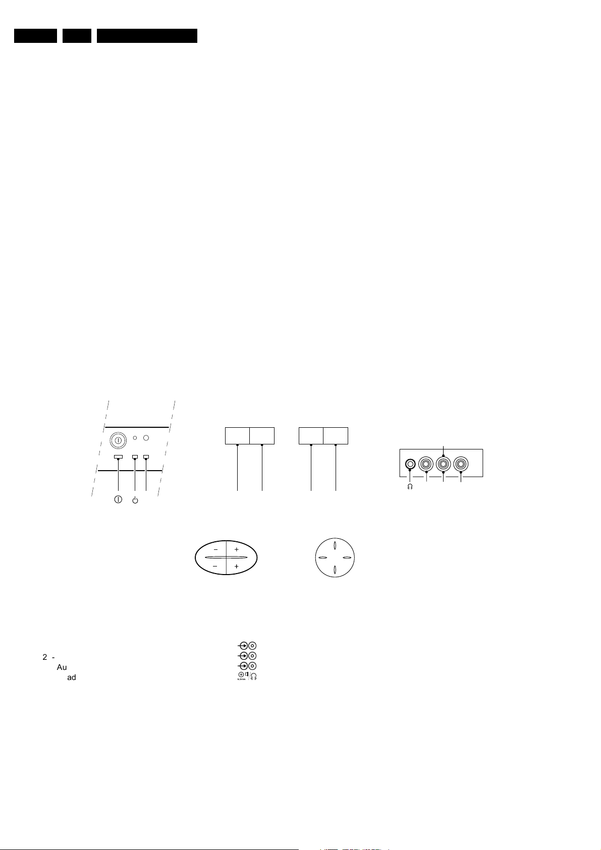
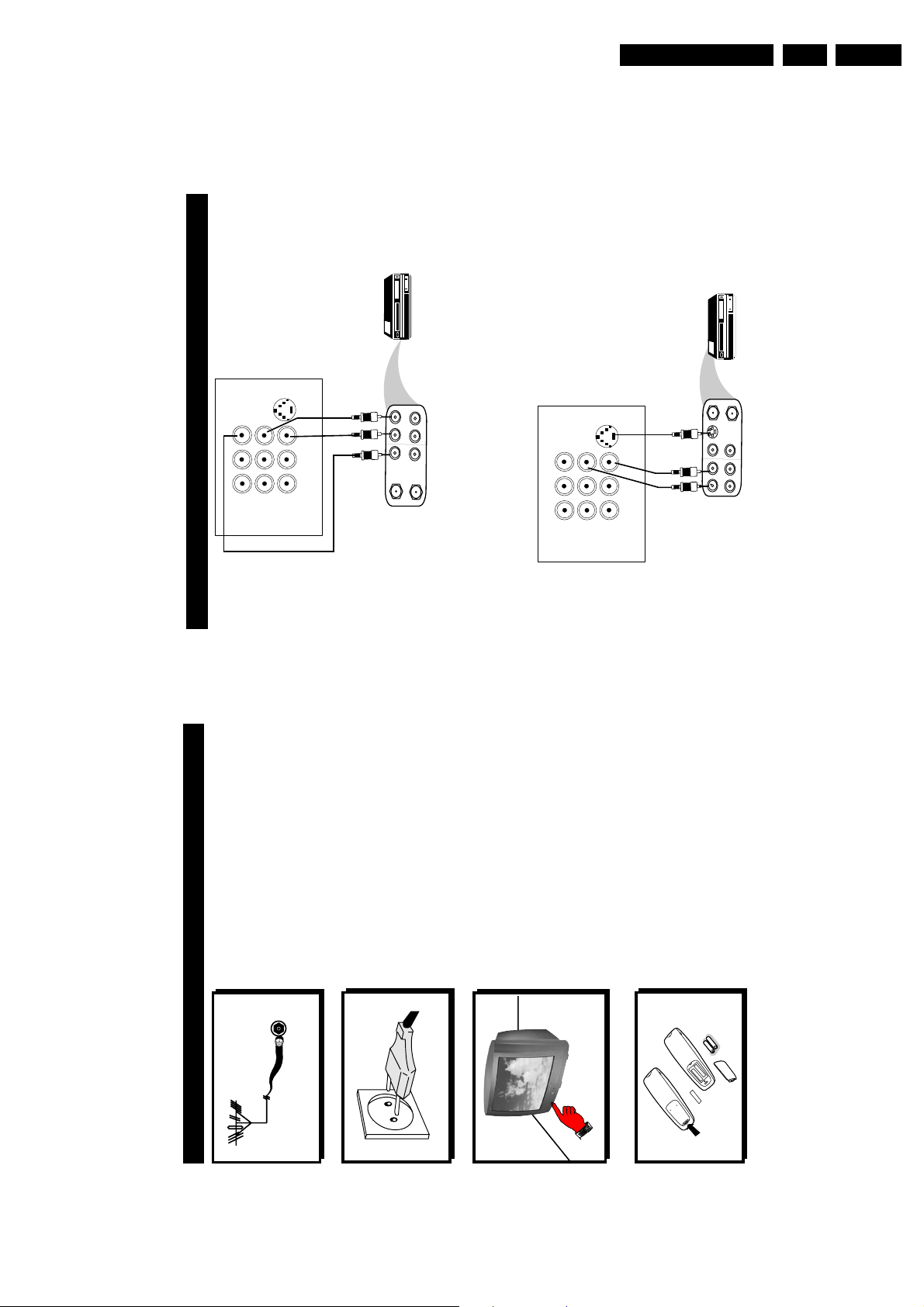
1.2 Connections
1.2.1 Front (or Side) Connections and Front (or Top) Control
A/V connections : NTSC 3.58, 4.43
: FM-stereo
:PAL 60
Channel selections : 100 channels
: U, V, S, H
Aerial input : 75 W, IEC-type
1.1.2 Miscellaneous
Audio output : 1 x 4 W or,
: 2 x 3 W or,
: 2 x 5 W + 10 W (sw)
+ 2 x 3 W
Mains voltage : 90 - 276 V or,
: 150 - 276 V
Mains frequency : 50 Hz or,
:60 Hz
Ambient temperature : + 5 to + 45 deg. C
Maximum humidity : 90 %
Power consumption : 36 W (14”) to
:52 W (21”)
Standby Power consumption : < 3 W
IR
RED
A/V In (if present)
1 - Video CVBS (1 Vpp / 75 W)
2 - Audio L (0.2 Vrms / 10 kW)
3 - Audio R (0.2 Vrms / 10 kW)
4 - Headphone (8 - 600 W / 4 mW)
V- C+C-V+
- VOLUME +
- PROGRAM +
Figure 1-1
C+C-V+V-
P+
P-
Mono
R
L
Video
Audio
V+V-
CL 16532016_020.eps
220501
Page 3
Technical Specifications, Connections and Chassis Overview
GB 3L01.2A 1.
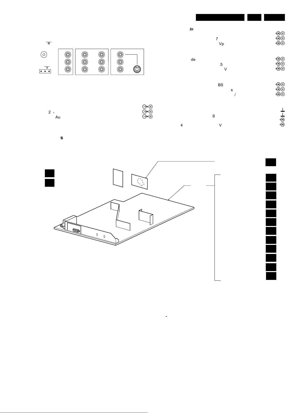
1.2.2 Rear Connections
75 Ohm
FM
MONITOR
OUT
V
L
R
Y
U
V
Figure 1-2
Monitor Out
1 - Video CVBS (1 Vpp / 75 W)
2 - Audio L (0.5 Vrms / 1 kW)
3 - Audio R (0.5 Vrms / 1 kW)
1.3 Chassis Overview
AV1
IN
YUV In (if present)
1 - Y 0.7 Vpp / 75 W
2 - U 0.7 Vpp / 75 W
AV2
IN
V
L
R
V
L
R SVHS
CL 16532008_005.eps
120601
3 - V 0.7 Vpp / 75 W
AV1 In
4 - Video CVBS (1 Vpp / 75 W)
5 - Audio L (0.5 Vrms / 10 kW)
6 - Audio R (0.5 Vrms / 10 kW)
AV2 In
1 - Video CVBS (1 Vpp / 75 W)
2 - Audio L (0.5 Vrms / 10 kW)
3 - Audio R (0.5 Vrms / 10 kW)
AV2 In (SVHS)
1 - gnd
2 - gnd
3 - Y 1 Vpp / 75 W
4 - C 0.3 Vpp / 75 W
CRT PANEL
B
SIDE AV PANEL + HEADPHONE
E1
SIDE AV PANEL
E
MAIN
CHASSIS
PANEL
POWER SUPPLY
LINE DEFLECTION
FRAME DEFLECTION
TUNER IF
VIDEO + SOUND IF
SYNCHRONISATION
CONTROL (µP)
AUDIO AMPLIFIER
NICAM + 2CS +
BTSC DECODER
A/V SWITCHING
HEADPHONE + FR. CONTROL
REAR I/O CINCH
CL 16532008_043.eps
A1
A2
A3
A4
A5
A6
A7
A8
A9
A10
A12
A13
240801
Figure 1-3
Page 4
GB 4 L01.2A2.
Safety & Maintenance Instructions, Warnings, and Notes
2. Safety & Maintenance Instructions, Warnings, and Notes
2.1 Safety Instructions For Repairs
Safety regulations require that during a repair:
• Due to the ‘hot’ parts of this chassis, the set must be
connected to the AC power via an isolation transformer.
• Safety components, indicated by the symbol
be replaced by components identical to the original ones.
• When replacing the CRT, safety goggles must be worn.
Safety regulations require that after a repair, the set must be
returned in its original condition. Pay particular attention to
the following points:
• General repair instruction: as a strict precaution, we
advise you to re-solder the solder connections through
which the horizontal deflection current is flowing, in
particular:
– all pins of the line output transformer (LOT)
– fly-back capacitor(s)
– S-correction capacitor(s)
– line output transistor
– pins of the connector with wires to the deflection coil
– other components through which the deflection
current flows.
Note: This re-soldering is advised to prevent bad connections
due to metal fatigue in solder connections and is therefore
only necessary for television sets more than two years old.
• Route the wire trees and EHT cable correctly and secure
them with the mounted cable clamps.
• Check the insulation of the AC power cord for external
damage.
• Check the strain relief of the AC power cord for proper
function, to prevent the cord from touching the CRT, hot
components, or heat sinks.
• Check the electrical DC resistance between the AC plug
and the secondary side (only for sets that have an
isolated power supply). Do this as follows:
1. Unplug the AC power cord and connect a wire
between the two pins of the AC plug.
2. Turn on the main power switch (keep the AC power
cord unplugged!).
3. Measure the resistance value between the pins of
the AC plug and the metal shielding of the tuner or
the aerial connection of the set. The reading should
be between 4.5 MW and 12 MW.
4. Switch the TV OFF and remove the wire between the
two pins of the AC plug.
• Check the cabinet for defects, to prevent the possibility of
the customer touching any internal parts.
2.2 Maintenance Instructions
It is recommended to have a maintenance inspection carried
out by qualified service personnel. The interval depends on
the usage conditions:
• When the set is used under normal circumstances, for
example in a living room, the recommended interval is
three to five years.
• When the set is used in an environment with higher dust,
grease or moisture levels, for example in a kitchen, the
recommended interval is one year.
• The maintenance inspection includes the following
actions:
1. Perform the 'general repair instruction' noted above.
2. Clean the power supply and deflection circuitry on
the chassis.
3. Clean the picture tube panel and the neck of the
picture tube.
, should
2.3 Warnings
• In order to prevent damage to ICs and transistors, avoid
all high voltage flashovers. In order to prevent damage to
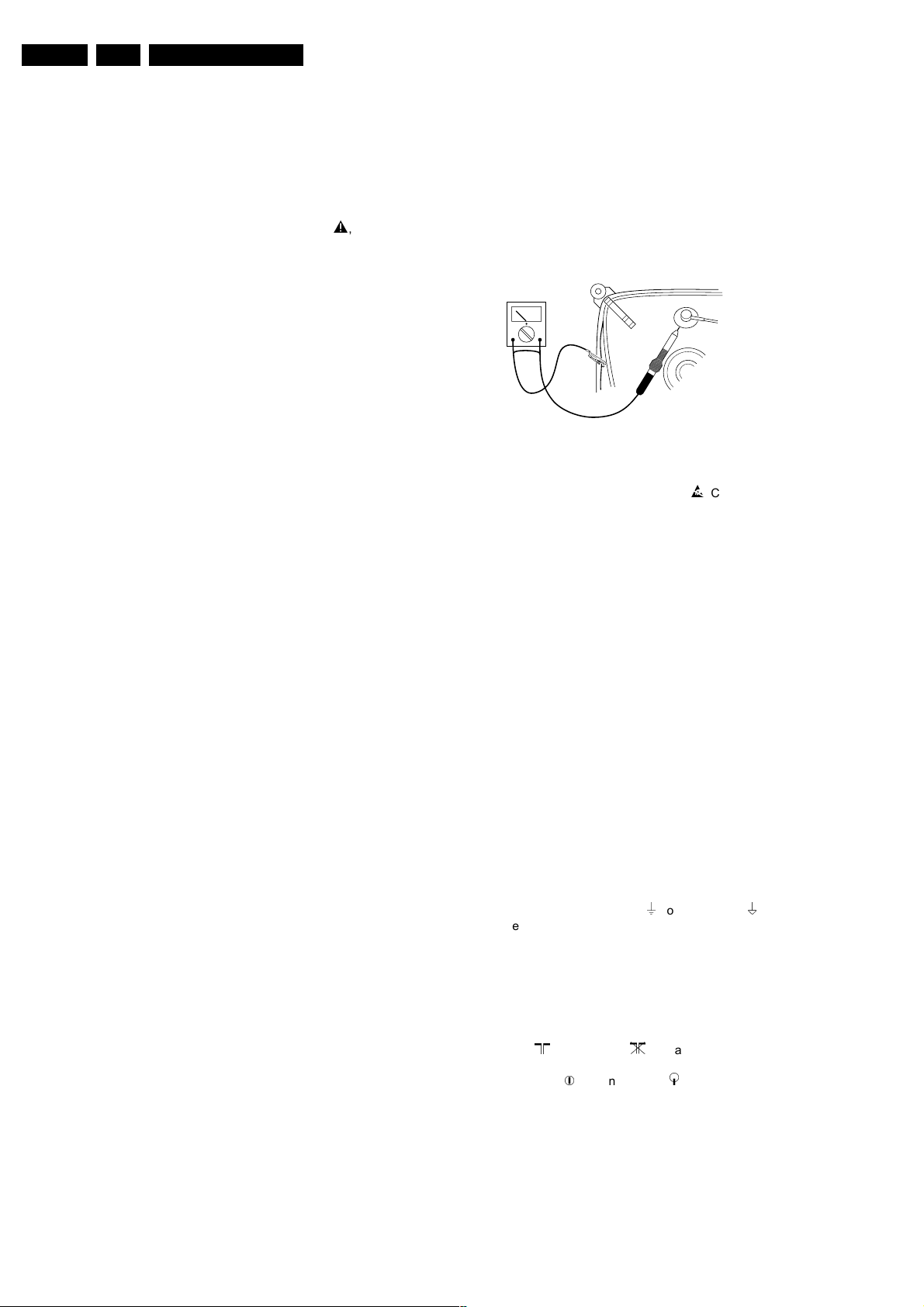
the picture tube, use the method shown in Fig. 2-1, to
discharge the picture tube. Use a high voltage probe and
a multi-meter (position VDC). Discharge until the meter
reading is 0 V (after approx. 30 s).
V
CL 26532098/042
140792
Figure 2-1
• All ICs and many other semiconductors are susceptible
to electrostatic discharges (ESD)
during repair can reduce life drastically. When repairing,
make sure that you are connected with the same
potential as the mass of the set by a wristband with
resistance. Keep components and tools also at this
potential. Available ESD protection equipment:
– Complete kit ESD3 (small tablemat, wristband,
connection box, extension cable, and ground cable)
4822 310 10671.
– Wristband tester 4822 344 13999.
• Together with the deflection unit and any multi-pole unit,
flat square picture tubes form an integrated unit. The
deflection and the multi-pole units are set optimally at the
factory. Adjustment of this unit during repair is therefore
not recommended.
• Be careful during measurements in the high voltage
section and on the picture tube.
• Never replace modules or other components while the
unit is switched ON.
• When you align the set, use plastic rather than metal
tools. This will prevent any short circuits and the danger
of a circuit becoming unstable.
. Careless handling
2.4 Notes
• Measure the voltages and waveforms with regard to the
chassis (= tuner) ground (
depending on the area of circuitry being tested.
• The voltages and waveforms shown in the diagrams are
indicative. Measure them in the Service Default Mode
(see chapter 5) with a color bar signal and stereo sound
(L: 3 kHz, R: 1 kHz unless stated otherwise) and picture
carrier at 475.25 MHz (PAL) or 61.25 MHz (NTSC,
channel 3).
• Where necessary, measure the waveforms and voltages
) and without () aerial signal. Measure the
with (
voltages in the power supply section both in normal
operation (
indicated by means of the appropriate symbols.
• The picture tube panel has printed spark gaps. Each
spark gap is connected between an electrode of the
picture tube and the Aquadag coating.
• The semiconductors indicated in the circuit diagram and
in the parts lists are completely interchangeable per
position with the semiconductors in the unit, irrespective
of the type indication on these semiconductors.
) and in standby (). These values are
), or hot ground (),
Page 5
3. Directions for Use
6
You can view the playback of VCR tapes (Video Disc players, camcorders, etc.) by using the AUDIO
and VIDEO INPUT sockets on the rear of the TV.
– Connect the VIDEO and AUDIO IN sockets on the rear of the TV to the AUDIO and
VIDEO OUT sockets on the VCR.
The S-Video connection on the rear of the TV is used for the playback of S-VHS VCR tapes, Video Discs,
Video Games or Compact Disc-Interactive (cd-i) discs. Better picture detail and clarity is possible with
the S-Video playback as compared to the picture from a normal antenna (RF) connection.
– Connect the S-VIDEO socket on the rear of the TV to the S-VHS OUT socket on a
S-VHS VCR.
– Connect the AUDIO IN sockets from the rear of the TV to the AUDIO OUT sockets
on the VCR. Note : You need not connect the VIDEO IN socket of the TV if S-VIDEO IN
socket is connected.
C
ONNECTING
THE
A
UDIO
/V
IDEO
S
OCKETS
(P
LAYBACK
)
ANTENNA
OUT
IN
OUT
IN
AUDIO RL
VIDEO
IN
OUT
L
R
S-VIDEO
VIDEO
AUDIO
AV1
in
AV2
in
Monitor
out
Back of VCR
VCR (Equipped with
Video and Audio
Output sockets
AV sockets on
rear of TV
ANTENNA
OUT
IN
OUT
IN
AUDIO RL VIDEO
IN
OUT
OUT
S-VIDEO
L
R
S-VIDEO
VIDEO
AUDIO
AV1
in
AV2
in
Monitor
out
Back of S-VHS VCR
AV sockets on
rear of TV
Directions for Use
GB 5L01.2A 3.
¬¬
¬¬
¬
compartment.
on the backcover.
Antenna Connection
• Connect the aerial plug to the antenna socket
• Insert the mains plug into the wall socket.
75 Ω
g
REPARATION
P
the rear of the TV set
Note : This diagram is not representative of the
Mains Connection
• For correct mains voltage, refer to type sticker at
• Consult your dealer if mains supply is different.
actual plug and socket.
Switching on the Set
• Press the main power button to switch on/
control to switch on set.
off the TV.
press the Powe r button on the remote
• If the set is on standby (indicator is red),
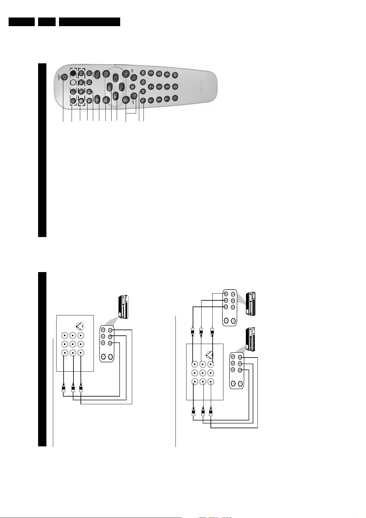
Using the Remote Control
• Insert the correct type of batteries into the
direction.
• Ensure the batteries are placed in the right
–
+
5
Page 6
GB 6 L01.2A3.
8
& Power button
– Switch set off temporarily to standby mode.
(The red light indicator lights up when the set
is on standby mode).
– To switch on set from standby mode, press
Channel +/– , Digit (0 -9) or Power button.
é Teletext Colour/Personal Zapping buttons
– In teletext mode, the colour buttons allow you to
access directly an item or corresponding pages.
– As Personal Zapping buttons, you can surf up to
10 personal channels for each button. For detailed
description of functions, refer to section on
“Personal Zapping ”.
“ Teletext buttons
Allows you to access teletext information. For
detailed description of functions, refer to section
on “Using the Teletext”
‘ Smiley button
Allows to add and store your personal preference
channels in your Personal Preference list. For
detailed description of functions, refer to section
on “Using your Personal Zapping feature”.
( Timer Button
Allows you to set the clock to switch to another
channel at a specified time while you are watching
another channel or when the set is on standby mode.
§ Smart Sound Button
Press the Smart Sound button repeatedly to
access 4 different types of sound settings and
choose your desired setting.
è Menu Button
Displays the main menu. Also exits menu from screen.
! Cursor Up Button
Allows you to select the next item on the menu.
ç Cursor Left Button
Allows you to select the sub-menus and adjust the settings.
0 Volume + / – Button
Increases or decreases volume.
1
44
44
4
Allows you to switch from Stereo to Mono sound during
stereo transmission or to choose between language5or
language6during dual sound transmission.
2 A/CH(Alternate channel) Button
Allows you to change between the current
channel and the previous channel.
F
UNCTIONS
OF
R
EMOTE
C
ONTROL
&
“
(
§
ç
0‘1é2
!
è
Directions for Use
)
ECORDING
(R
OCKETS
S
IDEO
/V
UDIO
A
THE
ONNECTING
C
Connection for recording from the TV channel
AV sockets on
rear of TV
VIDEO
S-VIDEO
L
AUDIO
R
in
AV2
in
AV1
out
Monitor
VCR (Equipped
OUT
OUT
OUT
with Video and
Audio Input
sockets
R
IN
AUDIO
L
IN
VIDEO
IN
ANTENNA
Back of VCR
system instead of the VCR. For mono equipment, connect only the AUDIO L socket.
sockets on the rear of the TV.
– Connect the corresponding INPUT sockets of the VCR to the MONITOR OUTPUT
– To enhance the sound of your TV, connect the AUDIO L and R sockets to an external audio
Connection for recording from one VCR to another VCR
R
IN
OUT
AUDIO
L
IN
OUT
VIDEO
IN
OUT
ANTENNA
S-VIDEO
AV2
AV1
Monitor
R
L
AV sockets on rear of TV
VIDEO
AUDIO
R
OUT
AUDIO
L
in
OUT
VIDEO
in
out
OUT
ANTENNA
IN
IN
IN
VCR (Equipped
with Video and
Audio Output
sockets
VCR (Equipped
with Video and
Audio Input
sockets
7
Back of VCR
sockets at either AV1 or AV2
rear of the TV.
– Connect the sockets of the VCR which you wish to record from, to the corresponding
– Connect the sockets of the receiving VCR to the MONITOR OUTPUT sockets on the
Page 7
Directions for Use
10
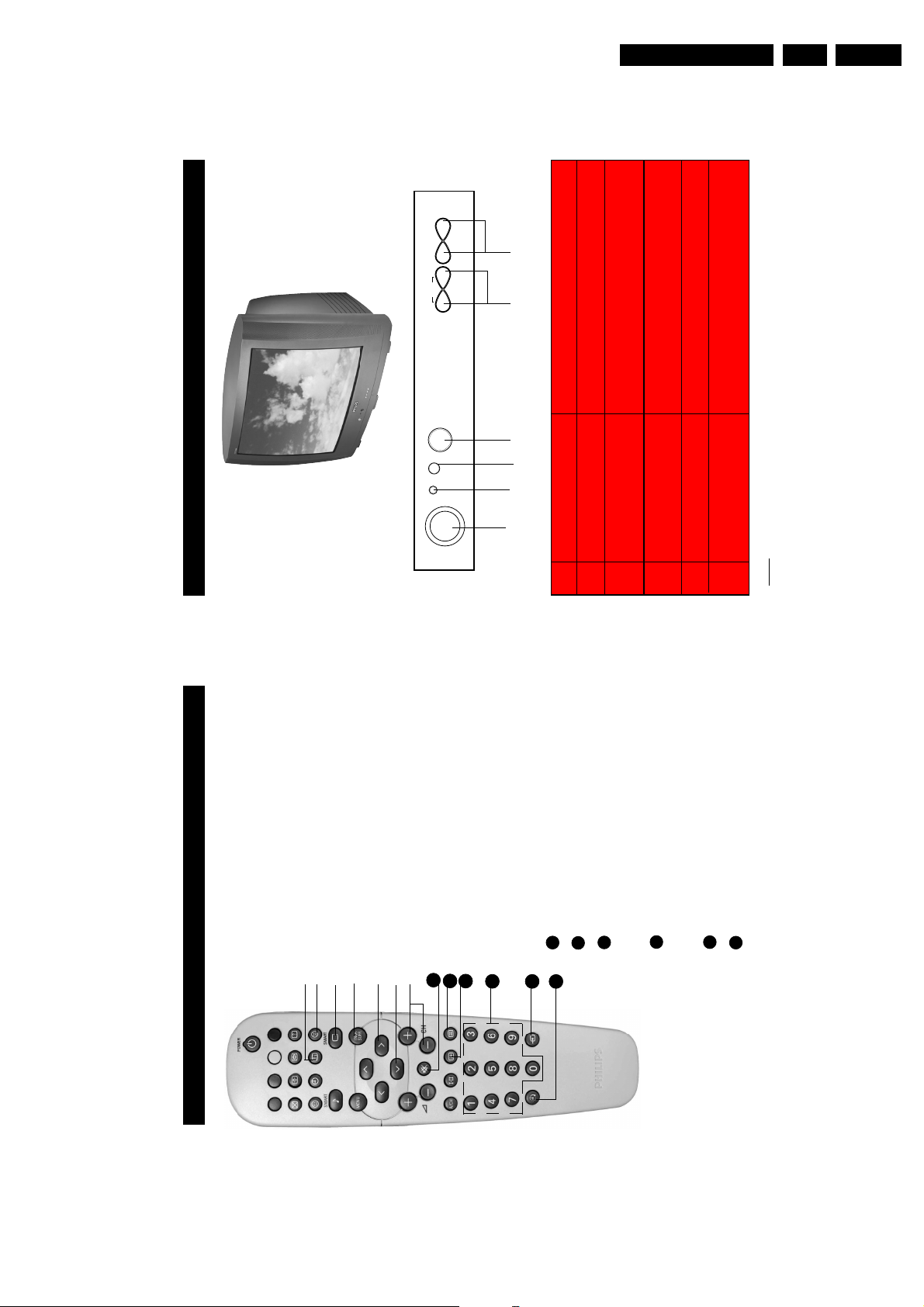
& Mains Power button Switch mains power on or off.
é Standby light indicator Indicate red light when standby mode is activated.
“ Remote Sensor Acts as a sensor for activating the controls of the
TV when remote control handset is aimed at it.
‘ Headphone socket Connect headphone jack to socket for personal
listening.
( Volume 8/9 buttons Adjust sound volume softer/louder.
§ Channel 7 / 6 buttons Select channel in descending/ascending order.
Note
• You can enter the main menu by pressing both the Volume 8 and 9 buttons at the
same time.
• Press the 7 or 6 button to select the next item on the menu.
• Press Volume 8 or 9 button to access sub-menu and adjust the settings.
é“ ‘ ( §
VOLUME
LK
˙
˝
˚
¸
CHANNEL
˚
¸
INSTALL /
MENU
FUNCTIONS
OF
TV
CONTROLS
➩
&
GB 7L01.2A 3.
ONTROL
C
EMOTE
R
OF
UNCTIONS
F
In teletext mode, press button to return to the
3 Main Index Button
main index page.
Allows to delete stored personal preference
4 Frownie button
channels in your Personal Preference list. For
detailed description of functions, refer to section on
“Personal Zapping ”.
5 Smart Picture Button
3
4
5
Press the Smart Picture button repeatedly to
access 5 different types of picture settings and
choose your desired setting.
6
7
when transmission is in stereo mode.
61Incredible Surround Button
– Allows you to select Incredible Surround sound
9
8
Allows you to access the sub-menus and adjust
the settings.
transmission is in mono mode.
– Allows you to select Spatial Sound when
71\Cursor Right Button
20
21
22
Allows you to select the next item on the menu.
Allows you to select channels in ascending or
descending order.
Mutes sound. To restore sound, press button again.
Refer to section on “Using the Teletext”
Allows you to display the current channel number.
It also allows to exit menu from the screen after
8 Cursor Down Button
9 Channel + / – Buttons
20 Mute Button
21 Teletext Button
22 OSD button
23
24
25
control adjustments.
Press to select a channel. For a 2-digit channel
23 Digit (0 -9) Buttons
Allows you to select the AV channels.
number, press the first digit and followed
immediately by the second digit.
Allows you to select a time period after which the
24 A/V Button
25 Sleeptimer Button
setwill switch to standby mode automatically.
9
Page 8
GB 8 L01.2A3.
12
A
UTOMATIC
T
UNING
OF
C
HANNELS
Automatic tuning of channels allows you to store each programme automatically.
Enter main menu.
Press button repeatedly until
Install is selected.
Enter install menu.
Select Auto Store.
Start automatic tuning of
channels.
When tuning is completed,
exit menu from screen.
¸
Main o
✔ Picture π Brightness
■
Sound Colour■Features Contrast
■
Install Sharpness
Colour Temp.
More...
œ
Main o
■
Picture Language
■
Sound Auto Store
■
Features Manual Store
✔ Install π Sort
Channel Edit
Name
œ
Install o
✔ Language π English
■
Auto Store
■
Manual store
■
Sort■Channel Edit
■
Name
œ
˙
¸
Install o
■
Language
✔ Auto Store π
■
Manual store
■
Sort■Channel Edit
■
Name
œ
˙
Auto Store
■
Channel 1■TV 142 MHz
♦♦♦♦♦♦♦♦♦♦♦♦♦♦π♦♦♦♦♦♦♦♦♦♦♦♦♦♦♦♦
Install o
■
Language
✔ Auto Store π
■
Manual store
■
Sort■Channel Edit
■
Name
œ
MENU
Step
Result on TV Screen
Press button
m
Directions for Use
ANGUAGE
L
ENU
M
THE
ELECTING
S
Operating instructions generally explains the operation of the TV
Result on TV Screen
Press button
set using the buttons on the remote control unless otherwise stated.
Please read the following instructions carefully and follow the steps
as shown to familiarise yourself with the installations and all features
available in your set.
desired language.
Step
The Language feature allows you to set the TV’s on-screen menu to be shown in your
Main o
Enter main menu.
MENU
Colour Temp.
Sound Colour■Features Contrast
Install Sharpness
✔ Picture π Brightness
■
■
More...
œ
Channel Edit
Picture Language
Sound Auto Store
Features Manual Store
Main o
■
■
■
✔ Install π Sort
Select Install.
¸
Name
œ
Auto Store
Install o
✔ Language English π
■
Enter the Install menu.
˙
Manual store
■
œ
Sort■Channel Edit
Name
■
■
Press button repeatedly to cycle
through the language list and
select the language of your choice.
˙
Exit menu from screen.
m
UNING
T
11
UTOMATIC
A
Page 9
Directions for Use
14
C
HANNELS
M
ANUAL
T
UNING
OF
C
HANNELS
¸
Manual Store o
■
Colour System
■
Sound System
■
Search
✔
Channel No. 2 π
■
Fine Tune
■
Store
œ
Manual Storeo
■
System■Search■Channel No.
■
Fine Tune
✔
Store Store?π
œ
˙
¸
9
10
11
Manual Storeo
■
System■Search■Channel No.
■
Fine Tune
✔
Store Stored
œ
12
˙
Start manual searching. Searching
stops once a transmitting signal is
found.
Select Channel No.
Key in the channel number.
Press button repeatedly until
Store is selected.
Store tuned channel.
Note : If you want to
continue searching for
another transmitting
channel, repeat steps
7 to 11.
Exit menu from screen.
Manual Store o
■
Colour System
■
Sound System
✔
Search 128 MHz π
■
Channel No.
■
Fine Tune
■
Store
œ
Step
Result on TV Screen
Press button
5
1
3
2
4
6
7
9
8
0
m
GB 9L01.2A 3.
HANNELS
C
OF
UNING
T
ANUAL
M
Manual tuning of channels allows you to select your preferred channel number for every
available programme.
Main o
Enter main menu.
Press button
Step Result on TV Screen
Colour Temp.
Sound Colour■Features Contrast
Install Sharpness
✔ Picture π Brightness
■
■
MENU
More...
œ
Main o
Picture Language
Sound Auto Store
Features Manual Store
■
■
■
✔ Install π Sort
Press button repeatedly until
Install is selected.
¸
Channel Edit
Name
œ
œ
Auto Store
Manual Store
Sort■Channel Edit
✔ Language π English
■
■
Name
■
■
Install o
Enter install menu.
˙
Manual Store π Search
Language Colour System
Auto Store Sound System
Sort Channel No.
Channel Edit Fine Tune
Install o
■
■
✔
■
■
Press button repeatedly until
Manual Store is selected.
¸
œ
Name Store
■
Search 79 MHz π
Colour System
Sound System
Channel No.
Fine Tune
Manual Store o
■
■
✔
■
■
Enter manual store menu.
Press button repeatedly until
˙
¸
œ
Store
■
OF
UNING
T
ANUAL
M
Search is selected.
13
Page 10
GB 10 L01.2A3.
16
F
INE
T
UNING
OF
C
HANNELS
This feature allows you to adjust picture reception in areas of weak reception.
Enter main menu.
Press button repeatedly until
Install is selected.
Enter install menu.
Press button repeatedly until
Manual Store is selected.
Enter manual store menu.
Press button repeatedly until
Fine Tune is selected.
Fine tune until the best reception
is obtained.
Select Store.
Store last fine-tuned status.
Exit menu from screen.
Main o
✔ Picture π Brightness
■
Sound Color■Features Contrast
■
Install Sharpness
Tint
More...
œ
Main o
■
Picture Language
■
Sound Auto Store
■
Features Manual Store
✔ Install π Sort
Channel Edit
Name
œ
¸
˙
¸
˙
¸
˙
¸
˙
9
Install o
■
Language Colour System
■
Auto Store Sound System
✔
Manual Store π Search
■
Sort Channel No.
■
Channel Edit Fine Tune
■
Name Store
œ
Manual Storeo
■
Colour System
■
Sound System
■
Search■Channel No.
✓ Fine Tune
p
❘❘❘❘❘❘❘❘❘❘❘
❘❘
❘❘❘❘❘❘❘❘❘❘❘
π
■
Store
œ
Manual Storeo
■
Colour System
■
Sound System
■
Search■Channel No.
✓ Fine Tune
p
❘❘❘❘❘❘❘❘❘❘❘❘❘❘❘❘❘❘
❘❘
❘❘❘❘
π
■
Store
œ
Manual Storeo
■
System■Search■Channel No.
■
Fine Tune
✔
Store Stored
œ
10
Step
Press button
Result on TV Screen
MENU
m
or
˝
Directions for Use
YSTEM
S
OUND
/S
OLOUR
C
THE
ELECTING
S
is selected, the respective colour and sound system will be automatically selected according
to the transmission system. Note : Select your desired colour and sound system manually if
This feature allows you to select your desired Colour and Sound system. If Auto
Result on TV Screen
Press button
Step
reception is poor at Auto mode.
Colour System Auto π
Sound System
Search■Channel No.
Manual Store o
✔
■
■
Repeat step 1 Colour System is selected.
to step 5 as in
“Manual Tuning
œ
Fine Tune
Store
■
■
of TV Channels”
œ
Colour System PAL π
Sound System
Search■Channel No.
Fine Tune
Manual Store o
Select the desired colour
˝
Store
✔
■
■
■
■
NTSC 3.58, NTSC 4.43
or SECAM).
system (Auto, PA L ,
˙
or
Colour System
Sound System
Manual Store o
■
Press button repeatedly
until STORE is selected.
¸
œ
Search■Channel No.
Fine Tune
Store Stored
■
■
■
✔
Store selected system.
˙
Sound System Auto π
Colour System
Search■Channel No.
Manual Store o
■
✔
■
Proceed to select Sound
System.
or
¸
˚
9
œ
Fine Tune
Store
■
■
Manual Store o
Select the desired sound
˝
Sound System DK π
Colour System
Search■Channel No.
Fine Tune
Store
■
✔
■
■
■
system (Auto, BG, I,
DK or M.
˙
or
10
œ
Colour System
Sound System
Manual Store o
■
Press button repeatedly
¸
11
œ
Search■Channel No.
Fine Tune
Store Stored
■
■
■
✔
until STORE is selected.
Store selected system.
˙
12
15
Exit menu from screen.
m
13
Page 11
18
EDITING OF CHANNELS
This feature allows you to skip or edit channels which have bad or weak TV signal or channels
that you do not watch often. Note : Once a channel is skipped, you cannot have access to it by
theCH (Channel) + or – button. You can only have access to the channel by the Digit (0 -9)
buttons.
Main o
■
Picture Language
■
Sound Auto Store
■
Features Manual Store
✔ Install π Sort
Channel Edit
Name
œ
Install o
■
Language Channel No.
■
Auto Store Skipped■Manual Store
■
Sort
✔
Channel Edit π
■
Name
œ
Enter main menu.
Press button repeatedly until
Install is selected.
Enter install menu.
Press button repeatedly until
Channel Edit is selected.
Enter Channel Edit menu.
Key in the channel number to be
skipped.
Select Skipped.
Select On to skip channel.
Exit menu from screen.
Channel Edit o
✔
Channel No. 2 π
■
Skipped
œ
Channel Edit o
■
Channel No.
✔
Skipped On
œ
9
H
OW
TO
R
ESTORE
S
KIPPED
C
HANNELS
• Repeat Steps 1 to 5 as in”Editing of Channels”.
• Key in the channel number to be restored by the
Digit (0 - 9) button.
• Select Skipped by the Cursor Dow button.
• Select Off to restore channel by the Cursor Right button.
• Exit menu from screen by the OSD button.
Channel Edit o
■
Channel No.
✔
Skipped Off
œ
Step
Result on TV Screen
Press button
MENU
m
5
1
3
2
4
6
7
9
8
0
¸
˙
¸
˙
¸
˙
Directions for Use
GB 11L01.2A 3.
HANNELS
C
OF
ORTING
S
This feature rearranges channel numbers.
Picture Language
Sound Auto Store
Main o
■
■
Enter main menu.
MENU
Press button
Step Result on TV Screen
Channel Edit
Name
œ
Features Manual Store
■
✔ Install π Sort
Press button repeatedly until
Install is selected.
¸
Language 000■Auto Store 001■Manual Store 002✔Sort π 003■Channel Edit 004■Name 005
Install o
■
Enter install menu.
Press button repeatedly until
Sort is selected.
˙
¸
œ
Language 000■Auto Store 001■Manual Store 002 π
Install o
■
Enter sort mode.
˙
Sort π 003
Channel Edit 004■Name 005
✔
■
Select the channel number you want
to change from (e.g. 002).
or
¸
œ
Language 000■Auto Store 001■Manual Store 002 p✔Sort π 003■Channel Edit 004■Name 005
Install o
■
Confirm selection.
˙
˚
œ
Language 000■Auto Store 001■Manual Store 002✔Sort π 003■Channel Edit 004■Name 005 p
Install o
■
Select the channel number you want
¸
to change to (e.g. 005).
œ
Language 000■Auto Store 001■Manual Store 002
Install o
■
Confirm selection.
The change is done.
Note : Channel numbers 5, 4 and 3
˝
9
œ
Sort π 003
Channel Edit 004■Name 005 π
✔
■
17
will move upwards accordingly. that
is, Channel 5 will move up to Channel
4, Channel 4 to 3 and Channel 3 to 2.
Exit menu from screen.
m
10
Page 12
GB 12 L01.2A3.
Result on TV Screen
Directions for Use
ICTURE
TV P
THE
DJUSTING
A
The picture menu allows you to make adjustments to the picture.
Main o
✔ Picture π Brightness
Display the main menu on screen.
MENU
Press button
Step
Colour Temp
More...
Sound Colour■Features Contrast
Install Sharpness
■
■
œ
Picture o
Enter Picture menu.
59π
❘❘❘❘❘❘❘❘❘❘❘
❘
❘❘❘❘❘❘❘❘❘❘❘
Colour■Contrast
✔ Brightnessp
■
Select item.
˙
œ
Sharpness
Colour Temp
NR
■
■
■
or
¸
˚
59π
❘❘❘❘❘❘❘❘❘❘❘
❘
❘❘❘❘❘❘❘❘❘❘❘
Picture o
✔ Colour p
Adjust level or select desired
Contrast
Sharpness
Colour Temp
■
■
■
setting.
or
˝
œ
Contrast +
■NR■
Exit menu from screen.
˙
m
Picture menu items Activities
Brightness Increase or decrease brightness level.
20
in picture.
Colour Increase or decrease color level.
Contrast Increase or decrease contrast level.
Sharpness Increase or decrease sharpness level to improve detail
picture) due to weak signal.
Color temperature Choose from 3 settings (Normal, Warm or Cool).
NR (Noise Reduction) Select “On” to reduce “noisy” picture (little dots on
for improved picture quality.
Contrast + Select “On” to allow you to optimise the total contrast
HANNELS
C
OF
AMING
N
This feature enables you to name or rename channels.
Enter main menu.
MENU
Press button
Step Result on TV Screen
Picture Language
Sound Auto Store
Main o
■
■
Press button repeatedly until
Channel Edit
Name
œ
Features Manual Store
■
✔ Install π Sort
Install is selected.
¸
œ
Name π 005
Language 000■Auto Store 001■Manual Store 002■Sort 003■Channel Edit 004
Install o
■
Enter install menu.
˙
Press button repeatedly until
Name is selected.
¸
✔
Language 000■Auto Store 001■Manual Store 002■Sort 003π■Channel Edit 004
Install o
■
Enter name mode.
Select the channel you want to
˙
˚
Name π 005
✔
œ
Language 000■Auto Store 001■Manual Store 002■Sort 003π■Channel Edit 004
Install o
■
Name π 005
✔
œ
19
name.
or
Move to first character slot.
¸
A cursor appears for you to start
the input of characters. Select the
character you want. Move to next
character slot by the Cursor Right
button and select the next character.
You can enter up to a
maximum of 5 characters.
˙
or
¸
˚
Exit menu from screen.
m
9
Page 13
Colour Temp.
Result on TV Screen
More...
œ
Directions for Use
œ
Display
œ
GB 13L01.2A 3.
œ
œ
IMER
T
THE
SING
U
Press button
The Timer feature allows you to set the timer to switch to another channel at a specified
time while you are watching another channel or when the TV is on standby mode.
Note : For the timer to function, the set must not be switched off. Once the set is switched
Step
off, the timer is disabled.
Sound Colour■Features Contrast
Install Sharpness
Main o
✔ Picture π Brightness
■
■
Display the main menu on screen.
MENU
Colour Temp.
More...
œ
Features π Format
Picture Timer■Sound Child Lock
Install
Main o
■
✔
■
Select Features.
¸
0π
❘❘❘❘❘❘❘❘❘❘❘
❘
Incr. Surround
Ultra Bass
❘❘❘❘❘❘❘❘❘❘❘
œ
Enter the Features menu.
˙
œ
Features o
✔ Timer π Time
Child Lock Start Time
Format Stop Time
Channel Activate
■
■
Enter Timer menu.
˙
Start Time
Timer o
✔ Time π 08:30
■
Key in the current time starting from
3
2
1
Stop Time
Channel■Activate
Display
■
■
■
and “stop time” will take reference
the hour follow by minute.
This is the time where the “start time”
6
9
5
0
8
7
4
from.
Timer o
■
Start Timeπ 10:30
Time
Stop Time
✔
■
Select Start Time.
¸
Channel■Activate
Display
■
■
Key in the time you want the
3
2
1
programme to be switched on.
6
9
5
0
8
7
4
22
OUND
TV S
THE
DUSTING
A
Display the main menu on screen.
Press button
Step Result on TV Screen
The sound menu allows you to make adjustments to the sound.
Sound Colour■Features Contrast
Main o
✔ Picture π Brightness
■
MENU
Install Sharpness
■
Picture Treble
Main o
■
Select Sound menu.
¸
Sound π Bass
Features Balance■Install AVL
✔
■
Bass■Balance■AVL■Incr. Surround
✔ Treble p
■
Select item.
˚
Ultra Bass
■
or
¸
Sound o
Enter Sound menu.
˙
Adjust level or select desired
˝
setting.
or
˙
Exit menu from screen.
m
Sound menu items Activities
Treble Increase or decrease high frequency level.
21
volume during commercial breaks or channel switching.
determined level should there be a sudden change in
Bass Increase or decrease low frequency level.
Balance Increase or decrease to adjust balance level.
AVL (Auto Volume Leveller) Select On to enable volume to remain at a pre-
Incredible Surround Select On to boost the effect of stereo sound.
Ultra Bass Select On to enjoy enhanced bass output.
Page 14
GB 14 L01.2A3.
Result on TV Screen
)
ODE
C
CCESS
(A
OCK
L
HILD
C
THE
CTIVATING
A
Picture Timer■Sound Child Lock
Main o
■
Display the main menu on screen.
Press button
MENU
Install
✔ Features π Format
■
Press button repeatedly until
Features is selected.
¸
Directions for Use
✔ Child Lock π
Select Child Lock.
¸
Format
■
œ
Enter Child Lock mode.
˙
œ
Timer
Features o
■
Enter the Features menu.
˙
Timer Access Code
Format Correct
Features o
■
✔ Child Lock π xxxx
■
Key in the 4-digit access code.
For the first time or if you have
3
2
1
œ
Timer New Code
Features o
■
forgotten the access code, enter
the universal access code 0711
twice. It will now prompt you to
key in a New Code.
6
9
5
0
8
7
4
œ
Format
✔ Child Lock π xxxx
■
Key in your preferred code (4-digit).
6
9
3
2
5
0
8
7
4
1
Timer Confirm Code
Format Confirmed
Features o
■
✔ Child Lock π xxxx
■
Child Lock o
Key in the new code the second
time to confirm code.
The Child Lock menu will now
6
9
3
2
5
0
8
7
4
1
006
007
œ
Lock Channel π 002■Change Code 003■Clear All 004■Lock All 005
■
appear. You can proceed to lock
œ
from screen.
channel (refer to section on
“Lock Channel”). If not, exit menu
m
24
The Child Lock feature allows you to lock channels to prevent your children from watching
IMER
T
THE
SING
U
programmes you deem undesirable.
Note : You can only have access to the locked channels via the remote control. Keep the
remote control out of reach so as to prevent your children from having access to it.
Result on TV Screen
Timer o
Select Stop Time.
Press button
¸
Step
Time■Start Time
Channel■Activate
Display
Stop Time π 12:30
■
✔
■
■
Key in the time you want the
3
2
1
œ
programme to be switched off.
6
9
5
8
7
4
9
Note : After you have exit menu from screen and you want to
enter the child lock menu again, you need to key the new
access code only once.
Time■Start Time
Stop Time
Channel
Timer o
■
■
■
Select Activate.
¸
Once
œ
Display
Activate π
✔
■
Activate timer. You can select
Once, Daily or Off.
˙
Timer o
■
¸
5
œ
Time■Start Time
Stop Time
Activate
Display
Channel π
Timer o
■
■
✔
■
■
Select Channel.
Key in the channel you want to
switch to.
6
9
3
0
2
5
0
¸
8
7
4
1
On
Time■Start Time
Stop Time
Channel■Activate
Display π
■
■
✔
Select Display.
Select On mode if you want to
display the time on the TV screen.
˙
œ
23
Exit menu from screen.
Note : After the Stop Time is activated,
m
Powe r button.
the TV will go on standby mode. To
switch on set from standby mode, press
Channel +/–, Digit (0 -9) or
Step
9
10
11
12
13
14
15
Page 15
Directions for Use
Result on TV Screen
006
)
007
œ
006
007 π
œ
006 π
007
œ
006 πF007
œ
GB 15L01.2A 3.
HANNEL
C
OCK
(L
OCK
L
HILD
C
THE
Press button
CTIVATING
A
Step
Change Code 003■Clear All 004■Lock All 005
Child Lock o
✔ Lock Channel π 002
■
The Child Lock menu will
now appear. You can proceed
to lock channel.
CCESS
Lock (A
)”
HILD
ODE
Repeat Steps 1 to 8 as
in “C
C
Child Lock o
✔ Lock Channel π 002
Enter lock channel mode.
˙
9
Change Code 003■Clear All 004■Lock All 005
■
Change Code 003■Clear All 004■Lock All 005
Child Lock o
✔ Lock Channel π 002
■
Select the channel you want
to lock.
or
˚
10
Change Code 003■Clear All 004■Lock All 005
Child Lock o
✔ Lock Channel π 002
■
26
Activate blocking of channel.
A keylock symbol will appear
beside the channel number
indicating that it is locked.
Note : To lock more than one
channel, repeat Steps 10 to 11
before exiting menu from
screen.
Exit menu from screen.
¸
˙
11
m
12
006
007
Result on TV Screen
œ
Change Code 003■Clear All 004■Lock All 005
Child Lock o
✔ Lock Channel π 002
■
Lock Channel New Code
Child Lock o
■
Clear All
Lock All
✔ Change Code π ----
■
■
œ
Lock Channel New Code
Child Lock o
■
Clear All
Lock All
✔ Change Code π xxxx
■
■
œ
Lock Channel Confirm Code
Child Lock o
■
Clear All Confirmed
Lock All
✔ Change Code π xxxx
■
■
œ
25
code.
The Child Lock menu will
now appear. You can proceed
to change
THE
Repeat Steps 1 to 8 as
CTIVATING
in “A
OCK
L
HILD
C
)”
ODE
C
CCESS
(A
Press button
ACTIVATING THE CHILD LOCK (CHANGE CODE)
Step
Note : You need to key the access code only once.
Select Change Code.
Enter change code mode.
˙
¸
9
10
Key in your preferred code
(4-digit).
6
9
3
2
5
0
8
7
4
1
11
Key in the new code the
second time to confirm
code.
6
9
3
2
5
0
8
7
4
1
12
Exit menu from screen.
m
13
Page 16
GB 16 L01.2A3.
➩
Result on TV Screen
ORMAT
F
Picture Timer■Sound Child Lock
Install
Main o
■
✔ Features π Format
■
Directions for Use
œ
Timer■Child Lock
Features o
■
✔ Format 4:3 π
œ
Timer■Child Lock
Features o
■
✔ Format 4:3 Expand π
œ
➩
➩
CREEN
S
THE
SING
U
You can have a choice of two formats for your viewing pleasure, namely : - 4:3 mode and the
)
LL
A
OCK
(L
OCK
L
HILD
C
THE
EXPAND 4:3 mode through the FORMAT menu.
Result on TV Screen
Display the main menu on screen.
MENU
Press button
Step
Change Code 003■Clear All 004■Lock All 005
Child Lock o
✔ Lock Channel π 002
■
The Child Lock menu will
now appear. You can proceed
to lock all channels.
Press button repeatedly until
Features is selected.
¸
006
007
œ
Enter the Features menu.
Press button repeatedly umtil
˙
¸
Lock Channel
Change Code
Clear All
Lock All π On
Child Lock o
■
■
■
■
Select Lock All.
Select the On option to
lock all channels.
Format is selected.
œ
Press the button repeatedly to
˙
Exit menu from screen.
cycle through the different formats
(4:3 or Expand 4:3) or and select
your desired format.
)
LL
A
LEAR
(C
OCK
L
HILD
C
THE
m
Exit menu from screen.
Result on TV Screen
4:3 format
When to use the Screen Formats
Select the 4:3 format if you want to
006
Change Code 003■Clear All 004■Lock All 005
Child Lock o
✔ Lock Channel π 002
■
The Child Lock menu will
now appear. You can proceed
to clear all channels.
display the 4:3 picture using the full
surface of the screen.
Expand 4:3 format
007
œ
Lock Channel
Child Lock o
■
Select Clear All.
Select the Expand 4:3 format if you
want to expand movie images
recorded in the letterbox format.
When this format is selected, the
black horizontal bars at the top and
bottom are expanded thus filling
up the entire TV screen.
œ
Change Code
Lock All
■
✔ Clear All π Off
■
Select the Off option to
unlock all channels.
Exit menu from screen.
28
27
CTIVATING
A
You can choose to lock all channels in the Lock All mode in the Child Lock menu.
CCESS
Press button
Lock (A
HILD
Step
Repeat Steps 1 to 8 as
in “C
)”
ODE
C
CCESS
˙
¸
m
CTIVATING
A
Press button
˙
¸
m
Lock (A
)”
9
10
11
To unlock channels that you have locked, enter the Child Lock menu and select the Off option
Clear All mode.
Step
Repeat Steps 1 to 8 as
HILD
in “C
ODE
C
9
10
11
Page 17
Directions for Use
30
SMART SOUND CONTROL
Whether you are watching a movie or video game, your TV has automatic sound control
settings matched to your current program source or content. The Smart Sound feature quickly
resets your TV’s sound controls of program for a number of different types of programs and
viewing conditions you may have in your home. Each Smart Sound setting is preset at the
factory to automatically adjust the TV’s Treble and Bass levels.
Press botton repeatedly to cycle through the 4 settings namely,
Personal, Voice, Music and Theatre and select your desired
sound setting.
Exit menu from screen.
Step
Press button
Personal
Voice
Music
Theatre
Definition of Sound Settings
Personal : Sound settings are set to your preference.
Voice : Emphasize high tone (treble boosted).
Music : Emphasize low tone (Bass boosted).
Theatre : Emphasize sensation to action.
(Bass and Treble boosted)
q
m
GB 17L01.2A 3.
ONTROL
C
ICTURE
P
MART
S
Whether you are watching a movie or video game, your TV has automatic video control
settings matched to your current program source or content. The Smart Picture feature quickly
resets your TV’s video controls of program for a number of different types of programs and
viewing conditions you may have in your home. Each Smart Picture setting is preset at the
factory to automatically adjust the TV’s Brightness, Colour, Picture and Sharpness levels.
Press botton repeatedly to cycle through the 5 settings namely,
`
Press button
Step
DVD/VCD, Rich, Natural, Soft and Personal and select
your desired picture setting.
Exit menu from screen.
m
DVD/VCD
Defintion of Picture Settings
DVD/VCD : For optimal picture setting, whenever
the source is connected to DVD/VCD
player, select DVD/VCD setting for AV
mode.
Rich
setting is the optimal setting when you
Rich : Emphasize very vibrant colours. This
Natural
are viewing TV programmes in a
brightly-lit room.
Natural : Emphasize original colours.
Soft
(Suitable for dimly-lit room condition and
givescinema-like effect when light is
switched off).
Soft : Emphasize “warm” colours.
Personal
29
Personal : Picture settings are set to your preference.
Page 18
GB 18 L01.2A3.
Directions for Use
Personal Notes:
29PT2152
PECIFICATIONS
S
PAL B/G
PAL D/K
PAL I
SECAM B/G
SECAM D/K
SECAM K1
34
Picture tube screen size 72 cm
Picture tube visible area 68 cm
Audio Output :
Speaker 2 x 5 W
TV System NTSC M
Set Dimensions :
Width 75.9 cm
Depth 51 cm
Height 57.5 cm
Net Weight of Set approximate 35 kg
Note
For Operating Voltage, Frequency, Power Consumption and Version Number, refer to the
type number at the rear of the set.
Page 19
4. Mechanical Instructions
Mechanical Instructions
GB 19L01.2A 4.
Index:
1. Rear Cover Removal
2. Service Position Main Panel
3. Side I/O Panel Removal
4. Rear Cover Mounting
Note: Figures can deviate slightly from the actual situation,
due to different set executions.
4.1 Rear Cover Removal
1. Remove all fixation screws of the rear cover.
2. Now pull the rear cover backward and remove it.
4.2 Service Position Main Panel
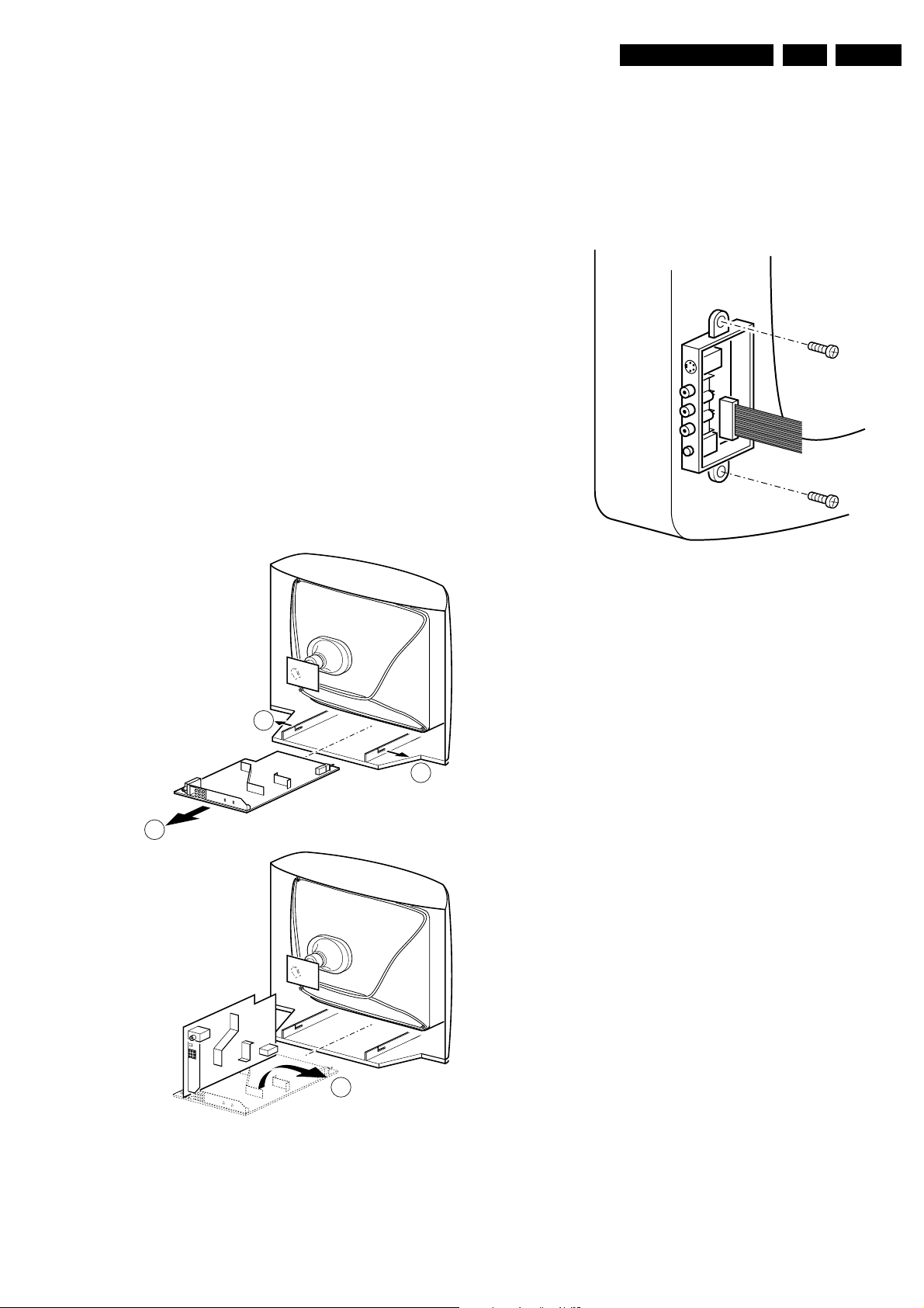
1. Disconnect the strain relief of the AC power cord.
2. Remove the main panel, by pushing the two center clips
outward [1]. At the same time pull the panel away from
the CRT [2].
3. Disconnect the degaussing coil by removing the cable
from (red) connector 0201.
4. Move the panel somewhat to the left and flip it 90
degrees [3], with the components towards the CRT.
4.3 Side I/O Panel Removal
1. Remove the complete Side I/O assembly after
unscrewing the 2 fixation screws [1].
2. Release the two fixation clamps [2] and lift the board out
of the bracket.
CL 06532012_004.eps
030200
Figure 4-2
4.4 Rear Cover Mounting
Before you mount the rear cover, perform the following
checks:
1
1
2
A
1. Check whether the mains cord is mounted correctly in its
guiding brackets.
2. Replace the strain relief of the AC power cord into the
cabinet.
3. Check whether all cables are replaced in their original
position.
B
Figure 4-1
3
CL 16532016_006.eps
220501
Page 20
GB 20 L01.2A5.
Service Modes, Error Codes and Fault Finding
5. Service Modes, Error Codes and Fault Finding
Index:
1. Test points.
2. Service Modes.
3. Problems and Solving Tips (related to CSM).
4. ComPair.
5. Error Codes.
6. The Blinking LED Procedure.
7. Protections.
8. Repair Tips.
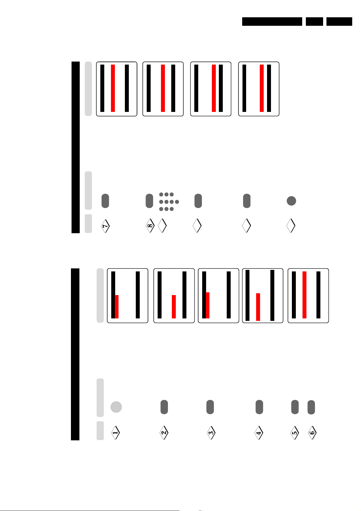
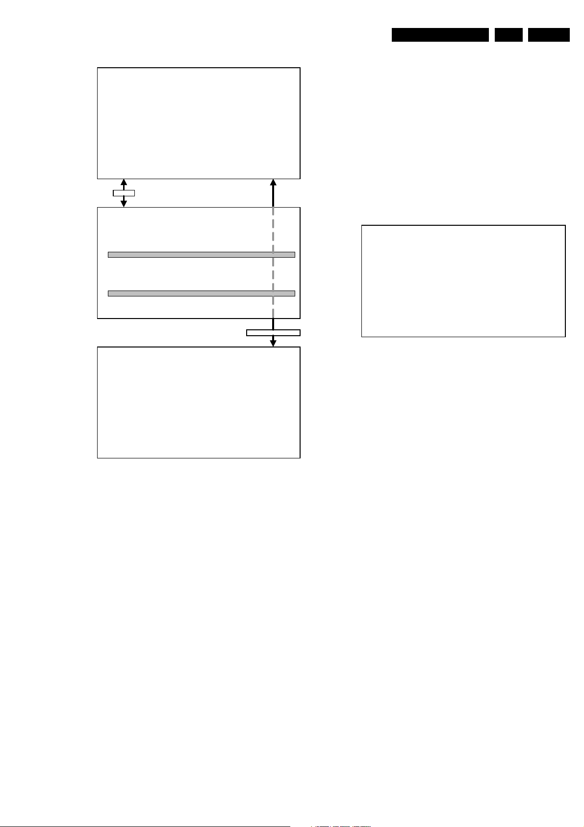
5.1 Test Points
The chassis is equipped with test points printed on the circuit
board assemblies. These test points refer to the functional
blocks:
TEST POINT OVERVIEW L01
Test point Circuit Diagram
A1-A 2- A3 -…..
C1-C2-C3-…..
F1-F2-F3-…..
I1-I2-I3-…..
L1-L2-L3-….
P1-P2-P3-…..
S1-S2-S3-…..
V1-V2-V3-…..
Audio processing A8, A9 / A11
Control A7
Frame drive A3
Tuner & IF A4
Line drive A2
Power supply A1
Synchronisation A6
Video processing A5, B1
CL 16532008_044.eps
Figure 5-1
The numbering is in a logical sequence for diagnostics.
Always start diagnosing within a functional block in the
sequence of the relevant test points for that block.
Perform measurements under the following conditions:
• Service Default Mode (when this mode is not present, set
all controls to 50%, set volume to 25% and select
channel 3).
• Video: colour bar signal.
• Audio: 3 kHz left, 1 kHz right.
5.2 Service Modes
Service Default Mode (SDM) and Service Alignment Mode
(SAM) offer several features for the service technician, while
the Customer Service Menu (CSM) is used for
communication between dealer and customer.
There is also the option of using ComPair, a hardware
interface between a computer (see requirements) and the TV
chassis. It offers the ability of structured trouble shooting,
error code reading and software version readout for all L01
chassis.
Minimum requirements: a 486 processor, Windows 3.1 and a
CD-ROM drive (see also paragraph 5.4).
210501
5.2.1 Service Default Mode (SDM)
Purpose
• To create a predefined setting to get the same
measurement results as given in this manual.
• To override SW protections.
• To start the blinking LED procedure.
Specifications
• Tuning frequency:
– 475.25 MHz for PAL/SECAM (AP-PAL).
– 61.25 MHz (channel 3) for NTSC-sets (AP-NTSC).
• Colour system:
– PAL-BG for AP-PAL.
– NTSC for AP-NTSC.
• All picture settings at 50 % (brightness, colour contrast,
hue).
• Bass, treble and balance at 50 %; volume at 25 %.
• All service-unfriendly modes (if present) are disabled,
like:
– (sleep) timer,
– child/parental lock,
– blue mute,
– hotel/hospitality mode
– auto switch-off (when no ‘IDENT’ video signal is
received for 15 minutes),
– skip / blank of non-favorite presets / channels,
– auto store of personal presets,
– auto user menu time-out.
How to enter SDM
Use one of the following methods:
• Use a standard customer RC-transmitter and key in the
code ‘062596’ directly followed by the MENU button or
• Short wires 9631 and 9641 on the mono carrier (see Fig.
8-1) and apply AC power. Then press the power button
(remove the short after start-up). Caution: Entering SDM
by shorten wires 9631 and 9641 will override the +8Vprotection. Do this only for a short period. When doing
this, the service-technician must know exactly what he is
doing, as it could lead to damaging the set.
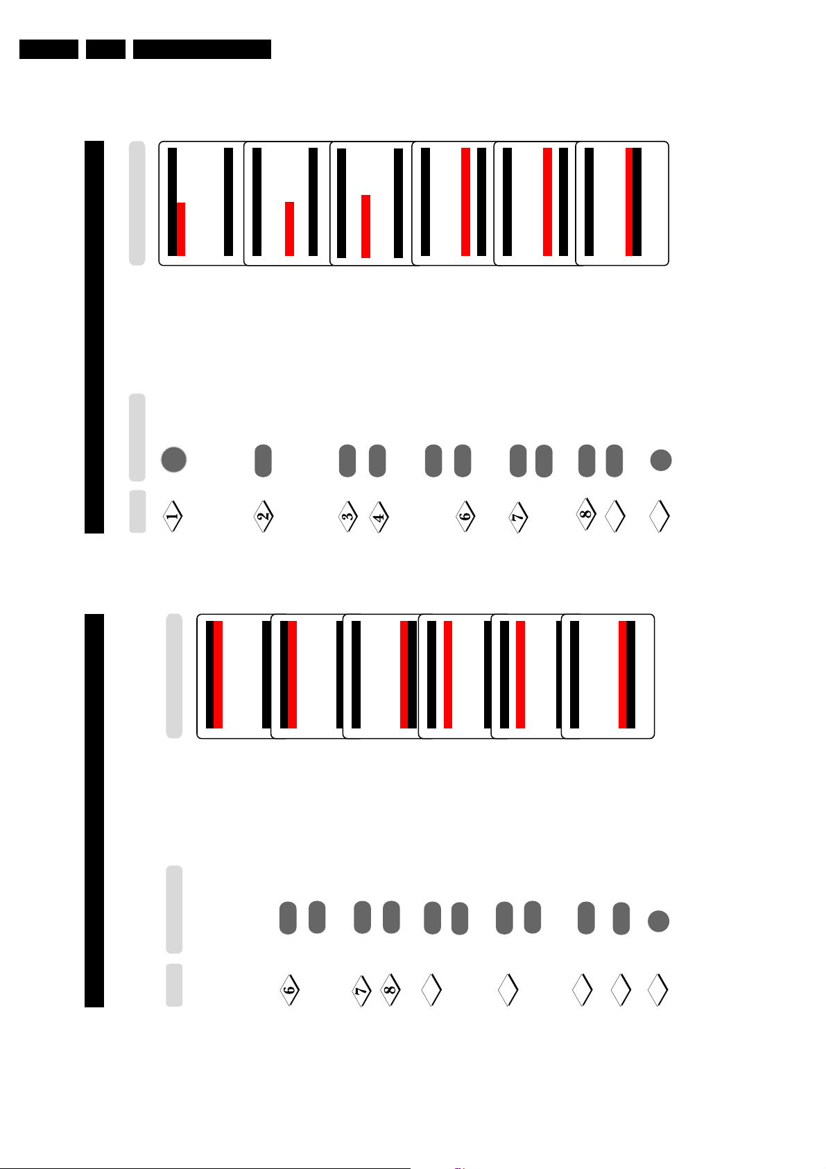
• Or via ComPair.
After entering SDM, the following screen is visible, with SDM
at the upper right side for recognition.
SW
cluster
1AP1
1AP2
1AP3
1AP9
3AP1
3AP2
4AP1
Abbreviations: A= Asia Pacific, C= NTSC, N= no TXT, T= TXT
SOFTWARE VERSIONS (L01 AP SMALL SCREEN)
SW name UOC-type Diversity
L01AN1-x.y TDA9580/1 AP, non TXT, China/AP
L01AN2-x.y TDA9581/2 AP, non TXT, Thailand/Vietnam
L01AN3-x.y TDA9580/1 AP, non TXT, India
L01AN9-x.y TDA9581 AP, non TXT, Middle East
L01AT1-x.y TDA9561/7 AP, 10 page TXT, Sgp/Aus/NZ
L01AT2-x.y TDA9567 AP, 10 page TXT, Middle East
L01AC1-x.y TDA9580 AP, NTSC, Thailand/Philippines
Figure 5-2
CL 16532008_070.pdf
220801
Page 21
Service Modes, Error Codes and Fault Finding
/STA
AAABCDEE X . Y SDM
ERRXXXXXXXXXX
MENU
SDM
Ma i n ^
• Pi cture > Brightness
• Sound Col our
• Feat ur es Contr as t
• I nst al l Sharpness
Co l ou r T emp
Store
v
GB 21L01.2A 5.
Specifications
• Operation hours counter.
• Software version.
• Option settings.
• Error buffer reading and erasing.
• Software alignments.
How to enter
Use one of the following methods:
• Use a standard customer RC-transmitter and key in the
code ‘062596’ directly followed by the OSD / STATUS
button or
• Via ComPair.
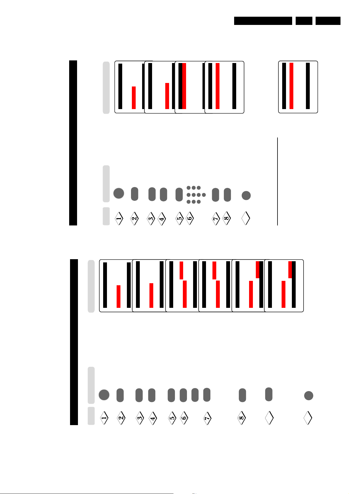
The following screen is visible, with SAM at the upper right
side for recognition.
LLLL AAABCD X . Y SAM
ERR XX XX XX XX XX
XXX XXX XXX XXX XXX XXX XXX
CLEAR CLEAR ?
OPT I ONS >
AKB 0 / 1
TUNER >
WH I T E T ON E >
GEOMETRY >
AUD I O >
CL 16532020_060.pdf
Figure 5-3
How to navigate
Use one of the following methods:
• When you press the MENU button on the remote control,
the set will switch between the SDM and the normal user
menu (with the SDM mode still active in the background).
Return to the SDM screen with the OSD / STATUS
button.
• When you press the OSD / STATUS button on the
remote control, the menu will show or hide the error
buffer. This feature is available to prevent interference
during waveform measurements.
• On the TV, press and hold the 'VOLUME down' and
press the 'CHANNEL down' for a few seconds, to switch
from SDM to SAM and reverse.
How to exit
Switch the set to STANDBY by pressing the power button on
the remote control transmitter (if you switch the set 'off' by
removing the AC power, the set will return in SDM when AC
power is re-applied). The error buffer is cleared.
5.2.2 Service Alignment Mode (SAM)
Purpose
• To perform alignments.
• To change option settings.
• To display / clear the error code buffer.
OSD
SDM
220501
TUS
CL 16532020_061.eps
150401
Figure 5-4
1. LLLL This is the operation hours counter. It counts the
normal operation hours, not the standby hours.
2. AAABCD-X.Y This is the software identification of the
main micro controller:
• A = the project name (L01).
• B = the region: E= Europe, A= Asia Pacific, U=
NAFTA, L= LATAM.
• C = the software diversity: C= NTSC, D= DVD, N= no
TXT, T= TXT.
• D = the language cluster number.
• X = the main software version number.
• Y = the sub software version number.
3. SAM Indication of the actual mode.
4. Error buffer Five errors possible.
5. Option bytes Seven codes possible.
6. Clear Erase the contents of the error buffer. Select the
CLEAR menu item and press the CURSOR RIGHT key.
The content of the error buffer is cleared.
7. Options To set the Option Bytes. See chapter 8.3.1 for
a detailed description.
8. AKB Disable (0) or enable (1) the ‘black current loop’
(AKB = Auto Kine Bias).
9. Tuner To align the Tuner. See chapter 8.3.2 for a
detailed description.
10. White Tone To align the White Tone. See chapter 8.3.3
for a detailed description.
11. Geometry To align the Geometry. See chapter 8.3.4 for
a detailed description.
12. Audio To align the Audio. See chapter 8.3.5 for a
detailed description.
How to navigate
Use one of the following methods:
• In SAM, select menu items with the CURSOR UP/DOWN
key on the remote control transmitter. The selected item
will be highlighted. When not all menu items fit on the
screen, move the CURSOR UP/DOWN key to display
the next / previous menu items.
• With the CURSOR LEFT/RIGHT keys, it is possible to:
– (De)activate the selected menu item.
– Change the value of the selected menu item.
Page 22

GB 22 L01.2A5.
Service Modes, Error Codes and Fault Finding
– Activate the selected submenu.
• When you press the MENU button twice, the set will
switch to the normal user menus (with the SAM mode still
active in the background). To return to the SAM menu
press the OSD / STATUS button [ i+ ].
• When you press the MENU key in a submenu, you will
return to the previous menu.
How to exit
Switch the set to STANDBY by pressing the power button on
the remote control (if you switch the set 'off' by removing the
AC power, the set will return in SAM when AC power is reapplied). The error buffer is not cleared.
5.2.3 Customer Service Mode (CSM)
Purpose
When a customer is having problems with his TV-set, he can
call his dealer. The service technician can than ask the
customer to activate the CSM, in order to identify the status
of the set. Now, the service technician can judge the
severness of the complaint. In a lot of cases he can advise
the customer how to solve the problem, or he can decide if it
is necessary to visit the customer.
The CSM is a read only mode, therefore modifications in this
mode are not possible.
How to enter
The CSM will be turned on after pressing the MUTE key on
the remote control transmitter and any of the control buttons
on the TV for at least 4 seconds simultaneously. This
activation only works if there is no menu on the screen.
After switching ON the Customer Service Mode, the following
screen will appear:
10. Value indicates parameter levels at CSM entry (only for
stereo sets). TR= TREBLE, BS= BASS
How to exit
Use one of the following methods:
• After you press ‘any’ key of the remote control transmitter
with exception of the CHANNEL and VOLUME keys.
• After you switch-off the TV set with the AC power switch.
5.3 Problems and Solving Tips (Related to CSM)
5.3.1 Picture Problems
Note: Below described problems are all related to the TV
settings. The procedures to change the value (or status) of
the different settings are described.
No colours / noise in picture
Check CSM line 4. Wrong colour system installed. To change
the setting:
1. Press the MENU button on the remote control.
2. Select the INSTALL sub menu.
3. Select the MANUAL STORE sub menu.
4. Select and change the SYSTEM setting until picture and
sound are correct.
5. Select the STORE menu item.
Colours not correct / unstable picture
Check CSM line 4. Wrong colour system installed. To change
the setting:
1. Press the MENU button on the remote control.
2. Select the INSTALL sub menu.
3. Select the MANUAL STORE sub menu.
4. Select and change the SYSTEM setting until picture and
sound are correct.
5. Select the STORE menu item.
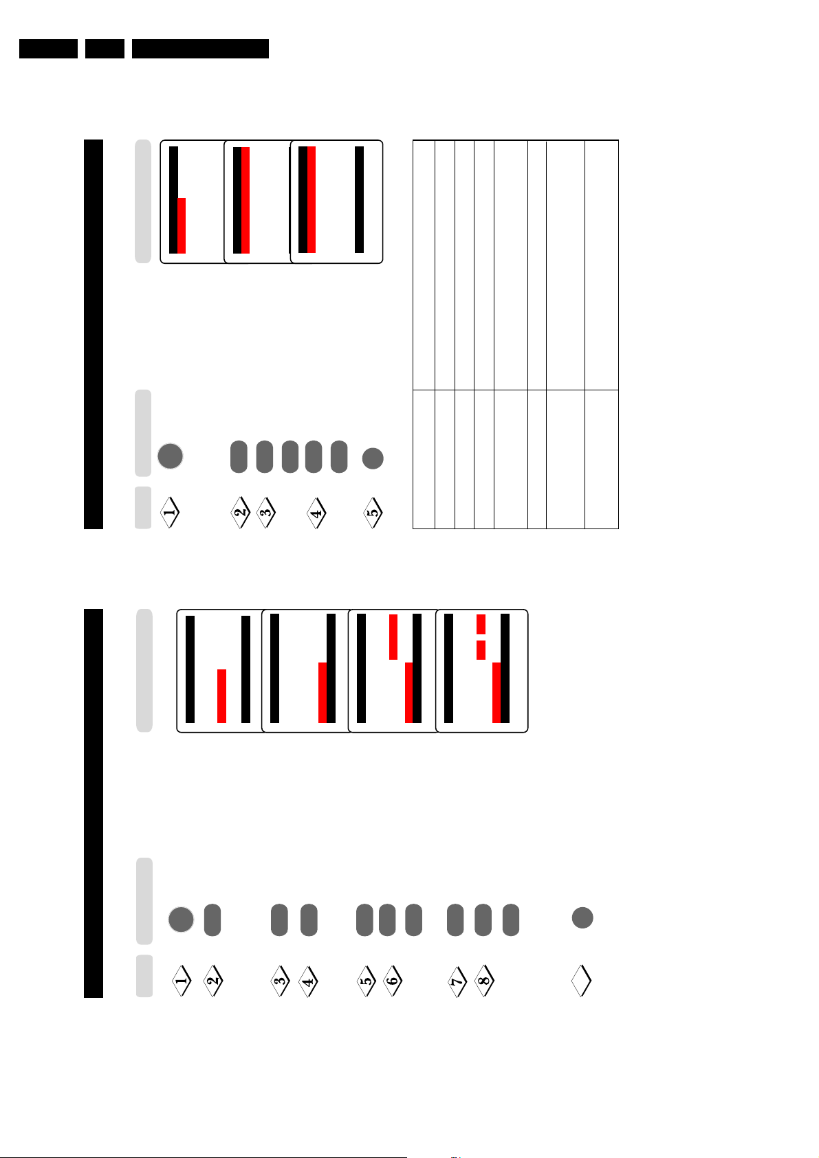
1AAABCD X.Y CSM
2 CODES XX XX XX XX XX
3 OP XXX XXX XXX XXX XXX XXX XXX
4 DETECTED SYSTEM DETECTED SOUND
5 NOT TUNED SKIPPED
6TIMER
7
8 CO XX C L XX BR XX HU XX SH XX
9VLXX BL XX AVL DVXX
10 TR XX BS XX
CL 16532008_046.eps
220501
Figure 5-5
1. Software identification of the main micro controller (see
paragraph 5.2.2 for an explanation).
2. Error code buffer (see paragraph 5.5 for more details).
Displays the last seven errors of the error code buffer.
3. In this line, the Option Bytes (OB) are visible. Each
Option Byte is displayed as a decimal number between 0
and 255. The set may not work correctly when an
incorrect option code is set. See chapter 8.3.1 for more
information on the option settings.
4. Indicates which color and sound system is installed for
the selected pre-set.
5. Indicates if the set is not receiving an ‘IDENT’ signal on
the selected source. It will display ‘Not Tuned’.
6. Indicates if the sleep timer is enabled.
7. Indicates if the V-chip feature is enabled.
8. Value indicates parameter levels at CSM entry. CO=
CONTRAST, CL= COLOR, BR= BRIGHTNESS, HU=
HUE, SH= SHARPNESS
9. Value indicates parameter levels at CSM entry. VL=
VOLUME LEVEL, BL= BALANCE LEVEL, AVL= AUTO
VOLUME LEVEL LIMITER, DV= DELTA VOLUME
TV switches ‘off’ (or ‘on’) or changes the channel without
any user action
(Sleep)timer switched the set ‘off’ or changed channel. To
change the setting:
1. Press the MENU button on the remote control.
2. Select the FEATURES sub menu.
3. Select the TIMER sub menu.
4. Select and change the SLEEP or TIME setting.
Picture too dark or too bright
Increase / decrease the BRIGHTNESS and / or the
CONTRAST value when:
• The picture improves after you have pressed the ‘Smart
Picture’ button on the remote control.
• The picture improves after you have switched on the
Customer Service Mode
The new ‘Personal’ preference value is automatically stored.
White line around picture elements and text
Decrease the SHARPNESS value when:
• The picture improves after you have pressed the ‘Smart
Picture’ button on the remote control.
• The picture improves after you have switched on the
Customer Service Mode
The new ‘Personal’ preference value is automatically stored.
Snowy picture
Check CSM line 5. If this line indicates ‘Not Tuned’, check the
following:
• No or bad antenna signal. Connect a proper antenna
signal.
• Antenna not connected. Connect the antenna.
• No channel / pre-set is stored at this program number.
Go to the INSTALL menu and store a proper channel at
this program number.
Page 23

Service Modes, Error Codes and Fault Finding
GB 23L01.2A 5.
• The tuner is faulty (in this case the CODES line will
contain error number 10). Check the tuner and replace /
repair if necessary.
Snowy picture and/or unstable picture
• A scrambled or decoded signal is received.
Black and white picture
Increase the COLOR value when:
• The picture improves after you have pressed the ‘Smart
Picture’ button on the remote control.
• The picture improves after you have switched on the
Customer Service Mode
The new ‘Personal’ preference value is automatically stored.
Menu text not sharp enough
Decrease the CONTRAST value when:
• The picture improves after you have pressed the ‘Smart
Picture’ button on the remote control.
• The picture improves after you have switched on the
Customer Service Mode
The new ‘Personal’ preference value is automatically stored.
5.3.2 Sound Problems
No sound or sound too loud (after channel change /
switching on)
Increase / decrease the VOLUME level when the volume is
OK after you switched on the CSM. The new ‘Personal’
preference value is automatically stored.
5.4 ComPair
5.4.1 Introduction
ComPair can access the I
ComPair can send and receive I
2
C bus of the television.
2
C commands to the
micro controller of the television. In this way, it is possible
for ComPair to communicate (read and write) to devices
2
C busses of the TV-set.
on the I
• Manually (by asking questions to you): Automatic
diagnosis is only possible if the micro controller of the
television is working correctly and only to a certain
extend. When this is not the case, ComPair will guide you
through the faultfinding tree by asking you questions
(e.g. Does the screen gives a picture? Click on the
correct answer: YES / NO) and showing you examples
(e.g. Measure test-point I7 and click on the correct
oscillogram you see on the oscilloscope). You can
answer by clicking on a link (e.g. text or a waveform
picture) that will bring you to the next step in the
faultfinding process.
By a combination of automatic diagnostics and an interactive
question / answer procedure, ComPair will enable you to find
most problems in a fast and effective way.
Beside fault finding, ComPair provides some additional
features like:
• Up- or downloading of pre-sets.
• Managing of pre-set lists.
• Emulation of the (European) Dealer Service Tool (DST).
• If both ComPair and SearchMan (Electronic Service
Manual) are installed, all the schematics and the PWBs
of the set are available by clicking on the appropriate
hyperlink. Example: Measure the DC-voltage on
capacitor C2568 (Schematic/Panel) at the
Monocarrier.Click on the ‘Panel’ hyperlink to
automatically show the PWB with a highlighted capacitor
C2568. Click on the ‘Schematic’ hyperlink to
automatically show the position of the highlighted
capacitor.
ComPair (Computer Aided Repair) is a service tool for Philips
Consumer Electronics products. ComPair is a further
development on the European DST (service remote control),
which allows faster and more accurate diagnostics. ComPair
has three big advantages:
• ComPair helps you to quickly get an understanding on
how to repair the chassis in a short time by guiding you
systematically through the repair procedures.
• ComPair allows very detailed diagnostics (on I
and is therefore capable of accurately indicating problem
areas. You do not have to know anything about I
commands yourself because ComPair takes care of this.
• ComPair speeds up the repair time since it can
automatically communicate with the chassis (when the
microprocessor is working) and all repair information is
directly available. When ComPair is installed together
with the SearchMan electronic manual of the defective
chassis, schematics and PWBs are only a mouse click
away.
5.4.2 Specifications
ComPair consists of a Windows based faultfinding program
and an interface box between PC and the (defective)
product. The ComPair interface box is connected to the PC
via a serial or RS232 cable.
In case of the L01 chassis, the ComPair interface box and the
TV communicate via a bi-directional service cable via the
service connector (located on the Main panel, see also figure
8-1 suffix D).
The ComPair faultfinding program is able to determine the
problem of the defective television. ComPair can gather
diagnostic information in two ways:
• Automatic (by communication with the television):
ComPair can automatically read out the contents of the
entire error buffer. Diagnosis is done on I
2
C level.
2
C level)
2
C
5.4.3 How to Connect
1. First install the ComPair Browser software (see the Quick
Reference Card for installation instructions).
2. Connect the RS232 interface cable between a free serial
(COM) port of your PC and the PC connector (marked
with ‘PC’) of the ComPair interface.
3. Connect the AC power adapter to the supply connector
(marked with ‘POWER 9V DC’) on the ComPair
interface.
4. Switch the ComPair interface OFF.
5. Switch the television set OFF (remove the AC power).
6. Connect the ComPair interface cable between the
connector on the rear side of the ComPair interface
(marked with ‘I
2
C’) and the ComPair connector on the
mono carrier (see figure 8-1 suffix D).
7. Plug the AC power adapter in the AC power outlet and
switch on the interface. The green and red LEDs light up
together. The red LED extinguishes after approx. 1
second while the green LED remains lit.
8. Start the ComPair program and read the ‘introduction’
chapter.
PC VCR I2CPower
Figure 5-6
9V DC
86532027_003.EPS
050898
Page 24

GB 24 L01.2A5.
Service Modes, Error Codes and Fault Finding
5.4.4 How to Order
ComPair order codes:
• Starter kit ComPair + SearchMan software + ComPair
interface (excluding transformer): 4822 727 21629
• ComPair interface (excluding transformer): 4822 727
21631
• Starter kit ComPair software (registration version): 4822
727 21634
• Starter kit SearchMan software: 4822 727 21635
• ComPair CD (update): 4822 727 21637
• SearchMan CD (update): 4822 727 21638
• ComPair interface cable: 3122 785 90004
5.5 Error Buffer
The error code buffer contains all detected errors since the
last time the buffer was erased. The buffer is written from left
to right. When an error occurs that is not yet in the error code
buffer, it is written at the left side and all other errors shift one
position to the right.
5.5.1 How to Read the Error Buffer
Use one of the following methods:
• On screen via the SAM (only if you have a picture).
Examples:
– ERROR: 0 0 0 0 0 : No errors detected
– ERROR: 6 0 0 0 0 : Error code 6 is the last and only
detected error
– ERROR: 9 6 0 0 0 : Error code 6 was first detected
and error code 9 is the last detected (newest) error
• Via the blinking LED procedure (when you have no
picture). See next paragraph.
• Via ComPair.
5.5.2 How to Clear the Error Buffer
The error code buffer is cleared in the following cases:
• By activation of the CLEAR command in the SAM menu:
• When you exit SDM / SAM with the STANDBY command
on the remote control (when leaving SDM / SAM, by
disconnecting the set from AC power, the error buffer is
not reset).
• When you transmit the command DIAGNOSE-99-OK
with ComPair.
• If the content of the error buffer has not changed for 50
hours, it resets automatically.
5.5.3 Error Codes
In case of non-intermittent faults, clear the error buffer before
you begin the repair. These to ensure that old error codes are
no longer present.
If possible, check the entire contents of the error buffer. In
some situations, an error code is only the result of another
error code and not the actual cause (e.g., a fault in the
protection detection circuitry can also lead to a protection).
CL 16532008_047.pdf
Figure 5-7
210501
Page 25

Service Modes, Error Codes and Fault Finding
GB 25L01.2A 5.
5.6 The Blinking LED Procedure
Via this procedure, you can make the contents of the error
buffer visible via the front LED. This is especially useful when
there is no picture.
When the SDM is entered, the LED will blink the contents of
the error-buffer.
Error-codes ³ 10 are shown as follows:
– a long blink of 750 ms (which is an indication of the
decimal digit),
– a pause of 1.5 s,
– n short blinks (n = 1 - 9),
– when all the error-codes are displayed, the sequence
finishes with a LED blink of 3 s,
– the sequence starts again.
Example of error buffer: 12 9 6 0 0
After entering SDM:
– 1 long blink of 750 ms followed by a pause of 1.5 s,
– 2 short blinks followed by a pause of 3 s,
– 9 short blinks followed by a pause of 3 s,
– 6 short blinks followed by a pause of 3 s,
– 1 long blink of 3 s to finish the sequence,
– the sequence starts again.
5.7 Protections
the same time, measure the ‘+8V’. If this voltage is
missing, check transistor TS7480.
• Set is non-stop in hiccup mode Set is in over current
mode; check the secondary sensing (opto coupler 7515)
and the ‘MainSupply’ voltage. Signal ‘Stdby_con’ must
be logic low under normal operation conditions and goes
to high (3.3 V) under standby and fault conditions.
• Set turns on, but without picture and sound The
screen shows snow, but OSD and other menus are okay.
Blinking LED procedure indicates error 11, so problem is
expected in the tuner (pos. 1000). Check presence of
supply voltages. As ‘Vlotaux+5V’ at pin 5 and 7 are okay,
‘VT_supply’ at pin 9 is missing. Conclusion: resistor 3460
is defective.
• Set turns on, but with a half screen at the bottom.
Sound is okay Blinking LED (set in SDM mode)
indicates error 3. Check ‘Vlotaux+13V’ and ‘+50V’. If they
are okay, problem is expected in the vertical amplifier
IC7471. Measure with a scope the waveform on pin 17 of
the UOC. Measure also at pin 1 of IC7471. If here the
signal is missing, a defective resistor R3244 causes the
problem.
If a fault situation is detected an error code will be generated
and if necessary, the set will be put in the protection mode.
Blinking of the red LED at a frequency of 3 Hz indicates the
protection mode. In some error cases, the microprocessor
does not put the set in the protection mode. The error codes
of the error buffer can be read via the service menu (SAM),
the blinking LED procedure or via ComPair. The DST
diagnose functionality will force the set into the Servicestandby, which is similar to the usual standby mode, however
the microprocessor has to remain in normal operation
completely.
To get a quick diagnosis the chassis has three service modes
implemented:
• The Customer Service Mode (CSM).
• The Service Default Mode (SDM). Start-up of the set in a
predefined way.
• The Service Alignment Mode (SAM). Adjustment of the
set via a menu and with the help of test patterns.
See for a detailed description Chapter 9 paragraphs
Deflection and Power Supply.
5.8 Repair Tips
Below some failure symptoms are given, followed by a repair
tip.
• Set is dead and makes hiccuping sound ‘MainSupply’
is available. Hiccuping stops when de-soldering L5561,
meaning that problem is in the ‘MainSupply’ line. No
output voltages at LOT, no horizontal deflection. Reason:
line transistor TS7460 is defective.
• Set is dead, and makes no sound Check power supply
IC7520. Result: voltage at pins 1, 3, 4, 5 and 6 are about
180 V and pin 8 is 0 V. The reason why the voltage on
these pins is so high is because the output driver (pin 6)
has an open load. That is why MOSFET TS7521 is not
able to switch. Reason: feedback resistor 3523 is
defective. Caution: be careful measuring on the gate of
TS7521; circuitry is very high ohmic and can easily be
damaged! (first connect measuring equipment to ground,
then to the gate).
• Set is in hiccup mode and shuts down after 8 s.
Blinking LED (set in SDM mode) indicates error 5. As it
is unlikely that mP ‘POR’ and ‘+8V protection’ happen at
Page 26

GB 26 L01.2A5.
Personal Notes:
Service Modes, Error Codes and Fault Finding
Page 27

8. Alignments
Alignments
GB 53L01.2A 8.
Index:
1. General Alignment Conditions
2. Hardware Alignments
3. Software Alignments and Settings
Note:
• The Service Default Mode (SDM) and Service Alignment
Mode (SAM) are described in chapter 5.
• Menu navigation is done with the 'CURSOR UP, DOWN,
LEFT or RIGHT' keys of the remote control transmitter.
• Figures can deviate slightly from the actual situation, due
to different set executions or software versions.
8.1 General Alignment Conditions
Perform all electrical adjustments under the following
conditions:
• AC voltage and frequency: according to country’s
standard.
• Connect the set to the AC power via an isolation
transformer.
• Allow the set to warm up for approximately 20 minutes.
• Measure the voltages and waveforms in relation to
chassis ground (with the exception of the voltages on the
primary side of the power supply). Never use the cooling
fins / plates as ground.
• Test probe: Ri > 10 MW; Ci < 2.5 pF.
• Use an isolated trimmer / screwdriver to perform the
alignments.
3. Set the values of NORMAL RED, GREEN and BLUE to
40.
4. Go, via the MENU key, to the normal user menu and set
– CONTRAST to zero.
– BRIGHTNESS to minimum (OSD just visible in a
dark room).
5. Return to the SAM via the MENU key.
6. Connect the RF output of a pattern generator to the
antenna input. Test pattern is a 'black' picture (blank
screen on CRT without any OSD info).
7. Set the channel of the oscilloscope to 50 V/div and the
time base to 0.2 ms (external triggering on the vertical
pulse).
8. Ground the scope at the CRT panel and connect a 10:1
probe to one of the cathodes of the picture tube socket
(see diagram B).
9. Measure the cut off pulse during first full line after the
frame blanking (see Fig. 8-2). You will see two pulses,
one being the cut off pulse and the other being the white
drive pulse. Choose the one with the lowest value, this is
the cut off pulse.
10. Select the cathode with the highest V
alignment. Adjust the V
of this gun with the SCREEN
cutoff
value for the
DC
potentiometer (see Fig. 8-1) on the LOT to the correct
value (see table below).
11. Restore BRIGHTNESS and CONTRAST to normal (=
31).
8.2 Hardware Alignments
0217
D
ComPair
1004
1002
1000 (TUNER)
2403
9631
7602
A
9641
SDM
Figure 8-1
max.
V
CUTOFF
[VDC]
0V Ref.
0231
C
0212
0231
CL 06532130_014.eps
131000
Figure 8-2
CUT-OFF VOLTAGE
0" 140 ± 4
150 ± 4
125 ± 4
145 ± 10
CL 16532008_058.pdf
220801
5520
Screen size Cut-off [V]
13V, 14", 14RF, 15RF, 17", 19V, 2
21" (L01S)
21" (L01L), 20RF, 21RF, 24WS,
25BLD, 25HF, 28 BLD, 28WS
25V, 25BLS, 25RF, 27V, 28BLS, 29",
29RF, 32V, 33", 32WS, 35V
Figure 8-3
B
Focus
Screen
5445
LOT
VG2
8.2.2 Focusing
1. Tune the set to a circle or crosshatch test pattern (use an
external video pattern generator).
2. Choose picture mode NATURAL (or MOVIES) with the
‘SMART PICTURE’ button on the remote control
16532016_003.eps
120401
transmitter.
3. Adjust the FOCUS potentiometer (see Fig. 8-1) until the
vertical lines at 2/3 from east and west, at the height of
the centreline, are of minimum width without visible haze.
8.2.1 Vg2 Adjustment
1. Activate the SAM.
2. Go to the WHITE TONE sub menu.
8.3 Software Alignments and Settings
Enter the Service Alignment Mode (see chapter 5). The SAM
menu will now appear on the screen.
Page 28

GB 54 L01.2A8.
Alignments
Select one of the following alignments:
1. OPTIONS
2. TUNER
3. WHITE TONE
4. GEOMETRY
5. AUDIO
8.3.1 Options
SAM
OP1 XXX
OP2 XXX
OP3 XXX
OP4 XXX
OP5 XXX
OP6 XXX
OP7 XXX
CL 16532008_048.pdf
Figure 8-4
Options are used to control the presence / absence of certain
features and hardware.
How to change an Option Byte
An Option Byte represents a number of different options.
Changing these bytes directly makes it possible to set all
options very fast. All options are controlled via seven option
bytes. Select the option byte (OB1.. OB7) with the MENU UP/
DOWN keys, and enter the new value.
Leaving the OPTION submenu saves changes in the Option
Byte settings. Some changes will only take effect after the set
has been switched OFF and ON with the AC power switch
(cold start).
How to calculate the value of an Option Byte
Calculate an Option Byte value (OB1 .. OB7) in the following
way:
1. Check the status of the single option bits (OP): are they
enabled (1) or disabled (0).
2. When an option bit is enabled (1) it represents a certain
value (see first column ‘value between brackets’ in first
table below). When an option bit is disabled, its value is
0.
3. The total value of an Option Byte is formed by the sum of
its eight option bits. See second table below for the
correct Option Bytes per typenumber.
CL 16532008_049.pdf
220501
210501
Typenumber OB1 OB2 OB3 OB4 OB5 OB6 OB7
14PT2001/59A
14PT2001/59B
14PT2001/59C
14PT2001/65R
14PT2001/67R
14PT2001/71R
14PT2001/79R
14PT2011/71R
14PT2011/74R
14PT2012/59A
14PT2012/59B
14PT2012/59C
14PT2012/65R
14PT2401/94R
14PT2411/94R
15PT2301/67R
15PT2301/71R
15PT2301/74R
15PT2302/56A
15PT2302/57R
15PT2302/65R
15PT2302/68R
15PT2302/69R
15PT2302/79R
15PT2441/94R
20PT2001/59A
20PT2001/59B
20PT2001/59C
20PT2001/59S
20PT2001/65R
20PT2001/67R
20PT2001/71R
20PT2001/79R
20PT2011/67R
20PT2011/71R
20PT2011/74R
20PT2012/59A
20PT2012/59B
20PT2012/59C
20PT2012/59S
20PT2012/65R
20PT2151/67R
20PT2151/71R
20PT2151/74R
20PT2152/65R
20PT2152/68R
20PT2152/69R
20PT2401/94R
20PT2411/94R
20PT2421/94R
21PT2001/59B
21PT2001/67R
21PT2001/71R
21PT2001/79R
21PT2011/67R
21PT2011/71R
21PT2011/74R
21PT2012/59A
21PT2012/59B
21PT2012/59C
21PT2012/65R
21PT2012/79R
21PT2411/94R
21PT2421/94R
21PT2425/94R
21PT2426/94R
21PT2501/93R
21PT2502/93R
21PT2521/93R
0 215 65 0 194 80 9
0 215 65 0 194 80 9
0 215 65 0 194 80 9
0 215 65 0 194 80 9
0 215 65 0 194 80 9
0 215 65 0 194 80 4
0 215 65 0 194 80 11
0 215 65 0 210 80 4
0 215 65 0 210 80 9
0 247 65 0 210 80 9
0 247 65 0 210 80 9
0 247 65 0 210 80 9
0 247 65 0 210 80 9
192 215 65 0 194 80 0
192 215 65 0 194 80 0
160 215 65 168 246 144 44
160 215 65 162 246 144 36
160 215 65 168 246 144 44
160 247 65 168 246 144 44
160 247 65 168 246 144 44
160 247 65 168 246 144 44
160 247 65 168 246 144 44
160 247 65 168 246 144 44
160 247 65 168 246 144 44
192 215 65 164 246 144 12
0 215 65 0 194 80 9
0 215 65 0 194 80 9
0 215 65 0 194 80 9
0 215 65 0 194 80 9
0 215 65 0 194 80 9
0 215 65 0 194 80 9
0 215 65 0 194 80 4
0 215 65 0 194 80 11
160 215 65 0 210 80 41
160 215 65 0 210 80 36
160 215 65 0 210 80 41
160 247 65 0 210 80 41
160 247 65 0 210 80 41
160 247 65 0 210 80 41
160 247 65 0 210 80 41
160 247 65 0 210 80 41
160 215 65 164 242 80 44
160 215 65 162 242 80 36
160 215 65 164 242 80 44
160 247 65 164 242 80 44
160 247 65 164 242 80 44
160 247 65 164 242 80 44
0 215 65 0 194 80 0
192 215 65 0 194 80 0
160 215 65 164 210 80 32
0 215 65 0 194 80 9
0 215 65 0 194 80 9
0 215 65 0 194 80 4
0 215 65 0 194 80 11
160 215 65 0 194 80 41
160 215 65 0 194 80 36
160 215 65 0 194 80 41
0 247 65 0 194 80 9
160 247 65 0 194 80 41
0 247 65 0 194 80 9
160 247 65 0 194 80 41
160 247 65 0 194 80 43
0 215 65 0 210 80 0
192 215 65 164 226 80 0
192 215 65 164 242 144 0
192 215 65 164 242 144 0
1 215 65 0 194 16 3
1 215 65 0 194 16 3
1 215 65 164 226 16 3
CL 16532008_071.pdf
220801
Figure 8-5
Figure 8-6
Page 29

Alignments
GB 55L01.2A 8.
Option Bit Assignment
Following are the option bit assignments for all L01 software
clusters.
• Option Byte 1 (OB1)
– OP10: CHINA
– OP11: VIRGIN_MODE
– OP12: UK_PNP
– OP13: ACI
– OP14: ATS
– OP15: LNA
– OP16: FM_RADIO
– OP17: PHILIPS_TUNER
• Option Byte 2 (OB2)
– OP20: HUE
– OP21: COLOR_TEMP
– OP22: CONTRAST_PLUS
– OP23: TILT
– OP24: NOISE_REDUCTION
– OP25: CHANNEL_NAMING
– OP26: SMART_PICTURE
– OP27: SMART_SOUND
• Option Byte 3 (OB3)
– OP30: AVL
– OP31: WSSB
– OP32: WIDE_SCREEN
– OP33: SHIFT_HEADER_SUBTITLE
– OP34: CONTINUOUS_ZOOM
– OP35: COMPRESS_16_9
– OP36: EXPAND_4_3
– OP37: EW_FUNCTION
• Option Byte 4 (OB4)
– OP40: STEREO_NON_DBX
– OP41: STEREO_DBX
– OP42: STEREO_PB
– OP43: STEREO_NICAM_2CS
– OP44: DELTA_VOLUME
– OP45: ULTRA_BASS
– OP46: VOLUME_LIMITER
– OP47: INCR_SUR
• Option Byte 5 (OB5)
– OP50: PIP
– OP51: HOTEL_MODE
– OP52: SVHS
– OP53: CVI
– OP54: AV3
– OP55: AV2
– OP56: AV1
– OP57: NTSC_PLAYBACK
• Option Byte 6 (OB6)
– OP60: Reserved (value = 0)
– OP61: SMART_TEXT
– OP62: SMART_LOCK
– OP63: VCHIP
– OP64: WAKEUP_CLOCK
– OP65: SMART_CLOCK
– OP66: SMART_SURF
– OP67: PERSONAL_ZAPPING
• Option Byte 7 (OB7)
– OP70: SOUND_SYSTEM_AP_3 /
MULTI_STANDARD_EUR / SYSTEM_LT_2
– OP71: SOUND_SYSTEM_AP_2 / WEST_EU
/ SYSTEM_LT_1
– OP72: SOUND_SYSTEM_AP_1
– OP73: COLOR_SYSTEM_AP
– OP74: Reserved (value = 0)
– OP75: Reserved (value = 0)
– OP76: TIME_WIN2
– OP77: TIME_WIN1
Option bit definition
• OP10: CHINA0 : Tuning is not for China set, or this
option bit is not applicable, 1 : Tuning is for China set,
Default setting : 0.
• OP11: VIRGIN_MODE0 : Virgin mode is disabled or not
applicable, 1 : Virgin mode is enabled. Plug and Play
menu item will be displayed to perform installation at the
initial start-up of the TV when VIRGIN_MODE is set to 1.
After installation is finished, this option bit will be
automatically set to 0, Default setting : 0.
• OP12: UK_PNP0 : UK's default Plug and Play setting is
not available or not applicable, 1 : UK's default Plug and
Play setting is available. When UK_PNP and
VIRGIN_MODE are set to 1 at the initial set-up,
LANGUAGE = ENGLISH, COUNTRY = GREAT
BRITAIN and after exiting from menu, VIRGIN_MODE
will be set automatically to 0 while UK_PNP remains 1,
Default setting : 0.
• OP13: ACI0 : ACI feature is disabled or not applicable, 1
: ACI feature is enabled, Default setting : 0.
• OP14: ATS0 : ATS feature is disabled or not applicable,
1 : ATS feature is enabled. When ATS is enabled, it sorts
the program in an ascending order starting from program
1, Default setting : 0.
• OP15: LNA0 : Auto Picture Booster is not available or not
applicable, 1 : Auto Picture Booster is available, Default
setting : 0.
• OP16: FM_RADIO0 : FM radio feature is disabled or not
applicable, 1 : FM radio feature is enabled, Default
setting : 0.
• OP17: PHILIPS_TUNER0 : ALPS / MASCO compatible
tuner is in use, 1 : Philips compatible tuner is in use,
Default setting : 0.
• OP20: HUE0 : Hue/Tint Level is disabled or not
applicable, 1 : Hue/Tint Level is enabled, Default setting
: 0.
• OP21: COLOR_TEMP0 : Colour Temperature is
disabled or not applicable, 1 : Colour Temperature is
enabled, Default setting : 0.
• OP22: CONTRAST_PLUS0 : Contrast+ is disabled or
not applicable, 1 : Contrast+ is enabled, Default setting :
0.
• OP23: TILT0 : Rotate Picture is disabled or not
applicable, 1 : Rotate Picture is enabled, Default setting
: 0.
• OP24: NOISE_REDUCTION0 : Noise Reduction (NR) is
disabled or not applicable, 1 : Noise Reduction (NR) is
enabled, Default setting : 0.
• OP25: CHANNEL_NAMING0 : Name FM Channel is
disabled or not applicable, 1 : Name FM Channel is
enabled, Default setting : 0. Note : Name FM channel can
be enabled only when FM_RADIO = 1.
• OP26: SMART_PICTURE0 : Smart Picture is disabled or
not applicable, 1 : Smart Picture is enabled, Default
setting : 1
• OP27: SMART_SOUND0 : Smart Sound is disabled or
not applicable, 1 : Smart Sound is enabled, Default
setting : 1
• AP30: AVL0 : AVL is disabled or not applicable, 1 : AVL
is enabled, Default setting : 0.
• OP31: WSSB0 : WSSB is disabled or not applicable, 1 :
WSSB is enabled, Default setting : 0. Note : This option
bit can be set to 1 only when WIDE_SCREEN = 1.
• OP32: WIDE_SCREEN0 : Software is used for 4:3 set or
not applicable, 1 : Software is used for 16:9 set, Default
setting : 0.
• OP33: SHIFT_HEADER_SUBTITLE0 : Shift Header /
Subtitle is disabled or not applicable, 1 : Shift Header /
Subtitle is enabled, Default setting : 0. Note : This option
bit can be set to 1 only when WIDE_SCREEN = 1.
• OP34: CONTINUOUS_ZOOM0 : Continuous Zoom is
disabled or not applicable, 1 : Continuous Zoom is
enabled, Default setting : 0. Note : This option bit can be
set to 1 only when WIDE_SCREEN = 1.
• OP35: COMPRESS_16_90 : COMPRESS 16:9
selection is not applicable. Item should not be in the
FORMAT menu list, 1 : COMPRESS 16:9 selection is
applicable. Item should not be in the FORMAT menu list,
Default setting : 0.
• OP36: EXPAND_4_30 : Expand 4:3 selection is not
applicable. Item should not be in the FORMAT menu list,
Page 30

GB 56 L01.2A8.
A
M
Alignments
1 : Expand 4:3 selection is applicable. Item should be in
the FORMAT menu list, Default setting : 0.
• OP37: EW_FUNCTION0 : EW function is disabled. In
this case, only Expand 4:3 is allowed, Compress 16:9 is
not applicable. 1 : EW function is enabled. In this case,
both Expand 4:3 and Compress 16:9 are applicable.
Default setting : 0.
• OP40: STEREO_NON_DBX0 : For AP_NTSC, chip TDA
9853 is not present, 1 : For AP_NTSC, chip TDA 9853 is
present, Default setting : 0.
• OP41: STEREO_DBX0 : For AP_NTSC, chip MSP 3445
is not present, 1 : For AP_NTSC, chip MSP 3445 is
present, Default setting : 0.
• OP42: STEREO_PB0 : For AP_PAL, chip MSP3465 is
not present, 1 : For AP_PAL, chip MSP3465 is present,
Default setting : 0.
• OP43: STEREO_NICAM_2CS0 : For EU and AP_PAL,
chip MSP 3415 is not present, 1 : For EU and AP_PAL,
chip MSP 3415 is present, Default setting : 0.
• OP44: DELTA_VOLUME0 : Delta Volume Level is
disabled or not applicable, 1 : Delta Volume Level is
enabled, Default setting : 0.
• OP45: ULTRA_BASS0 : Ultra Bass is disabled or not
applicable, 1 : Ultra Bass is enabled, Default setting : 0.
• OP46: VOLUME_LIMITER0 : Volume Limiter Level is
disabled or not applicable, 1 : Volume Limiter Level is
enabled, Default setting : 0.
• OP47: INCR_SUR0 : Incredible Surround feature is
disabled, 1 : Incredible Surround feature is enabled,
Default setting : 1
• OP50: PIP0 : PIP is disabled or not applicable, 1 : PIP is
enabled, Default setting : 0.
• OP51: HOTEL_MODE0 : Hotel mode is disabled or not
applicable, 1 : Hotel mode is enabled, Default setting : 0.
• OP52: SVHS0 : SVHS source is not available, 1 : SVHS
source is available, Default setting : 0. Note : This option
bit is not applicable for EU.
• OP53: CVI0 : CVI source is not available, 1 : CVI source
is available, Default setting : 0.
• OP54: AV30 : Side/Front AV3 source is not present, 1 :
Side/Front AV3 source is present, Default setting : 0.
• OP55: AV20 : AV2 source is not present, 1 : AV2 source
is present, Default setting : 0. Note : For EU, when
AV2=1, both EXT2 and SVHS2 should be included in the
OSD loop.
• OP56: AV10 : AV1 source is not present, 1 : AV1 source
is present, Default setting : 0.
• OP57: NTSC_PLAYBACK0 : NTSC playback feature is
not available, 1 : NTSC playback feature is available,
Default setting : 0.
• OP60: Reserved Default setting : 0.
• OP61: SMART_TEXT0 : Smart Text Mode and Favourite
Page are disabled or not applicable, 1 : Smart Text Mode
and Favourite Page are enabled, Default setting : 1.
• OP62: SMART_LOCK 0 : Child Lock and Lock Channel
are disabled or not applicable for EU, 1 : Child Lock and
Lock Channel are enabled for EU, Default setting : 1.
• OP63: VCHIP0 : VCHIP feature is disabled, 1 : VCHIP
feature is enabled, Default setting : 1.
• OP64: WAKEUP_CLOCK0 : Wake up clock feature is
disabled or not applicable, 1 : Wake up clock feature is
enabled, Default setting : 1.
• OP65: SMART_CLOCK0 : Smart Clock Using Teletext
and Smart Clock Using PBS is disabled or not applicable,
1 : Smart Clock Using Teletext and Smart Clock Using
PBS is enabled. For NAFTA, menu item AUTOCHRON
is present in the INSTALL submenu, Default setting : 0.
• OP66: SMART_SURF0 : Smart Surf feature is disabled
or not applicable, 1 : Smart Surf feature is enabled,
Default setting : 0.
• OP67: PERSONAL_ZAPPING0 : Personal Zapping
feature is disabled or not applicable, 1 : Personal
Zapping feature is enabled, Default setting : 0.
• OP70: MULTI_STANDARD_EUR0 : Not for Europe
multi standard set, or this option bit is not applicable, 1 :
For Europe multi standard set. Default setting : 0. Note :
This option bit is used to control the SYSTEM selection
in Manual Store : If MULTI_STANDARD_EUR = 1 then
SYSTEM = Europe, West Europe, East Europe, UK,
France otherwise SYSTEM = ‘Europe, West Europe, UK
for West Europe’ (WEST_EU=1) or SYSTEM = ‘Europe,
West Europe, East Europe for East Europe’
(WEST_EU=0)
• OP71: WEST_EU0 : For East Europe set, or this option
bit is not applicable, 1 : For West Europe set, Default
setting : 0.
• OP71 and 70: SYSTEM_LT_1, SYSTEM_LT_2These
two option bits are allocated for LATAM system
selection. 00 : NTSC-M 01 : NTSC-M, PAL-M 10 :
NTSC-M, PAL-M, PAL-N 11 : NTSC-M, PAL-M, PAL-N,
PAL-BG Default setting : 00
• OP70, 71 and 72: SOUND_SYSTEM_AP_1,
SOUND_SYSTEM_AP_2,
SOUND_SYSTEM_AP_3These three option bits are
allocated for AP_PAL sound system selection. 000 : BG
001 : BG / DK 010 : I / DK 011 : BG / I / DK 100 : BG / I /
DK / M Default setting : 00
• OP73: COLOR_SYSTEM_APThis option bit is allocated
for AP-PAL colour system selection. 0 : Auto, PAL 4.43,
NTSC 4.43, NTSC 3.58 1 : Auto, PAL 4.43, NTSC 4.43,
NTSC 3.58, SECAM Default setting : 0
• OP74: Reserved Default setting : 0.
• OP75: Reserved Default setting : 0.
• OP77 and 76: TIME_WIN1, TIME_WIN200 : The time
window is set to 1.2s 01 : The time window is set to 2s 10
: The time window is set to 5s 11 : not in use Default
setting : 01 Note :The time-out for all digit entries depend
on this setting.
8.3.2 Tuner
Note: Described alignments are only necessary when the
NVM (item 7602) is replaced.
S
I F PLL XXX
A F W
AGC XXX
YD XXX
CL XXX
AFA ON / OF F
AFB ON / OF F
XXX
Figure 8-7
IF PLL
This adjustment is auto-aligned. Therefore, no action is
required.
AFW (AFC window)
Fixed value is OFF.
AGC (AGC take over point)
Set the external pattern generator to a colour bar video signal
and connect the RF output to aerial input. Set amplitude to 10
mV and set frequency to 475.25 MHz (PAL/SECAM) or 61.25
MHz (NTSC).
Connect a DC multimeter to pin 1 of the tuner (item 1000 on
the main panel).
CL 16532008_050.pdf
220501
Page 31
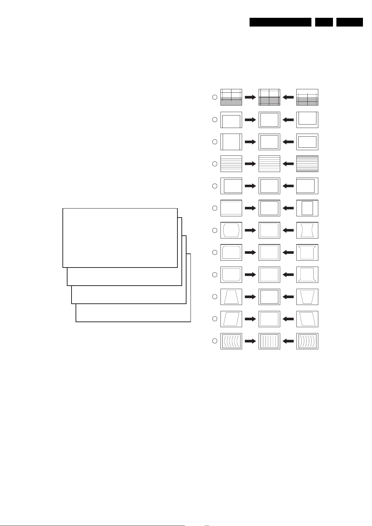
Alignments
A
GB 57L01.2A 8.
1. Activate the SAM.
2. Go to the TUNER sub menu.
3. Select AFW with the UP/DOWN cursor keys and set to
ON.
4. Select AGC with the UP/DOWN cursor keys.
5. Adjust the AGC-value (default value is 28) with the LEFT/
RIGHT cursor keys until the voltage at pin 1 of the tuner
lies between 3.8 and 2.3 V.
6. Select AFW with the UP/DOWN cursor keys and set to
OFF.
7. Switch the set to STANDBY.
YD (Y-delay)
Always set to 8.
CL (cathode drive level)
Always set to 7.
AFA
Read only bit, for monitoring purpose only.
AFB
Read only bit, for monitoring purpose only.
8.3.3 White Tone
– DELTA WARM G = -3
–DELTA WARM B = 2
8.3.4 Geometry
The geometry alignments menu contains several items to
align the set, in order to obtain correct picture geometry.
1
2
3
4
5
6
VERT. SLOPE
VERT. SHIFT
VERT. AMPLITUDE
V.S-CORRECTION
HOR. SHIFT
HOR. AMPLITUDE
SAM
NORM
COOL > (2)
WARM > (3)
(1) N O R M A L R E D X X
(2) D C O O L R E D X X
(3) D W A R M R E D X X
L > (1)
NORMAL GRE EN XX
NORMAL B LU E XX
DCOOLGREEN XX
DCOOLBLUE XX
DWARMGREEN XX
DWARM BLUE XX
CL 16532008_051.pdf
220501
Figure 8-8
In the WHITE TONE sub menu, the values of the black cut off
level can be adjusted. Normally, no alignment is needed for
the WHITE TONE. You can use the given default values.
The colour temperature mode (NORMAL, COOL and
WARM) and the colour (R, G, and B) can be selected with the
UP/DOWN RIGHT/LEFT cursor keys. The value can be
changed with the LEFT/RIGHT cursor keys. First, select the
values for the NORMAL colour temperature. Then select the
values for the COOL and WARM mode. After alignment,
switch the set to standby, in order to store the alignments.
Default settings:
1. NORMAL (colour temperature = 11500 K):
– NORMAL R = 32
– NORMAL G = 35
– NORMAL B = 30
2. COOL (colour temperature = 14000 K):
– DELTA COOL R = 0
– DELTA COOL G = -5
– DELTA COOL B = 5
3. WARM (colour temperature = 8200 K):
–DELTA WARM R = 8
7
8
9
10
11
12
Figure 8-9
Connect an external video pattern generator to the aerial
input of the TV-set and input a crosshatch test pattern. Set
the generator amplitude to at least 1 mV and set frequency to
475.25 MHz (PAL/SECAM) or 61.25 MHz (NTSC).
1. Set 'Smart Picture' to NATURAL (or MOVIES).
2. Activate the SAM menu (see chapter 5).
3. Go to the GEOMETRY sub menu.
4. Choose HORIZONTAL or VERTICAL alignment
Now you can perform the following alignments:
Horizontal:
• Horizontal Parallelogram (HP) Align straight vertical
lines in the top and the bottom; vertical rotation around
the centre.
• Horizontal Bow (HB) Align straight horizontal lines in
the top and the bottom; horizontal rotation around the
centre.
• Horizontal Shift (HSH) Align the horizontal centre of the
picture to the horizontal centre of the CRT.
E/W PARABOLE
UPPER E/W CORNER
LOWER E/W CORNER
E/W TRAPEZIUM
HOR. PARALLELOGRAM
HOR. BOW
CL 16532044_022.eps
140501
Page 32

GB 58 L01.2A8.
DEFAULT GEOMETRY VALUES (L01 SMALL SCREEN)
Alignment
Description
13V1414RF
15RF1719V2021
HP
Hor. Parallelogram 31 31 31 31 31 31 31 31
HB
Hor. Bow 3131313131313131
HSH
Hor. Shift 23 35233535233535
EWW
East West Width --------
EWP
East West Parabola - -------
UCP
Upper Corner Parabola - -------
LCP
Lower Corner Parabola - -------
EWT
East West Trapezium - -------
VSL
Vert. Slope 31 33 31 33 33 31 33 33
VAM
Vert. Amplitude 26 26 26 26 26 26 26 26
VSC
Vert. S-correction 23 23 23 23 23 23 23 23
VSH
Vert. Shift 3035303535 303535
VX
Vert. Zoom --------
H60
Hor. Shift offset (60 Hz) 09099099
V60
Vert. Shift offset (60 Hz) 0 -2 0 -2 -2 0 -2 -2
Abbreviations: V= visual, RF= Real Flat
CL 16532008_072.pdf
220801
AT XX
A F - M X X
A2T XX
QSS ON / OF F
FM I ON / O FF
CL 16532008_055.pdf
220501
See also Figure 8-9 numbers 11, 12 and 5.
HOR I ZON T AL >
VERT I CAL >
HP XX
HB XX
HSH X X
Alignments
SAM
CL 16532008_059.pdf
220501
Figure 8-10
Vertical:
• Vertical slope (VSL) Align the vertical centre of the
picture to the vertical centre of the CRT. This is the first
of the vertical alignments to perform. For an easy
alignment, set SBL to ON.
• Vertical Amplitude (VAM) Align the vertical amplitude
so that the complete test pattern is visible.
• Vertical S-Correction (VSC) Align the vertical
linearity, meaning that vertical intervals of a grid
pattern must be equal over the entire screen height.
• Vertical Shift (VSH) Align the vertical centring so that
the test pattern is located vertically in the middle. Repeat
the 'vertical amplitude' alignment if necessary.
• Service blanking (SBL) Switch the blanking of the lower
half of the screen ON or OFF (to be used in combination
with the vertical slope alignment).
• H60 Align straight horizontal lines if NTSC input (60 Hz)
is used i.s.o. PAL (50 Hz).
• V60 Align straight vertical lines if NTSC input (60 Hz) is
used i.s.o. PAL (50 Hz).
See also Figure 8-9 numbers 1, 3, 4 and 2.
Figure 8-12
8.3.5 Audio
SAM
Figure 8-13
No alignments are needed for the audio sub menu. Use the
given default values.
HOR I Z ONT AL >
VERT I CAL >
VSL XX
VAM XX
VSC XX
VSH XX
SBL ON/ OF F
VSX XX
H60 XX
In the table below, you will find the GEOMETRY default
values for the different sets.
V60 XX
Figure 8-11
SAM
CL 16532008_060.pdf
AT
Default value is 8.
AF-M
Default value is 44.
A2T
Default value is 250.
QSS
OFF for mono sets, ON for stereo sets.
FMI
OFF for mono sets, ON for stereo sets.
220501
Page 33

9. Circuit Description
Circuit Description
GB 59L01.2A 9.
Index:
1. Introduction
2. Audio Signal Processing
3. Video Signal Processing
4. Synchronisation
5. Deflection
6. Power Supply
7. Control
8. Abbreviations
Note:
• Figures can deviate slightly from the actual situation, due
to different set executions.
• For a good understanding of the following circuit
descriptions, please use the block diagram in chapter 6,
or the electrical diagrams in chapter 7. Where necessary,
you will find a separate drawing for clarification.
9.1 Introduction
The L01 (small screen) chassis is a global TV chassis for the
model year 2001 and is used for TV sets with screen sizes
from 14” - 21”. The standard architecture consists of a Main
panel, a Picture Tube panel, a Side (or Front) I/O panel and
a Front Control panel. The Main panel consists primarily of
conventional components with hardly any surface mounted
devices.
The L01 is divided into 2 basic systems, i.e. mono and stereo
sound. While the audio processing for the mono sound is
done in the audio block of the UOC, an external audio
processing IC is used for stereo sets.
The tuning system features 100 channels with on-screen
display. The main tuning system uses a tuner, a
microcomputer, and a memory IC mounted on the main
panel.
Also, in some type numbers, an FM radio is implemented
with 40 pre-set channels.
The microcomputer communicates with the memory IC, the
customer keyboard, remote receiver, tuner, signal processor
IC and the audio output IC via the I
retains the settings for favourite stations, customer-preferred
settings, and service/factory data.
The on-screen graphics and closed caption decoding are
done within the microprocessor, and then sent to the signal
processor IC to be added to the main signal.
The chassis uses a Switching Mode Power Supply (SMPS)
for the main voltage source. The chassis has a ‘hot’ ground
reference on the primary side and a cold ground reference on
the secondary side of the power supply and the rest of the
chassis.
2
C bus. The memory IC
9.2 Audio Signal Processing
Figure 9-1
The functions for video processing, microprocessor (m P) and
teletext (TXT) decoder are combined in one IC (TDA958xH),
the so-called Ultimate One Chip (UOC). This chip is (surface)
mounted on the copper side of the main panel.
9.2.1 Stereo
In stereo sets, the signal goes via the SAW filter (position
1004 in case of QSS demodulation and 1003 in case of
Intercarrier demodulation), to the audio demodulator part of
the UOC IC7200. The stereo audio output on pin 33 (or 38 for
QSS) goes, via TS7206 or (TS7201 for QSS), to the stereo
decoder 7831.
The switch inside the stereo decoder 7831 selects (via I
either the internal decoder or an external source.
The NICAM + 2CS AM/FM stereo decoder is an ITT
MSP34X5.
The output is fed to the to the audio amplifier (AN7522 at
position 7901). The volume level is controlled at this IC (pin
9) by a control line (VolumeMute) from the microprocessor.
The audio signal is then sent to the speaker/headphone
output panel.
2
C)
Figure 9-2
Page 34

GB 60 L01.2A9.
Circuit Description
FM ANT.
0265
RF ANT.
1000
11
POWER
SUPPLY
EXT. AUDIO
INPUT
TUNER
1
EXT. VIDEO
INPUT
AUDIO SOURCE SELECTION
FM FMR
10
11
AGC
VIDEO SOURCE
SELECTION
V
BAT
AUDIO
12V
3.9V
3.3V
7801
7209
7210
FM IF
BUFFER
SAW
FILTER
SAW
FILTER
1200 : 1202
SOUND
TRAP
INT_CVBS
EXT_CVBS
7802
7861
7831
CONTROL
AUDIO DECODING
AND
PROCESSING
SELECTION
47 24
MATR. SWITCH
7834
7200
SIF
23
24
VIF
18
19
22
38
40
42
VIDEO
SWITCH
33
SOUND
IF
DEMOD.
VISION
IF
DEMOD.
7835
µP
I2C
VIDEO
PROCESSING
SYNC
PROCESSING
16 17 15 30
25
RGB/YUV
PROCESSING
7901
AUDIO
AMPL.
EXT. AUDIO OUT
68
50:53
56:58
H
EW
V+
V-
7602
7330
7460
7471
NVM
VIDEO
AMPL.
HOR.
DEFL.
EW
VERT.
DEFL.
EHT
+
EXT RGB/YUV INPUT
9.2.2 Mono
In mono sets, the signal goes via the SAW filter (position
1004 in case of QSS demodulation and 1003 in case of
Intercarrier demodulation), to the audio demodulator part of
the UOC IC7200. The mono audio output on pin 48 goes
directly, via the smart sound circuit (7941 for Bass and 7942
EXT. AUDIO
OUTPUT
FM IF
FM FMR
BUFFER
SAW
FILTER
SAW
FILTER
FM ANT.
0265
RF ANT.
1000
11
EXT. AUDIO
INPUT
TUNER
1
10
11
AGC
CL 16532008_039.eps
220501
Figure 9-3
for Treble) and buffer (7943), to the audio amplifier (AN7523
at position 7902).
The volume level is controlled at this IC (pin 9) by a
‘VolumeMute’ control line from the microprocessor.
The audio signal is then sent to the speaker/headphone
output panel.
7941
7942
7943
SMART
SND
7200
SIF
23
24
18
19
22
SOUND
IF
DEMOD.
VIF
VISION
IF
DEMOD.
AUDIO SWITCH
µP
48
AVL
68
7902
AUDIO
AMPL.
9
VOLUME MUTE
7602
NVM
Figure 9-4
CL 16532008_040.eps
220501
Page 35

Circuit Description
GB 61L01.2A 9.
9.2.3 FM radio (if present)
The FM radio uses the 10.7 MHz concept. This SIF
frequency is available at pin 10 of the tuner. Via a preamplifier (TS7209 and TS7210), the signal is fed for
demodulation to either the UOC (for mono FM radio) or by the
Micronas MSP34X5 (for stereo FM radio).
9.3 Video Signal Processing
9.3.1 Introduction
The video signal-processing path consists of the following
parts:
• RF signal processing.
• Video source selection.
• Video demodulation.
• Luminance/Chrominance signal processing.
• RGB control.
• RGB amplifier
The processing circuits listed above are all integrated in the
UOC TV processor. The surrounding components are for the
adaptation of the selected application. The I
defining and controlling the signals.
9.3.2 RF Signal Processing
The incoming RF signal goes to the tuner (pos. 1000), where
the IF signal is developed and amplified. The IF signals then
exits the tuner from pin 11 to pass through the SAW filter
(position 1002 in case of QSS demodulation and 1003 in
case of Intercarrier demodulation). The shaped signal is then
applied to the IF processor part of the UOC (pos. 7200).
Tuner AGC (Automatic Gain Control) will reduce the tuner
gain and thus the tuner output voltage when receiving strong
RF signals. Adjust the AGC take-over point via the Service
Alignment Mode (SAM). The tuner AGC starts working when
the video-IF input reaches a certain input level and will adjust
this level via the I
tuner (pin 1) via the open collector output (pin 22) of the UOC.
The IC also generates an Automatic Frequency Control
(AFC) signal that goes to the tuning system via the I
to provide frequency correction when needed.
The demodulated composite video signal is available at pin
38 and then buffered by transistor 7201.
9.3.3 Video Source Selection
The Composite Video Blanking Signal (CVBS) from buffer
7201 goes to the audio carrier trap filters (1200, 1201, or
1202 depending on the system used) to remove the audio
signal. The signal then goes to pin 40 of IC7200. The internal
input switch selects the following input signals:
• Pin 40: terrestrial CVBS input
• Pin 42: external AV1 CVBS input
• Pin 44: external Side I/O CVBS or AV2 Luminance (Y)
input
• Pin 45: external AV2 Chrominance (C) input
2
C bus. The tuner AGC signal goes to the
2
C bus is for
2
C bus,
7200
UOC
RGB/YUV _IN
AV1_CVBS1_1
CVBS_FRONT_IN
AV2 CVBS_IN
SVHS
Y_IN
C_IN
0225-B
FRONT AUDIO IN
AV1 AUDIO IN
AV1 AUDIO IN
INTERNAL_CVBS_IN
1, 12
5, 14
2, 15
7802
7801
SY_CVBS_IN
9
SEL-MAIN-FRNT-RR
SC2-CTRL
910
3, 13
51 53
C-IN 45
SC1-IN
41, 42
40
42
44
70
4
7831
QSS_AM_DEM_OUT
47
SOUND
DEC
RGB/YUV
INSERT
VIDEO
PROC.
P
Figure 9-5
Once the signal source is selected, a chroma filter calibration
is performed. The received colour burst sub-carrier
frequency is used for this. Correspondingly, the chroma band
pass filter for PAL/NTSC processing or the cloche filter for
SECAM processing is switched on. The selected luminance
(Y) signal is supplied to the horizontal and vertical
synchronisation processing circuit and to the luminance
processing circuit. In the luminance-processing block, the
luminance signal goes to the chroma trap filter. This trap is
switched 'on' or 'off' depending on the colour burst detection
of the chroma calibration circuit.
The group delay correction part can be switched between the
BG and a flat group delay characteristic. This has the
advantage that in multi-standard receivers no compromise
has to be made for the choice of the SAW filter.
9.3.4 Video Demodulation
The colour decoder circuit detects whether the signal is a
PAL, NTSC or SECAM signal. The result is made known to
the auto system manager. The PAL/NTSC decoder has an
internal clock generator, which is stabilised to the required
frequency by using the 12 MHz clock signal from the
reference oscillator of the microcontroller/teletext decoder.
The base-band delay line is used to obtain a good
suppression of cross colour effects.
The Y signal and the delay line outputs U and V are applied
to the luminance/chroma signal processing part of the TV
processor.
9.3.5 Luminance/Chrominance signal Processing
The output of the YUV separator is fed to the internal YUV
switch, which switches between the output of the YUV
separator or the external YUV (for DVD or PIP) on pins 51-
53. Pin 50 is the input for the insertion control signal called
‘FBL-1’. When this signal level becomes higher than 0.9 V
(but less than 3 V), the RGB signals at pins 51, 52 and 53 are
inserted into the picture by using the internal switches.
Also some picture improvement features are implemented in
this part:
• Black stretch. This function corrects the black level of
incoming signals, which have a difference between the
black level and the blanking level. The amount of
extension depends upon the difference between actual
black level and the darkest part of the incoming video
signal level. It is detected by means of an internal
capacitor.
• White stretch. This function adapts the transfer
characteristic of the luminance amplifier in a non-linear
RGB
56 58
V-OUT
47
L/R OUT
30, 31
MAIN_OUT
24,25
CL 16532016_011.eps
MON. OUT
7901
CRT
PANEL
AUDIO
AMPL.
120401
Page 36

GB 62 L01.2A9.
Circuit Description
way depending on the average picture content of the
luminance signal. It operates in such a way that
maximum stretching is obtained when signals with a low
video level are received. For bright pictures, stretching is
not active.
• Dynamic skin tone correction. This circuit corrects
(instantaneously and locally) the hue of those colours
which are located in the area in the UV plane that
matches the skin tone. The correction is dependent on
the luminance, saturation and distance to the preferred
axis.
The YUV signal is then fed to the colour matrix circuit, which
converts it to R, G and B signals.
The OSD/TXT signal from the microprocessor is mixed with
the main signal at this point, before being output to the CRT
board (pins 56, 57 and 58).
9.3.6 RGB Control
The RGB control circuit enables the picture parameters
contrast, brightness and saturation to be adjusted, by using
a combination of the user menus and the remote control.
Additionally automatic gain control for the RGB signals via
cut-off stabilisation is achieved in this functional block to
obtain an accurate biasing of the picture tube. Therefor this
block inserts the cut-off point measuring pulses into the RGB
signals during the vertical retrace period.
The following additional controls are used:
• Black current calibration loop. Because of the 2-point
black current stabilisation circuit, both the black level and
the amplitude of the RGB output signals depend on the
drive characteristics of the picture tube. The system
checks whether the returning measuring currents meet
the requirements, and adapt the output level and gain of
the circuit when necessary. After stabilisation of the loop,
the RGB drive signals are switched on. The 2-point black
level system adapts the drive voltage for each cathode in
such a way that the two measuring currents have the
right value. This is done with the measurement pulses
during the frame flyback. During the first frame, three
pulses with a current of 8 m A are generated to adjust the
cut off voltage. During the second frame, three pulses
with a current of 20 mA are generated to adjust the ‘white
drive’. This has as a consequence, that a change in the
gain of the output stage will be compensated by a gain
change of the RGB control circuit. Pin 55 (BLKIN) of the
UOC is used as the feedback input from the CRT base
panel.
• Blue stretch. This function increases the colour
temperature of the bright scenes (amplitudes which
exceed a value of 80% of the nominal amplitude). This
effect is obtained by decreasing the small signal gain of
the red and green channel signals, which exceed this
80% level.
• Beam current limiting. A beam current limiting circuit
inside the UOC handles the contrast and brightness
control for the RGB signals. This prevents the CRT from
being overdriven, which could otherwise cause serious
damage in the line output stage. The reference used for
this purpose is the DC voltage on pin 54 (BLCIN) of the
TV processor. Contrast and brightness reduction of the
RGB output signals is therefore proportional to the
voltage present on this pin. Contrast reduction starts
when the voltage on pin 54 is lower than 2.8 V.
Brightness reduction starts when the voltage on pin 54 is
less than 1.7 V. The voltage on pin 54 is normally 3.3 V
(limiter not active). During set switch-off, the black
current control circuit generates a fixed beam current of
1 mA. This current ensures that the picture tube
capacitance is discharged. During the switch-off period,
the vertical deflection is placed in an over-scan position,
so that the discharge is not visible on the screen.
9.3.7 RGB Amplifier
From outputs 56, 57 and 58 of IC7200, the RGB signals are
applied to the analogue output amplifiers on the CRT panel.
The R-signal is amplified by a circuit built around transistors
TS7311, 7312 and 7313, which drives the picture tube
cathodes. For the other two signals see the blockdiagram in
chapter 6.
The supply voltage for the amplifier is +160 V and is derived
from the line output stage.
9.4 Synchronisation
Inside IC7200 (part D), the vertical and horizontal syncpulses are separated. These ‘H’ and ‘V’ signals are
synchronised with the incoming CVBS signal. They are then
fed to the H- and V-drive circuits and to the OSD/TXT circuit
for synchronisation of the On Screen Display and Teletext
(or Closed Caption) information.
9.5 Deflection
9.5.1 Horizontal Drive
The horizontal drive signal is obtained from an internal VCO,
which is running at twice the line frequency. This frequency
is divided by two, to lock the first control loop to the incoming
signal.
When the IC is switched ‘on’, the ‘Hdrive’ signal is
suppressed until the frequency is correct.
The ‘Hdrive’ signal is available at pin 30. The ‘Hflybk’ signal
is fed to pin 31 to phase lock the horizontal oscillator, so that
TS7401 cannot switch ‘on’ during the flyback time.
When the set is switched on, the ‘+8V’ voltage goes to pin 9
of IC7200. The horizontal drive starts up in a soft start mode.
It starts with a very short T
transistor. The T
normal operation. The starting frequency during switch on is
therefore about 2 times higher than the normal value. The
‘on’ time is slowly increased to the nominal value in 1175 ms.
When the nominal value is reached, the PLL is closed in such
a way that only very small phase corrections are necessary.
The ‘EHTinformation’ line on pin 11 is intended to be used as
a ‘X-ray’ protection. When this protection is activated (when
the voltage exceeds 6 V), the horizontal drive (pin 30) is
switched 'off' immediately. If the ‘H-drive’ is stopped, pin 11
will become low again. Now the horizontal drive is again
switched on via the slow start procedure.
The ‘EHTinformation’ line (Aquadag) is also fed back to the
UOC IC7200 pin 54, to adjust the picture level in order to
compensate for changes in the beam current.
The filament voltage is monitored for ‘no’ or ‘excessive’
voltage. This voltage is rectified by diode 6413 and fed to the
emitter of transistor TS7405. If this voltage goes above 6.8 V,
TS7405 will conduct, making the ‘EHT0’ line ‘high’. This will
immediately switch off the horizontal drive (pin 30) via the
slow stop procedure.
The horizontal drive signal exits IC7200 at pin 30 and goes to
TS7401, the horizontal driver transistor. The signal is
amplified and coupled to the base circuit of TS7402, the
horizontal output transistor. This will drive the line output
transformer (LOT) and associated circuit. The LOT provides
the extra high voltage (EHT), the VG2 voltage and the focus
and filament voltages for the CRT, while the line output circuit
drives the horizontal deflection coil.
of the transistor is identical to the time in
OFF
time of the horizontal output
ON
Page 37

9.5.2 Vertical Drive
A divider circuit performs the vertical synchronisation. The
vertical ramp generator needs an external resistor (R3245,
pin 20) and capacitor (C2244, pin 21). A differential output is
available at pins 16 and 17, which are DC-coupled with the
vertical output stage.
To avoid damage of the picture tube when the vertical
deflection fails, the ‘V_GUARD’ output is fed to the beam
current limiting input. When a failure is detected, the RGBoutputs are blanked. When no vertical deflection output stage
is connected, this guard circuit will also blank the output
signals.
These ‘V_DRIVE+’ and ‘V_DRIVE-‘ signals are applied to the
input pins 7 and 1 of IC7471 (vertical deflection amplifier).
These are voltage driven differential inputs. As the driver
device (IC7200) delivers output currents, R3474 and R3479
convert them to voltage. The differential input voltage is
compared with the voltage across measuring resistor R3471
that provides internal feedback information. The voltage
across this measuring resistor is proportional to the output
current, which is available at pin 5 where it drives the vertical
deflection coil (connector 0222).
IC7471 is supplied by +/-13 V. The vertical flyback voltage is
generated at pin 3.
9.6 Power Supply
V
LINE
V
IN
C
IN
V
CC
TEA1507
Vcc Drain
1
Gnd
2
Ctrl
3
Demag4
Driver
Sense
8
HVS
7
6
5
N
P
N
S
C
D
C
SS
R
SS
R
SENSE
N
Vcc
Circuit Description
1
V
CC
2
GND
3
CTRL
9.6.1 Introduction
V
OUT
GB 63L01.2A 9.
I
ss
0.5 V
soft
start
S2
CL 16532020_073.eps
060701
8
7
4
6
5
2.5 V
S1
TEA1507
M-level
burst
detect
SUPPLY
MANAGEMENT
internal
UVLO start
supply
VOLTAGE
CONTROLLED
OSCILLATOR
FREQUENCY
CONTROL
OVER-
TEMPERATURE
PROTECTION
−1
POWER-ON
RESET
UVLO
MAXIMUM
ON-TIME
PROTECTION
LOGIC
LOGIC
SQ
R
START-UP
CURRENT SOURCE
VALLEY
Q
short
winding
100 mV
PROTECTION
DRIVER
LEB
blank
OCP
OVER-
VOLTAGE
0.75 V
clamp
OVERPOWER
PROTECTION
Figure 9-7
The supply is a Switching Mode Power Supply (SMPS). The
frequency of operation varies with the circuit load. This
‘Quasi-Resonant Flyback’ behaviour has some important
benefits compared to a ‘hard switching’ fixed frequency
Flyback converter. The efficiency can be improved up to
90%, which results in lower power consumption. Moreover
the supply runs cooler and safety is enhanced.
The power supply starts operating when a DC voltage goes
from the rectifier bridge via T5520, R3532 to pin 8. The
operating voltage for the driver circuit is also taken from the
‘hot’ side of this transformer.
The switching regulator IC 7520 starts switching the FET ‘on’
and ‘off’, to control the current flow through the primary
winding of transformer 5520. The energy stored in the
primary winding during the ‘on’ time is delivered to the
secondary windings during the ‘off’ time.
The ‘MainSupply’ line is the reference voltage for the power
supply. It is sampled by resistors 3543 and 3544 and fed to
the input of the regulator 7540 / 6540. This regulator drives
the feedback optocoupler 7515 to set the feedback control
voltage on pin 3 of 7520.
The power supply in the set is ‘on’ any time AC power goes
to the set.
DRAIN
HVS
n.c.
DEM
DRIVER
I
sense
Figure 9-6
CL 16532020_074.eps
120401
Derived Voltages
The voltages supplied by the secondary windings of T5520
are:
• ‘MainAux’ for the audio circuit (voltage depends on set
execution, see table below),
• 3.3 V and 3.9 V for the microprocessor and
• ‘MainSupply’ for the horizontal output (voltage depends
on set execution, see table below).
Other supply voltages are provided by the LOT. It supplies
+50 V (only for large screen sets), +13 V, +8 V, +5 V and a
+200 V source for the video drive. The secondary voltages of
the LOT are monitored by the ‘EHTinformation’ lines. These
lines are fed to the video processor part of the UOC IC 7200
on pins 11 and 34.
This circuit will shut ‘off’ the horizontal drive in case of overvoltage or excessive beam current.
Page 38

GB 64 L01.2A9.
Circuit Description
Mains AC
Input
A1
Degaussing
Control
Circuit
A1
Main
Power
Supply
+3.9V +3.3V
Main Supply
Main Aux
3V3 Reg.
V
IN
C
EHT
A2
Focus
VG2
VideoSupply
Filament
Lot
VlotAux +13V
VlotAux -13V
*VlotAux +50V
VlotAux +5V
+8V
VT_Supply
+6.8V
B1/B2
CRT
Panel
A15
Tilt&
Rotation
A1
Degaussing
Circuit
A2
EW
Correction
A2
Horizontal
Deflection
A3
Frame
Deflection
A4
Tuner
A7
uP
A5
Video
Processing
A9
Sound
Processing
A11
A8
Audio
Amplifier
A10
Source
Selection
Switch
CL 16532008_004.eps
Vaux
+3.3V
+3.9V
Vaux
250401
V
GATE
V
D
I
L
I
IN
V
GATE
L
L
P
D
C
OUT
n⋅V
OUT
V
D
C
D
n⋅V
OUT
Valley
V
IN
0
Magnetization
0
t
0
Demagneti-
zation
3
2
1
t
t
2
1
T
4
t
3
CL 16532020_084.eps
t
00
110401
Figure 9-8
Figure 9-9
Degaussing
When the set is switched on, the degaussing relay 1515 is
immediately activated as transistor 7580 is conducting. Due
to the RC-time of R3580 and C2580, it will last about 3 to 4
seconds before transistor 7580 is switched off.
9.6.2 Basic IC Functionality
For a clear understanding of the Quasi-Resonant behaviour,
it is possible to explain it by a simplified circuit diagram (see
Figure below). In this circuit diagram, the secondary side is
transferred to the primary side and the transformer is
replaced by an inductance L
. CD is the total drain
P
capacitance including the resonance capacitor C
output capacitor C
capacitance C
transformer is represented by n (N
of the MOSFET and the winding
OSS
of the transformer. The turns ratio of the
W
P/NS
).
CL 16532008_063.pdf
230501
, parasitic
R
Figure 9-10
In the Quasi-Resonant mode each period can be divided into
four different time intervals, in chronological order:
• Interval 1: t0 < t < t1 primary stroke At the beginning of
the first interval, the MOSFET is switched ‘on’ and
energy is stored in the primary inductance
(magnetisation). At the end, the MOSFET is switched
‘off’ and the second interval starts.
• Interval 2: t1 < t < t2 commutation time In the second
interval, the drain voltage will rise from almost zero to
V
+n•(V
IN
+VF). VF is the forward voltage drop of de
OUT
diode that will be omitted from the equations from now
on. The current will change its positive derivative,
corresponding to V
corresponding to -n•V
, to a negative derivative,
IN/LP
/LP.
OUT
• Interval 3: t2 < t < t3 secondary stroke In the third interval,
the stored energy is transferred to the output, so the
diode starts to conduct and the inductive current I
will
L
decrease. In other words, the transformer will be
demagnetised. When the inductive current has become
zero the next interval begins.
• Interval 4: t3 < t < t00 resonance time In the fourth
interval, the energy stored in the drain capacitor C
start to resonate with the inductance L
. The voltage and
P
will
D
current waveforms are sinusoidal waveforms. The drain
voltage will drop from V
IN
+n•V
to VIN-n•V
OUT
OUT
.
Frequency Behaviour
The frequency in the QR-mode is determined by the power
stage and is not influenced by the controller (important
parameters are L
input voltage V
and CD). The frequency varies with the
P
and the output power P
IN
. If the required
OUT
output power increases, more energy has to be stored in the
transformer. This leads to longer magnetising t
demagnetising t
times, which will decrease the frequency.
SEC
PRIM
and
See the frequency versus output power characteristics
below. The frequency characteristic is not only output power, but also input voltage dependent. The higher the input
voltage, the smaller t
, so the higher the frequency will be.
PRIM
Page 39

f
switching
frequency
f
MIN
P2
MAX
V
IN_MAX
V
IN_MIN
P
OUT_MIN
QR frequency characteristics at different input voltages
P
power
CL 16532020_077.eps
P1
OUT_MAX
100401
Figure 9-11
Point P1 is the minimum frequency f
that occurs at the
MIN
specified minimum input voltage and maximum output power
required by the application. Of course the minimum
frequency has to be chosen above the audible limit (>20
kHz).
Start-Up Sequence
When the rectified AC voltage V
(via the centre tap
IN
connected to pin 8) reaches the Mains dependent operation
level (Mlevel: between 60 and 100 V), the internal ‘Mlevel
switch’ will be opened and the start-up current source is
enabled to charge capacitor C2521 at the V
pin as shown
CC
below.
The ‘soft start’ switch is closed when the V
of 7 V and the ‘soft start’ capacitor C
SS
reaches a level
CC
(C2522, between pin
5 and the sense resistor R3526), is charged to 0.5 V.
Once the V
V
CC-start
capacitor is charged to the start-up voltage
CC
(11 V), the IC starts driving the MOSFET. Both
internal current sources are switched ‘off’ after reaching this
start-up voltage. Resistor R
(3524) will discharge the ‘soft
SS
start’ capacitor, such that the peak current will slowly
increase. This to prevent ‘transformer rattle’.
During start-up, the V
capacitor will be discharged until the
CC
moment that the primary auxiliary winding takes over this
voltage.
V
IN
I
1
charged
in(Vcc)
8
I
Mlevel
SS
0.5V
soft start
V
R
SENSE
SS
5
C
+
V
OCP
-
2
SS
I
L
R
SENSE
Start-up sequence
V
=11V
(start)
≈
7V
τ
Charging of VCC capacitor
taken over by the windin g
⋅
= R
C
SS
SS
V
C
Vcc
C
by current
I
V
CC
V
Vcc
V
L
V
CC
SENSE
OUT
GATE
Circuit Description
The moment that the voltage on pin 1 drops below the ‘under
voltage lock out‘ level (UVLO = ± 9 V), the IC will stop
switching and will enter a safe restart from the rectified mains
voltage.
Operation
The supply can run in three different modes depending on
the output power:
• Quasi-Resonant mode (QR) The QR mode, described
above, is used during normal operation. This will give a
high efficiency.
• Frequency Reduction mode (FR) The FR mode (also
called VCO mode) is implemented to decrease the
switching losses at low output loads. In this way the
efficiency at low output powers is increased, which
enables power consumption smaller than 3 W during
stand-by. The voltage at the pin 3 (Ctrl) determines
where the frequency reduction starts. An external Ctrl
voltage of 1.425 V corresponds with an internal VCO
level of 75 mV. This fixed VCO level is called V
The frequency will be reduced in relation to the VCO
voltage between 75 mV and 50 mV (at levels larger than
75 mV, Ctrl voltage < 1.425V, the oscillator will run on
maximum frequency f
(V
of 6 kHz. Valley switching is still active in this mode.
• Minimum Frequency mode (MinF) At VCO levels below
50 mV, the minimum frequency will remain on 6 kHz,
which is called the MinF mode. Because of this low
frequency, it is possible to run at very low loads without
having any output regulation problems.
= 175 kHz
f
oscH
kH
switching
frequency
f
= 6 kHz
oscL
Safe-Restart Mode
This mode is introduced to prevent the components from
being destroyed during eventual system fault conditions. It is
also used for the Burst mode. The Safe-Restart mode will be
entered if it is triggered by one of the following functions:
• Over voltage protection,
• Short winding protection,
• Maximum ‘on time’ protection,
•V
• Detecting a pulse for Burst mode,
• Over temperature protection.
When entering the Safe-Restart mode, the output driver is
immediately disabled and latched. The V
charge the V
drop until UVLO is reached. To recharge the V
the internal current source (I
to initiate a new start-up sequence as described before. This
Safe-Restart mode will persist until the controller detects no
faults or burst triggers.
GB 65L01.2A 9.
= 175 kHz typically). At 50 mV
) the frequency is reduced to the minimum level
VCO,max
MinF FR QR
reaching UVLO level (fold back during overload),
CC
capacitor anymore and the VCC voltage will
CC
oscH
V
VCO,start
V
VCO,max
P
OUT_MIN
Multi mode operation
Figure 9-13
(restart)(VCC)
frequency limit
P
power
CL 16532020_080.eps
winding will not
CC
capacitor,
CC
) will be switched ‘on’
VCO,start
OUT_MAX
100401
.
Figure 9-12
CL 16532020_078.eps
110401
Standby
The set goes to Standby in the following cases:
• After pressing the ‘standby’ key on the remote control.
Page 40

GB 66 L01.2A9.
R
1
R
2
D
V
CC
windi ng
I
(ovp)(demag)
I
(opp)(demag)
Demag4
Ctrl
Gn
d
Vcc Drain
HVS
Driver
Sens
3
2
1
5
6
7
8
configurat ion
A
B
0V
OUT
S
Vcc
V
N
N
⋅
IN
P
Vcc
V
N
N
⋅
Demagnetization
V
GATE
V
WINDING
Magnetization
V
demag
Comparator
threshold
V
demag
0.7V
0V
-0.25V
Circuit Description
• When the set is in protection mode.
In Standby, the power supply works in ‘burst mode’.
Burst mode can be used to reduce the power consumption
below 1 W at stand-by. During this mode, the controller is
active (generating gate pulses) for only a short time and for a
longer time inactive waiting for the next burst cycle.
In the active period the energy is transferred to the secondary
and stored in the buffer capacitor C
in front of the linear
STAB
stabiliser (see Figure below). During the inactive period, the
load (e.g. microprocessor) discharges this capacitor. In this
mode, the controller makes use of the Safe-Restart mode.
V
IN
V
CC
Vcc Drain
1
C
Vcc
2
3
Gnd
Ctrl
Demag4
Driver
Sense
8
7
HVS
6
5
R
1
Basic Burst mode con figuration
V
STAB
C
STAB
Burst-Mode stand-by on/off
from microprocessor
Current pulse
generator
Figure 9-14
The system enters burst mode standby when the
microprocessor activates the ‘Stdby_con’ line. When this line
is pulled high, the base of Q7541 is allowed to go high. This
is triggered by the current from collector Q7542. When
Q7541 turns ‘on’, the opto-coupler (7515) is activated,
sending a large current signal to pin 3 (Ctrl). In response to
this signal, the IC stops switching and enters a ‘hiccup’ mode.
This burst activation signal should be present for longer than
the ‘burst blank’ period (typically 30 ms): the blanking time
prevents false burst triggering due to spikes.
Burst mode standby operation continues until the
microcontroller pulls the ‘Stdby_con’ signal low again. The
base of Q7541 is unable to go high, thus cannot turn ‘on’.
This will disable the burst mode. The system then enters the
start-up sequence and begins normal switching behaviour.
For a more detailed description of one burst cycle, three time
intervals are defined:
• t1: Discharge of V
when gate drive is active During the
CC
first interval, energy is transferred, which result in a
ramp-up of the output voltage (V
) in front of the
STAB
stabiliser. When enough energy is stored in the
capacitor, the IC will be switched ‘off’ by a current pulse
generated at the secondary side. This pulse is
transferred to the primary side via the opto coupler. The
controller will disable the output driver (safe restart
mode) when the current pulse reaches a threshold level
of 16 mA into the Ctrl pin. A resistor R
(R3519) is placed
1
in series with the opto coupler, to limit the current going
into the Ctrl pin. Meanwhile the V
discharged but has to stay above V
• t2: Discharge of V
when gate drive is inactive During
CC
the second interval, the V
CC
capacitor is
CC
UVLO
is discharged to V
output voltage will decrease depending on the load.
• t3: Charge of V
when gate drive is inactive The third
CC
interval starts when the UVLO is reached. The internal
current source charges the V
start capacitor is recharged). Once the V
charged to the start-up voltage, the driver is activated
and a new burst cycle is started.
capacitor (also the soft
CC
Linear
stabilizer
CL 16532020_081.eps
.
UVLO
capacitor is
CC
V
µ
C
100401
. The
t2
Active/
inactive
I
L
V
STAB
V
CC
t1
Burst mode waveforms
t3
Soft start
CL 16532020_082.eps
Figure 9-15
9.6.3 Protection Events
The SMPS IC 7520 has the following protection features:
Demagnetisation sense
This feature guarantees discontinuous conduction mode
operation in every situation. The oscillator will not start a new
primary stroke until the secondary stroke has ended. This is
to ensure that FET 7521 will not turn on until the
demagnetisation of transformer 5520 is completed. The
function is an additional protection feature against:
• saturation of the transformer,
• damage of the components during initial start-up,
• an overload of the output.
The demag(netisation) sense is realised by an internal circuit
that guards the voltage (Vdemag) at pin 4 that is connected
winding by resistor R1 (R3522). The Figure below
to V
CC
shows the circuit and the idealised waveforms across this
winding.
e
Figure 9-16
Over Voltage Protection
The Over Voltage Protection ensures that the output voltage
will remain below an adjustable level. This works by sensing
the auxiliary voltage via the current flowing into pin 4 (DEM)
during the secondary stroke. This voltage is a well-defined
replica of the output voltage. Any voltage spikes are
averaged by an internal filter.
If the output voltage exceeds the OVP trip level, the OVP
circuit switches the power MOSFET ‘off’.
Next, the controller waits until the ‘under voltage lock out‘
level (UVLO = ± 9 V) is reached on pin 1 (V
followed by a safe restart cycle, after which switching starts
again. This process is repeated as long as the OVP condition
exists. The output voltage at which the OVP function trips, is
set by the demagnetisation resistor R3522.
Over Current Protection
The internal OCP protection circuit limits the ‘sense’ voltage
on pin 5 to an internal level.
V
µC
V
(start)
V
(UVLO)
100401
). This is
CC
Page 41

Circuit Description
GB 67L01.2A 9.
Over Power Protection
During the primary stroke, the rectified AC input voltage is
measured by sensing the current drawn from pin 4 (DEM).
This current is dependent on the voltage on pin 9 of
transformer 5520 and the value of R3522. The current
information is used to adjust the peak drain current, which is
measured via pin I
SENSE
.
Short Winding Protection
If the ‘sense’ voltage on pin 5 exceeds the short winding
protection voltage (0.75 V), the converter will stop switching.
Once V
drops below the UVLO level, capacitor C2521 will
CC
be recharged and the supply will start again. This cycle will
be repeated until the short circuit is removed (safe restart
mode). The short winding protection will also protect in case
of a secondary diode short circuit.
This protection circuit is activated after the leading edge
blanking time (LEB).
LEB time
The LEB (Leading Edge Blanking) time is an internally fixed
delay, preventing false triggering of the comparator due to
current spikes. This delay determines the minimum ‘on’ time
of the controller.
Over Temperature protection
When the junction temperature exceeds the thermal
shutdown temperature (typ. 140º C), the IC will disable the
driver. When the V
capacitor will be recharged to the V
temperature is still too high, the V
voltage drops to UVLO, the VCC
CC
level. If the
(start)
voltage will drop again to
CC
the UVLO level (Safe-Restart mode). This mode will persist
until the junction temperature drops 8 degrees typically below
the shutdown temperature.
Mains dependent operation enabling level
To prevent the supply from starting at a low input voltage,
which could cause audible noise, a mains detection is
implemented (Mlevel). This detection is provided via pin 8,
that detects the minimum start-up voltage between 60 and
100 V. As previous mentioned, the controller is enabled
between 60 and 100 V.
An additional advantage of this function is the protection
against a disconnected buffer capacitor (C
the supply will not be able to start-up because the V
). In this case,
IN
CC
capacitor will not be charged to the start-up voltage.
9.7.1 Introduction
The microprocessor part of the UOC, has the complete
control and teletext on board. User menu, Service Default
Mode, Service Alignment Mode and Customer Service Mode
are generated by the mP. Communication to other ICs is done
2
2
C-Bus
C-bus.
via the I
9.7.2 I
The main control system, which consists of the
microprocessor part of the UOC (7200), is linked to the
external devices (tuner, NVM, MSP, etc) by means of the I
bus. An internal I
2
C-bus is used to control other signal
processing functions, like video processing, sound IF, vision
IF, synchronisation, etc.
9.7.3 User Interface
There are two control signals, called ‘KEYBOARD_protn’ and
‘IR’. Users can interact either through the Remote Control
transmitter, or by activation of the appropriate keyboard
buttons.
The L01 uses a remote control with RC5 protocol. The
incoming signal is connected to pin 67 of the UOC.
The 'Top Control' keyboard, connected to UOC pin 80, can
also control the set. Button recognition is done via a voltage
divider.
The front LED (6691) is connected to an output control line of
the microprocessor (pin 5). It is activated to provide the user
information about whether or not the set is working correctly
(e.g., responding to the remote control or fault condition)
9.7.4 Sound Interface
There are three control signals, called ‘Volume_Mute’,
‘Treble_Buzzer_Hosp_app’ and ‘Bass_panorama’.
The ‘Volume_Mute’ line controls the sound level output of the
audio amplifier or to mute it in case of no video identification
or from user command. This line also controls the volume
level during set switch ‘on’ and ‘off’ (to prevent audio plop).
The ‘Treble’ and ‘Bass’ lines are used (in mono 4:3 sets) to
switch between different smart sound modes.
2
C-
9.7 Control
User
Interface
Deflection
16:9
Sound
Amplifier
Processing
Tilt
ITV
Pip
Expansion
Slot
9.7.5 In- and Output Selection
For the control of the input and output selections, there are
Signal
Processing
LED
IR
KEYBOARD/
(EW protection
PANORAMA
VOLUME/
MUTE
TREBLE/Tilt
BASS
BUZZ
PANORAMA
ITV-DATA-OUT
or
ITV-DATA-IN
ITV-CLOCK
RESET
uP - Control
internal I2C Bus
STATUS 1
STATUS 2
SEL-MAIN-FRNT-RR
POWER_DOWN
STBY_CON
WRITE Enable
SEL-IF-LL/M-TRAP
I2C Bus
I/O
Power
Supply
NVM
Tuner / IF
CL 16532016_015.eps
220301
three lines:
• STATUS1 This signal provides information to the
microprocessor on whether a video signal is available on
the SCART1 AV input and output port (only for Europe).
This signal is not connected in NAFTA sets.
• STATUS2 This signal provides information to the
microprocessor on whether a video signal is available on
the SCART2 AV input and output port (only for Europe).
For sets with an SVHS input it provides the additional
information if a Y/C or CVBS source is present. The
presence of an external Y/C source makes this line ‘high’
while a CVBS source makes the line ‘low’.
• SEL-MAIN-FRNT-RR This is the source select control
signal from the microprocessor. This control line is under
user control or can be activated by the other two control
lines.
9.7.6 Power Supply Control
The microprocessor part is supplied with 3.3 V and 3.9 V both
derived from the ‘MainAux’ voltage via a 3V3 stabiliser (7560)
and a diode.
Figure 9-17
Two signals are used to control the power supply:
Page 42

GB 68 L01.2A9.
Circuit Description
• Stdby_con This signal is generated by the
microprocessor when over-current takes place at the
‘MainAux’ line. This is done to enable the power supply
into standby burst mode, and to enable this mode during
a protection. This signal is ‘low’ under normal operation
conditions and goes to ‘high’ (3.3 V) under ‘standby’ and
‘fault’ conditions.
• POWER_DOWN This signal is generated by the power
supply. Under normal operating conditions this signal is
‘high’ (3.3 V). During ‘standby’ mode, this signal is a
pulse train of approx. 10 Hz and a ‘high’ duration of 5 ms.
It is used to give information to the UOC about the fault
condition in the Audio amplifier supply circuit. This
information is generated by sensing the current on the
‘MainAux’ line (using voltage drop across R3564 to
trigger TS7562). This signal goes ‘low’ when the DCcurrent on the ‘MainAux’ line exceeds 1.6 - 2.0 A. It is
also used to give an early warning to the UOC about a
power failure. Then the information is used to mute the
sound amplifier to prevent a switch off noise and to solve
the switch-off spot.
9.7.7 Tuner IF
Pin 3 of the UOC (SEL-IF-LL’_M-TRAP), is an output pin to
switch the SAW-filter to the appropriate system.
• If UOC pin 3 is ‘low’, the selected system is:
– West Europe: PAL B/G, I, SECAM L/L’
– East Europe: PAL B/G
– Asia Pacific: NTSC M
• If UOC pin 3 is ‘high’, the selected system is:
– West Europe: SECAM L’, L’-NICAM
– East Europe: PAL D/K
– Asia Pacific: PAL B/G, D/K, I
9.7.8 Protection Events
Several protection events are controlled by the UOC:
• BC protection, to protect the picture tube from a too high
beam current. The UOC has the capability of measuring
the normal back level current during the vertical flyback.
So if for some reason the CRT circuit is malfunctioning
(i.e. high beam current), the normal black current will be
out of the 75 mA range, and the UOC will trigger the
power supply to shut down. However, this is a high
beam-current situation, the TV screen will be bright white
before the set is shut down.
• E/W protection, two protection mechanisms are built in,
over-current and over-voltage.
– In case of over-current due to defective parts in the
line deflection output stage, a high current will flow
through resistors 3405//3406. If this current is large
enough to create a voltage drop of 0.7 V across
3405//3406, transistor TS7606 (in A7 diagram) will
conduct and pin 80 of the UOC will be pulled down.
Thereafter, the UOC will shut down the power
supply. In case of further current increase, the fused
resistor 3411 is built-in for double protection.
– In case of a high voltage appearing across capacitor
2401 (dependent of the tube size), which is high
enough to trigger zener diode 6401 into conduction,
transistor TS7606 (in A7 diagram) will conduct and
UOC is triggered to shut down the power supply.
• I2C protection, to check whether all I
functioning.
In case one of these protections is activated, the set will go
into ‘standby’.
The ‘on’ and ‘standby’ LEDs are controlled via the UOC.
2
C IC's are
9.8 Abbreviation list
2CS 2 Carrier (or Channel) Stereo
ACI Automatic Channel Installation:
algorithm that installs TV sets
directly from cable network by
means of a predefined TXT page
ADC Analogue to Digital Converter
AFC Automatic Frequency Control:
control signal used to tune to the
correct frequency
AFT Automatic Fine Tuning
AGC Automatic Gain Control: algorithm
that controls the video input of the
feature box
AM Amplitude Modulation
AP Asia Pacific
AR Aspect Ratio: 4 by 3 or 16 by 9
ATS Automatic Tuning System
AV External Audio Video
AVL Automatic Volume Level
BC-PROT Beam Current Protection
BCL Beam Current Limitation
B/G Monochrome TV system. Sound
carrier distance is 5.5 MHz
BLCINFORMATION Black current information
BTSC Broadcast Television Standard
Committee. Multiplex FM stereo
sound system, originating from the
USA and used e.g. in LATAM and
AP-NTSC countries
B-TXT Blue teletext
CC Closed Caption
ComPair Computer aided rePair
CRT Cathode Ray Tube or picture tube
CSM Customer Service Mode
CTI Colour Transient Improvement:
manipulates steepness of chroma
transients
CVBS Composite Video Blanking and
Synchronisation
DAC Digital to Analogue Converter
DBE Dynamic Bass Enhancement: extra
low frequency amplification
DBX Dynamic Bass Expander
D/K Monochrome TV system. Sound
carrier distance is 6.5 MHz
DFU Direction For Use: description for the
end user
DNR Dynamic Noise Reduction
DSP Digital Signal Processing
DST Dealer Service Tool: special remote
control designed for dealers to enter
e.g. service mode
DVD Digital Versatile Disc
EEPROM Electrically Erasable and
Programmable Read Only Memory
EHT Extra High Tension
EHTINFORMATION Extra High Tension information
EU Europe
EW East West, related to horizontal
deflection of the set
EXT External (source), entering the set
via SCART or Cinch
FBL Fast Blanking: DC signal
accompanying RGB signals
FILAMENT Filament of CRT
FLASH Flash memory
FM Field Memory
FM Frequency Modulation
HA Horizontal Acquisition: horizontal
sync pulse coming out of the HIP
Page 43

Circuit Description
GB 69L01.2A 9.
HFB Horizontal Flyback Pulse: horizontal
sync pulse from large signal
deflection
HP Headphone
Hue Colour phase control for NTSC (not
the same as ‘Tint’)
I Monochrome TV system. Sound
carrier distance is 6.0 MHz
I2C Integrated IC bus
IF Intermediate Frequency
IIC Integrated IC bus
Interlaced Scan mode where two fields are
used to form one frame. Each field
contains half the number of the total
amount of lines. The fields are
written in “pairs”, causing line flicker.
ITV Institutional TV
LATAM Latin America
LED Light Emitting Diode
L/L’ Monochrome TV system. Sound
carrier distance is 6.5 MHz. L’ is
Band I, L is all bands except for
Band I
LNA Low Noise Amplifier
LS Large Screen
LS Loudspeaker
LSP Large signal panel
M/N Monochrome TV system. Sound
carrier distance is 4.5 MHz
MSP Multi-standard Sound Processor:
ITT sound decoder
MUTE Mute-Line
NC Not Connected
NICAM Near Instantaneous Compounded
Audio Multiplexing. This is a digital
sound system, mainly used in
Europe.
NTSC National Television Standard
Committee. Colour system mainly
used in North America and Japan.
Colour carrier NTSC M/N =
3.579545 MHz, NTSC 4.43 =
4.433619 MHz (this is a VCR norm,
it is not transmitted off-air)
NVM Non Volatile Memory: IC containing
TV related data e.g. alignments
OB Option Byte
OC Open Circuit
OSD On Screen Display
PAL Phase Alternating Line. Colour
system mainly used in West Europe
(colour carrier = 4.433619 MHz) and
South America (colour carrier PAL M
= 3.575612 MHz and PAL N =
3.582056 MHz)
PCB Printed Circuit board
PIP Picture In Picture
PLL Phase Locked Loop. Used for e.g.
FST tuning systems. The customer
can give directly the desired
frequency
POR Power-On Reset
Progressive Scan Scan mode where all scan lines are
displayed in one frame at the same
time, creating a double vertical
resolution.
PTP Picture Tube Panel (or CRT-panel)
RAM Random Access Memory
RC Remote Control handset
RC5 Remote Control system 5, signal
from the remote control receiver
RGB Red Green Blue
ROM Read Only Memory
SAM Service Alignment Mode
SAP Second Audio Program
SC Sandcastle: pulse derived from sync
signals
S/C Short Circuit
SCAVEM Scan Velocity Modulation
SCL Serial Clock
SDA Serial Data
SDM Service Default Mode
SECAM SEequence Couleur Avec Memoire.
Colour system mainly used in
France and East Europe. Colour
carriers = 4.406250 MHz and
4.250000 MHz
SIF Sound Intermediate Frequency
SS Small Screen
STBY Standby
SVHS Super Video Home System
SW Software
THD Total Harmonic Distortion
TXT Teletext
mP Microprocessor
UOC Ultimate One Chip
VA Vertical Acquisition
VBAT Main supply voltage for the
deflection stage (mostly 141 V)
V-chip Violence Chip
VCR Video Cassette Recorder
WYSIWYR What You See Is What You Record:
record selection that follows main
picture and sound
XTAL Quartz crystal
YC Luminance (Y) and Chrominance
(C) signal
Page 44

GB 70 L01.2A10.
10. Spare Parts list
Spare Parts list
Mono carrier [A]
Various
0040 3139 124 25551 Cinch cover
4822 265 11253 Fuse holder
0127
0136 4822 492 70788 Spring fix IC
0137 4822 492 70289 Spring
0138 4822 492 70788 Spring fix IC
0139 3122 121 24785 Spring for bracket
3139 131 01331 Cable 5P/480+560/2X2P
0156
4822 265 20723 2P
0211
0212
4822 267 10774 2P male red
0217 4822 267 10735 3P
0218 2422 026 04742 Socket 3 x cinch
0220 2422 025 04851 3P female
4822 267 10966 2P
0221
0222 2422 025 10646 2P male
0223 2422 026 05186 Socket 9 x cinch
0225 2422 026 04926 Socket MDIN 4P
2422 128 02972 Mains switch
0231
0232
4822 267 31014 Headphone socket
0243 2422 025 04854 6P female
0243 4822 025 04854 6P female
0246 2422 025 15848 5P male
1002 2422 549 44722 Filter 38.9MHz
1004 2422 549 44719 Filter 38.9MHz
1200 4822 242 81572 Filter 6.0MHz
2422 086 10914 Fuse 4A 250V
1500
1600 4822 276 13775 Switch
1601 4822 276 13775 Switch
1602 4822 276 13775 Switch
1603 4822 276 13775 Switch
1660 2422 543 01203 Crystal 12MHz
1831 4822 242 10769 Crystal 18.432MHz
2003 4822 122 33177 10nF 20% 50V
2004 4822 126 13751 47nF 10% 63V
2005 4822 124 40248 10mF 20% 63V
2006 4822 124 80791 470mF 20% 16V
2007 4822 126 14585 100nF 10% 50V
2008 4822 124 40207 100mF 20% 25V
2009 5322 122 32654 22nF 10% 63V
2121 5322 122 32658 22pF 5% 50V
2135 5322 122 32658 22pF 5% 50V
2136 5322 122 32658 22pF 5% 50V
2181 5322 122 32658 22pF 5% 50V
2201 4822 126 14585 100nF 10% 50V
2202 4822 126 14585 100nF 10% 50V
2203 4822 126 14585 100nF 10% 50V
2204 4822 126 14585 100nF 10% 50V
2205 4822 126 14076 220nF 80/20% 25V
2208 4822 126 14585 100nF 10% 50V
2209 4822 124 40769 4.7mF 20% 100V
2210 4822 124 41407 0.47mF 20% 63V
2211 4822 126 13482 470nF 80/20% 16V
2216 4822 124 40207 100mF 20% 25V
2217 5322 122 32654 22nF 10% 63V
2219 4822 126 14076 220nF 80/20% 25V
2221 5322 122 32654 22nF 10% 63V
2230 4822 124 40769 4.7mF 20% 100V
2241 4822 126 13344 1.5nF 5% 63V
2242 4822 126 14043 1mF 20% 16V
2243 4822 122 33127 2.2nF 10% 63V
2244 5322 121 42386 100nF 5% 63V
2245 4822 126 14076 220nF 80/20% 25V
2247 4822 124 40207 100mF 20% 25V
2248 5322 122 32654 22nF 10% 63V
2249 5322 122 32654 22nF 10% 63V
2250 4822 124 22652 2.2mF 20% 50V
2252 5322 126 10511 1nF 5% 50V
2253 5322 126 10511 1nF 5% 50V
2254 5322 122 32531 100pF 5% 50V
2409 4822 124 11575 47mF 20% 160V
2410 2020 021 91577 470mF 20% 16V
2411 5322 121 10472 47mF /25
2412 2222 347 90236 33nF 10% 100V
2413 4822 124 11565 10mF 20% 250V
2414 4822 124 81145 1000mF 20% 16V
2417 4822 124 81145 1000mF 20% 16V
2418 4822 122 33177 10nF 20% 50V
2419 4822 124 22776 1mF 50V
2420 4822 124 21913 1mF 20% 63V
2421 4822 126 13751 47nF 10% 63V
OFWK7257M
OFWK9362M
2422 2020 021 91577 470mF 20% 16V
2423 4822 124 42127 10mF 20% 100V
2471 5322 121 42386 100nF 5% 63V
2472 5322 121 42386 100nF 5% 63V
2473 4822 124 40255 100mF 20% 63V
2475 5322 122 32268 470P 5% 63V
2476 4822 121 42408 220nF 5% 63V
2477 5322 122 32268 470P 5% 63V
4822 126 13589 470nF 275V
2500
2501
4822 126 14153 2.2nF 10%B 1kV
4822 126 14153 2.2nF 10%B 1kV
2502
4822 126 14153 2.2nF 10%B 1kV
2505
2506
4822 126 14153 2.2nF 10%B 1kV
4822 122 50116 470pF 10% 1kV
2508
4822 126 14049 1.5nF 20% 250V
2515
2516
4822 126 13867 330P 20% 250V
2520 4822 126 14585 100nF 10% 50V
2521 4822 124 81151 22mF 50V
2522 4822 126 14585 100nF 10% 50V
4822 126 13862 1.5nF 10% 2kV
2523
2525 5322 122 34099 470pF 10% 63V
2526 5322 122 31647 1nF 10% 63V
2527 5322 122 34099 470pF 10% 63V
2540 4822 126 13188 15nF 5% 63V
2561 4822 124 42336 47mF 20% 160V
2562 5322 122 32331 1nF 10% 100V
2563 5322 121 42386 100nF 5% 63V
2564 2020 012 93057 2200mF 20% 16V
4822 122 50116 470pF 10% 1kV
2565
2566 4822 124 40433 47mF 20% 25V
2567 4822 124 40433 47mF 20% 25V
2568 4822 124 21913 1mF 20% 63V
2569 5322 122 34099 470pF 10% 63V
2601 4822 126 14076 220nF 80/20% 25V
2602 5322 122 32531 100pF 5% 50V
2606 5322 126 10511 1nF 5% 50V
2607 5322 122 32659 33pF 5% 50V
2608 4822 126 14043 1mF 20% 16V
2609 5322 122 32659 33pF 5% 50V
2611 4822 126 14043 1mF 20% 16V
2612 4822 126 13694 68pF 1% 63V
2613 4822 126 13694 68pF 1% 63V
2615 5322 126 10511 1nF 5% 50V
2618 4822 126 14043 1mF 20% 16V
2619 4822 126 14043 1mF 20% 16V
2691 4822 124 40207 100mF 20% 25V
2801 4822 124 81151 22mF 50V
2802 4822 126 14076 220nF 80/20% 25V
2804 2020 552 96305 4U7 20% 10V
2805 2020 552 96305 4U7 20% 10V
2831 5322 122 32447 1pF 5% 63V
2832 5322 122 32447 1pF 5% 63V
2833 4822 126 13692 47pF 1% 63V
2834 5322 122 32268 470P 5% 63V
2835 4822 122 33575 220pF 5% 63V
2836 4822 126 13344 1.5nF 5% 63V
2837 4822 124 40769 4.7mF 20% 100V
2838 4822 126 13692 47pF 1% 63V
2839 4822 126 13692 47pF 1% 63V
2840 4822 126 14585 100nF 10% 50V
2841 4822 124 40248 10mF 20% 63V
2842 4822 126 14585 100nF 10% 50V
2843 4822 124 40248 10mF 20% 63V
2844 4822 124 40248 10mF 20% 63V
2845 4822 126 14585 100nF 10% 50V
2846 4822 124 40207 100mF 20% 25V
2849 5322 126 10511 1nF 5% 50V
2850 5322 126 10511 1nF 5% 50V
2851 2020 552 96305 4U7 20% 10V
2852 5322 126 10511 1nF 5% 50V
2853 2020 552 96305 4U7 20% 10V
2854 5322 126 10511 1nF 5% 50V
2855 4822 122 30045 27pF 2% 100V
2856 4822 126 13486 15pF 2% 63V
2857 5322 122 33538 150pF 2% 63V
2860 4822 126 13695 82pF 1% 63V
2894 4822 122 33575 220pF 5% 63V
2895 5322 116 80853 560pF 5% 63V
2897 4822 122 33172 390pF 5% 50V
2898 4822 122 33177 10nF 20% 50V
2902 4822 124 11767 470mF 20% 25V
2903 4822 124 21913 1mF 20% 63V
2904 4822 126 13482 470nF 80/20% 16V
2905 5322 126 10511 1nF 5% 50V
2906 4822 126 13482 470nF 80/20% 16V
2907 5322 126 10511 1nF 5% 50V
2908 4822 124 40248 10mF 20% 63V
2981 4822 124 40248 10mF 20% 63V
2982 5322 122 32268 470P 5% 63V
2983 4822 124 40248 10mF 20% 63V
2984 5322 122 32268 470P 5% 63V
3000 4822 116 52175 100W 5% 0.5W
3001 4822 116 52175 100W 5% 0.5W
3002 4822 051 20008 Jumper 0805
3003 4822 117 11139 1k5 1% 0.1W
3004 4822 051 20822 8k2 5% 0.1W
3005 4822 116 52175 100W 5% 0.5W
3006 4822 117 11449 2k2 5% 0.1W
3007 4822 117 11507 6k8 1% 0.1W
3008 4822 117 11449 2k2 5% 0.1W
3101 4822 116 52199 68W 5% 0.5W
3102 4822 051 10102 1k 2% 0.25W
3103 4822 116 83868 150W 5% 0.5W
3104 3198 021 52240 220k 5%
3105 4822 116 83868 150W 5% 0.5W
3106 3198 021 52240 220k 5%
3121 4822 116 52201 75W 5% 0.5W
3122 4822 116 52176 10W 5% 0.5W
3123 4822 116 83868 150W 5% 0.5W
3124 4822 117 10834 47k 1% 0.1W
3125 4822 116 83868 150W 5% 0.5W
3126 4822 117 10834 47k 1% 0.1W
3131 4822 116 83868 150W 5% 0.5W
3132 4822 117 10834 47k 1% 0.1W
3133 4822 116 83868 150W 5% 0.5W
3134 4822 117 10834 47k 1% 0.1W
3135 4822 116 52201 75W 5% 0.5W
3136 4822 116 52175 100W 5% 0.5W
3137 4822 116 52201 75W 5% 0.5W
3138 4822 116 52175 100W 5% 0.5W
3141 4822 050 11002 1k 1% 0.4W
3181 4822 116 52201 75W 5% 0.5W
3182 4822 116 52175 100W 5% 0.5W
3183 4822 116 83868 150W 5% 0.5W
3184 4822 117 10834 47k 1% 0.1W
3185 4822 116 83868 150W 5% 0.5W
3186 4822 117 10834 47k 1% 0.1W
3200 4822 116 83881 390W 5% 0.5W
3201 4822 116 52175 100W 5% 0.5W
3202 4822 116 52175 100W 5% 0.5W
3203 4822 116 52175 100W 5% 0.5W
3204 4822 050 21003 10k 1% 0.6W
3206 4822 117 10837 100k 1% 0.1W
3207 4822 050 11002 1k 1% 0.4W
3208 4822 051 20391 390W 5% 0.1W
3209 4822 117 11373 100W 1%
3212 4822 051 20471 470W 5% 0.1W
3217 4822 051 20334 330k 5% 0.1W
3218 4822 117 11149 82k 1% 0.1W
3219 4822 117 11449 2k2 5% 0.1W
3220 4822 116 52175 100W 5% 0.5W
3222 4822 116 52175 100W 5% 0.5W
3226 4822 051 20561 560W 5% 0.1W
3229 4822 117 11454 820W 1% 0.1W
3230 4822 117 11504 270W 1% 0.1W
3231 4822 051 20561 560W 5% 0.1W
3235 4822 116 52175 100W 5% 0.5W
3241 4822 051 20223 22k 5% 0.1W
3242 4822 051 20273 27k 5% 0.1W
3244 4822 116 52231 820W 5% 0.5W
3245 4822 051 20393 39k 5% 0.1W
3246 4822 117 10833 10k 1% 0.1W
3247 4822 117 13579 220k 1% 0.1W
3248 4822 051 20273 27k 5% 0.1W
3249 4822 116 52231 820W 5% 0.5W
3251 4822 116 52175 100W 5% 0.5W
3256 4822 051 10102 1k 2% 0.25W
3257 4822 051 20106 10M 5% 0.1W
3258 4822 051 20334 330k 5% 0.1W
3259 4822 051 20474 470k 5% 0.1W
4822 052 10688 6W8 5% 0.33W
3404
3405 4822 116 52256 2k2 5% 0.5W
3406 4822 050 21003 10k 1% 0.6W
3408 4822 050 11002 1k 1% 0.4W
3410 4822 051 20333 33k 5% 0.1W
4822 052 10109 10W 5% 0.33W
3411
3412
4822 050 23903 39k 1% 0.6W
3413 4822 117 10833 10k 1% 0.1W
4822 050 21203 12k 1% 0.6W
3414
3415
4822 050 11002 1k 1% 0.4W
3417 4822 050 23303 33k 1% 0.6W
3418 4822 051 20333 33k 5% 0.1W
3419 4822 117 11507 6k8 1% 0.1W
3420 4822 051 20333 33k 5% 0.1W
3421 4822 053 11688 6W8 5% 2W
Page 45

Spare Parts list
GB 71L01.2A 10.
3422 4822 117 11373 100W 1%
3423 4822 117 11454 820W 1% 0.1W
3424 4822 116 52175 100W 5% 0.5W
3425 4822 116 52238 12k 5% 0.5W
3426 4822 051 20105 1M 5% 0.1W
3427 4822 116 52238 12k 5% 0.5W
4822 052 11399 39W 5% 0.5W
3428
4822 117 12955 2k7 1% 0.1W
3431
3432 4822 116 52186 22W 5% 0.5W
3471 2312 915 13308 3W3 1%
3472 2312 915 13908 3W9 1%
3473 2312 915 12202 2k2 1%
3474 4822 050 11002 1k 1% 0.4W
3475 2312 915 12202 2k2 1%
4822 052 10158 1W5 5% 0.33W
3476
3477 4822 116 83872 220W 5% 0.5W
3478 4822 116 83872 220W 5% 0.5W
3479 4822 050 11002 1k 1% 0.4W
4822 053 21335 3M3 5% 0.5W
3500
4822 053 21335 3M3 5% 0.5W
3501
3504
2120 660 90043 PTC/PTC 9W 200V
4822 116 83872 220W 5% 0.5W
3506
3507 4822 252 11215 Spark gap DSP301N-A21F
3519 4822 116 83876 270W 5% 0.5W
3520 4822 051 20122 1k2 5% 0.1W
3522 4822 051 20334 330k 5% 0.1W
3524 4822 117 11148 56k 1% 0.1W
3525 4822 051 10102 1k 2% 0.25W
4822 052 10222 2k2 5% 0.33W
3527
3528 4822 117 10833 10k 1% 0.1W
3529 4822 117 10834 47k 1% 0.1W
3530 4822 051 20472 4k7 5% 0.1W
3531 4822 051 20008 Jumper 0805
3541 4822 051 20471 470W 5% 0.1W
3542 4822 117 11139 1k5 1% 0.1W
4822 050 28203 82k 1% 0.6W
3543
4822 050 26802 6k8 1% 0.6W
3544
4822 117 11149 82k 1% 0.1W
3545
3546 4822 051 20008 Jumper 0805
3547 4822 117 11342 0W33 5% 2W
3548 4822 051 20822 8k2 5% 0.1W
3549 4822 116 83883 470W 5% 0.5W
3552 4822 117 10833 10k 1% 0.1W
3559 4822 051 10102 1k 2% 0.25W
3560 4822 116 52195 47W 5% 0.5W
3561 4822 116 83872 220W 5% 0.5W
3562 4822 117 10833 10k 1% 0.1W
3563 4822 051 20822 8k2 5% 0.1W
3564 3198 012 21070 0W1 5% 2W
3565 4822 053 10331 330W 5% 1W
3566 4822 117 11449 2k2 5% 0.1W
3567 4822 117 11449 2k2 5% 0.1W
3568 4822 051 20822 8k2 5% 0.1W
3569 4822 051 20562 5k6 5% 0.1W
3601 4822 116 52303 8k2 5% 0.5W
3603 4822 116 52175 100W 5% 0.5W
3604 4822 116 52175 100W 5% 0.5W
3605 4822 051 20472 4k7 5% 0.1W
3606 4822 116 52256 2k2 5% 0.5W
3607 4822 116 52256 2k2 5% 0.5W
3608 4822 116 52175 100W 5% 0.5W
3609 4822 050 11002 1k 1% 0.4W
3610 4822 116 52303 8k2 5% 0.5W
3611 4822 117 11373 100W 1%
3612 4822 116 52303 8k2 5% 0.5W
3618 4822 116 83961 6k8 5%
3622 4822 117 11373 100W 1%
3623 4822 051 20472 4k7 5% 0.1W
3624 4822 116 52175 100W 5% 0.5W
3625 4822 116 52175 100W 5% 0.5W
3626 4822 051 20472 4k7 5% 0.1W
3627 4822 051 20472 4k7 5% 0.1W
3628 4822 117 10833 10k 1% 0.1W
3630 4822 117 11449 2k2 5% 0.1W
3632 4822 051 20008 Jumper 0805
3635 4822 116 52175 100W 5% 0.5W
3636 4822 117 11373 100W 1%
3681 4822 051 20391 390W 5% 0.1W
3682 4822 051 20332 3k3 5% 0.1W
3683 4822 051 20391 390W 5% 0.1W
3684 4822 051 20561 560W 5% 0.1W
3685 4822 051 20561 560W 5% 0.1W
3686 4822 117 11139 1k5 1% 0.1W
3691 4822 117 13577 330W 1% 1.25W
3693 4822 117 11503 220W 1% 0.1W
3694 4822 051 20472 4k7 5% 0.1W
3801 4822 116 83872 220W 5% 0.5W
3802 4822 050 11002 1k 1% 0.4W
3803 4822 117 10837 100k 1% 0.1W
3804 4822 117 11149 82k 1% 0.1W
3805 4822 051 10102 1k 2% 0.25W
3806 4822 117 10837 100k 1% 0.1W
3807 4822 117 11149 82k 1% 0.1W
3808 4822 050 11002 1k 1% 0.4W
3831 4822 117 10834 47k 1% 0.1W
3832 4822 116 52175 100W 5% 0.5W
3833 4822 116 52175 100W 5% 0.5W
3836 4822 050 11002 1k 1% 0.4W
3837 4822 116 52175 100W 5% 0.5W
3838 4822 051 10102 1k 2% 0.25W
3839 4822 116 52175 100W 5% 0.5W
3901 4822 051 10102 1k 2% 0.25W
3902 4822 051 20332 3k3 5% 0.1W
3903 4822 051 20332 3k3 5% 0.1W
3904 4822 117 10833 10k 1% 0.1W
3905 4822 051 20332 3k3 5% 0.1W
3906 4822 117 10833 10k 1% 0.1W
3907 4822 051 20822 8k2 5% 0.1W
3981 4822 116 52206 120W 5% 0.5W
3982 4822 116 52206 120W 5% 0.5W
4xxx 4822 051 10008 Jumper 1206
4xxx 4822 051 20008 Jumper 0805
5001 4822 157 51216 5.6mH
5002 3198 018 18270 0.82mH 10%
5003 4822 157 11866 1.8mH 10%
5201 4822 157 11835 4.7mH 5%
5202 4822 157 51462 10mH 10%
5241 4822 157 51462 10mH 10%
5242 4822 157 11706 10mH 5%
5406 3128 138 56801 Linearity corr.
5410 4822 157 71401 27mH
5444 2422 531 02446 Driver transf. SC10009-03
5445 2422 531 02475 LOT
5500 2422 549 42478 Mains filter
5505 4822 526 10704 Bead 100MHz
5520 2422 531 02456 Supply transf.
5521 4822 526 10704 Bead 100MHz
5560 4822 526 10704 Bead 100MHz
5561 4822 157 52392 27mH
5563 4822 526 10704 Bead 100MHz
5602 4822 157 11867 5.6mH 5%
5603 4822 157 11867 5.6mH 5%
5604 4822 157 11867 5.6mH 5%
5831 4822 157 11139 6.8mH 5%
5832 4822 157 11139 6.8mH 5%
5833 4822 157 11139 6.8mH 5%
5835 3198 018 31290 12mH 10%
6001 4822 130 34142 BZX79-B33
6004 4822 130 10414 BA792
6201 4822 130 11397 BAS316
6202 4822 130 11397 BAS316
6206 4822 130 11416 PDZ6.8B
6241 4822 130 11416 PDZ6.8B
6401 4822 130 30842 BAV21
6402 4822 130 10871 SBYV27-200
6404 4822 130 32896 BYD33M
6405 4822 130 42488 BYD33D
6406 5322 130 34331 BAV70
6407 4822 130 11397 BAS316
6408 4822 130 11397 BAS316
6409 4822 130 42488 BYD33D
6410 4822 130 42488 BYD33D
6413 4822 130 30621 1N4148
4822 130 34167 BZX79-B6V2
6414
6415 4822 130 11397 BAS316
6417 3198 020 51090 BZX384-C10
6419 4822 130 34173 BZX79-B5V6
6420 4822 130 30862 BZX79-B9V1
6423 4822 130 42488 BYD33D
6471 4822 130 42488 BYD33D
6500 4822 130 31083 BYW55
6501 4822 130 31083 BYW55
6502 4822 130 31083 BYW55
6503 4822 130 31083 BYW55
6520 4822 130 42488 BYD33D
6523 4822 130 30621 1N4148
6540 4822 130 34167 BZX79-B6V2
6541 4822 130 61219 BZX79-B10
6560 9322 127 32682 BYW76-RAS15/10
6561 9322 127 32682 BYW76-RAS15/10
6562 9322 164 42682 EGP20DL-5100
6563 4822 130 11397 BAS316
6565 5322 130 34331 BAV70
6566 4822 130 11397 BAS316
6567 4822 130 11148 UDZ4.7B
6569 4822 130 11397 BAS316
6570 4822 130 11378 BZX284-C6V2
6681 4822 130 31983 BAT85
6691 9322 050 99682 LED VS LTL-10224WHCR
6692 9322 127 54667 IR receiver TSOP1836UH1
6831 4822 130 30621 1N4148
6901 4822 130 11397 BAS316
7001 4822 130 63732 MMUN2212
7101 4822 130 60511 BC847B
7201 4822 130 60511 BC847B
7204 4822 130 60373 BC856B
7205 4822 130 60373 BC856B
7206 5322 130 42755 BC847C
7241 3198 010 44010 PDTA114ET
7401 9340 547 00215 PDTC143ZTR
7402 9340 563 21127 BUT11APX-1200
7403 4822 130 40981 BC337-25
7404 4822 130 44283 BC636
4822 130 60373 BC856B
7405
7406 4822 130 60373 BC856B
7407 4822 130 41109 BD135-16
7408 4822 130 41109 BD135-16
7409 4822 130 60373 BC856B
7471 4822 209 13176 TDA9302H
8238 274 02070 TCET1103G
7515
7520 9352 673 56112 TEA1507P/N1
7522 4822 130 60511 BC847B
7540 4822 130 40959 BC547B
7541 4822 130 11155 PDTC114ET
7542 4822 130 60373 BC856B
7560 4822 209 15576 LE33CZ
7561 9340 547 00215 PDTC143ZT
7562 4822 130 60373 BC856B
7564 4822 130 60373 BC856B
7602 9322 147 25682 M24C16-WBN6
7801 5322 209 11102 HEF4052BT
7803 4822 130 60511 BC847B
7804 4822 130 60511 BC847B
7831 9322 160 79682 MSP3415G-PO-B8
7901 9322 158 65667 AN7522N
Picture tube panel [B]
Various
0244 2422 025 04851 3P
0245 2422 025 04854 6P female
0254 2422 500 80067 6P female
2313 4822 122 33216 270pF 5% 50V
2323 4822 122 33172 390pF 5% 50V
2331 4822 122 33172 390pF 5% 50V
4822 126 14588 2.2nF 10% 1kV
2341
2342 4822 121 70386 47nF 10% 250V
2343 4822 121 70386 47nF 10% 250V
3311 4822 117 11139 1k5 1% 0.1W
3312 4822 117 13577 330W 1% 1.25W
3313 4822 051 20109 10W 5% 0.1W
3314 4822 053 12183 18k 5% 3W
3316
4822 052 10689 68W 5% 0.33W
3317 3198 013 01520 1k5 2% 0.5W
3321 4822 117 11139 1k5 1% 0.1W
3322 4822 117 13577 330W 1% 1.25W
3323 4822 051 20109 10W 5% 0.1W
3324 4822 053 12183 18k 5% 3W
4822 052 10689 68W 5% 0.33W
3326
3327 3198 013 01520 1k5 2% 0.5W
3331 4822 117 11139 1k5 1% 0.1W
3332 4822 117 13577 330W 1% 1.25W
3333 4822 051 20109 10W 5% 0.1W
3334 4822 053 12183 18k 5% 3W
4822 052 10689 68W 5% 0.33W
3336
3337 3198 013 01520 1k5 2% 0.5W
3341 3198 013 01520 1k5 2% 0.5W
4822 052 10221 220W 5% 0.33W
3347
3348 3198 013 01520 1k5 2% 0.5W
5341 2422 535 94213 SPT0508A
5342 4822 526 10704 Bead 100MHz
6311 4822 130 30842 BAV21
6321 4822 130 30842 BAV21
Page 46

GB 72 L01.2A10.
6331 4822 130 30842 BAV21
6341 4822 130 30842 BAV21
6342 4822 130 33697 1SS135
6343 4822 130 10837 UDZS8.2B
6344 4822 051 20008 Jumper 0805
7311 4822 130 41782 BF422
7312 4822 130 41782 BF422
7313 4822 130 41646 BF423
7321 4822 130 41782 BF422
7322 4822 130 41782 BF422
7323 4822 130 41646 BF423
7331 4822 130 41782 BF422
7332 4822 130 41782 BF422
7333 4822 130 41646 BF423
Side AV panel [E][E1]
Various
02324822 267 31014 Headphone socket
0250 2422 026 04742 Socket 3 x cinch
2171 4822 126 13512 330pF 10% 50V
2172 5322 122 32311 470pF 10% 100V
2172 4822 126 13512 330pF 10% 50V
2173 5322 122 32311 470pF 10% 100V
2173 4822 126 13512 330pF 10% 50V
2174 5322 122 32311 470pF 10% 100V
2174 4822 126 13512 330pF 10% 50V
2176 4822 126 13512 330pF 10% 50V
2176 5322 122 32311 470pF 10% 100V
2177 4822 124 40207 100mF 20% 25V
2177 4822 124 40248 10mF 20% 63V
2178 4822 126 13512 330pF 10% 50V
2178 5322 122 32311 470pF 10% 100V
2179 4822 124 40207 100mF 20% 25V
2179 4822 124 40248 10mF 20% 63V
Spare Parts list
3150 4822 050 21003 10k 1% 0.6W
3150 4822 116 83884 47k 5% 0.5W
3151 4822 116 52303 8k2 5% 0.5W
3151 4822 116 83868 150W 5% 0.5W
3152 4822 050 21003 10k 1% 0.6W
3152 4822 116 83884 47k 5% 0.5W
3153 4822 116 52303 8k2 5% 0.5W
3153 4822 116 83868 150W 5% 0.5W
3155 4822 116 52201 75W 5% 0.5W
3156 4822 116 52219 330W 5% 0.5W
3157 4822 116 52219 330W 5% 0.5W
6161 4822 130 34278 BZX79-B6V8P
Page 47
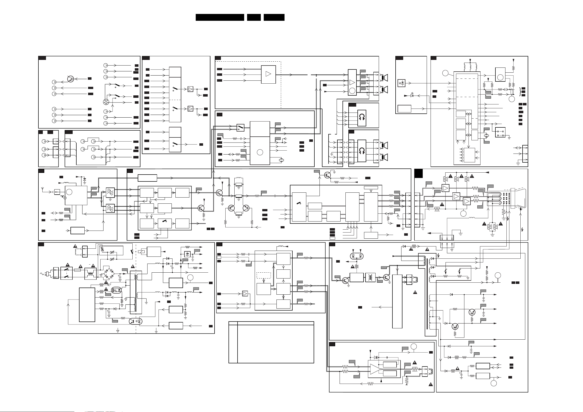
Block Diagram, Testpoints, I2C and Supply Voltage Overview
6. Block Diagram, Testpoints, I2C and Supply Voltage Overview
Block Diagram
27L01.2A 6.
REAR I/O CINCH
A13
MONITOR
OUTPUT
YUV
INPUT
OR
SIDE AV
V
L
R
TUNER IF
A4
V
LOTAUX
FM
SDA
A7
SCL
A7
SEL-IF-LL-M-TRAP
A7
POWER SUPPLY
A1
150 - 250V
SINGLE RANGE
90 - 276V
FULL RANGE
AUDIO/VIDEO
A10
V
L
V-OUT
G-Y-IN
B-U-IN
R-V-IN
MONO
VT
FM
IF
AGC
1
0212
1
2
5500 :
5502
7520
TEA1507
CTRL
CONTROL
A5
A10
A10
A5
A5
A5
STEREO
V
L
R
6001
BZX79-C33
10
11
8
DRAIN
DRIVE R
SENSE
DEMAG
VCC
IC
AV1
R
SVHS
154
V
AV2
L
R
A
B
C
1002
1003
I3
I4
1004
1
R
P
+t
+t
2
+t
6500
AC
6502
3527
3523
6
P2
3525
5
3522
4
3531
1
7101
V
L
R
Y
U
V
E1E
0253
3
0251
3
1
A2
+5V
0265
1
TV
3001
3000
0231
0211
A12
0219
6
3
1
VT_SUPPLY
5001
1000 6, 7 9
2
ERR
10
I1
I2
7001
7002
Degaussing
Coil
MAINS
SWITCH
SC1 L-OUT
SC1 R-OUT
FRONT I/O
V
A
L
B
C
FM-RADIO
TUNER
+
TV TUNER
5
4
FILTER
SELECTION
1
1500
T4E
3
CVBS1-IN
9
STATUS2
11
10
6
Y-CVBS-IN
5
32
4
CVBS-FRONT-IN
L-FRONT-IN
R-FRONT-IN
FM
VIF_1
VIF_2
SIF1
SIF2
RF_AGC
3504
R
3
3
3503
6501
P1
2503
6503
7521
STP7NB60FP
D
G
S
3526
6520
N.C.
2521
3519
P3
HOT GROUND COLD GROUND
A5
A5
L1-IN
A10
R1-IN
A10
A7
A10
C-IN
A5
L2-IN
A10
R2-IN
A10
A10
A10
A10
VIDEO IF, SOUND IF
A5
18
19
22
23
24
A13
A12
2
5520
1
2
3
5
6
7
3
4
SEL_MAIN_FRNT_RR
A12
A13
A13
A12
A13
A13
A12
A5
A13
7209, 7210
FM RADIO
PRE-AMPLIFIER
7200-A
TDA95XX
VIDEO
SOUND
IF + AGC
SOUND
FM-DEMOD.
DE-EMPH.
LF FRONT-IN
1515
43
1
10
9
13
12
1
7515
TCET1103
2
SOURCE SWITCHING
A7
SC2-CTRL
A9
L-FRONT-IN
L1-IN
L2-IN
SC1-LOUT
A9
R-FRONT-IN
R1-IN
R2-IN
SC1-R-OUT
A9
SEL_MAIN_FRNT_RR
A7
CVBS-FRONT-IN
Y-CVBS-IN
IF
AGC
QSS
L1-IN
7580
ENERGIZING
CIRCUIT
7801
HEF4052BT
9
SWITCH
LOGIC
10
1
5
3
2
4
12
14
15
11
FMR
VIDEO
PLL
DEMOD.
QSS MIXER
AM DEMOD.
AUDIO
SWITCH
28 29
V
6562
6564
5562
6560
5560 5563 5561
6561
V
DEFL
7802
HEF4053BT
9
SWITCH
LOGIC
5
2
+13V
LOTAUX
3564
2564
7561, 7562
7564
POWER
DOWN
CIRCUIT
A2
7540, 6540
REFERENCE
CIRCUIT
7541, 7542
STANDBY
CIRCUIT
13
4
VIDEO
AMPLIFIER
SOUND
AMPL.
+ AVL
2561
SY-CVBS-IN
3558
7560
P5
3543
3544
7803
7804
SC1-LIN
SC1 L-OUT
SC1-R IN
SC1 R-OUT
A9
A13
A9
A13
A5
V10
38
+8V
33
48
+3.9V
P4
+3.3V
2567
M_AUX
3570
7
POWER DOWN
P6
MAIN SUPPLY
STDBY_CON
MAIN AUX
95V
AUDIO SUPPLY GND
ERR
7206
3230
MONO/AM_
MONO_SOUND
A8 A9
12V
A8
MONO SETS ONLY
A5
A7
A7
A9
QSS-AM-DEM-OUT
FMR
A11
A5
A10
A10
A7
A7
QSS_AM_DEM_OUT
A6
A2
N.C.
A2
A6
A7
A2
A2
A7
AUDIO AMPLIFIER
7831
MSP34X5G
47
DEMODULATOR
44
41
42
8
7
7203
2254
11
31
S1
34
7941:7943
NICAM, 2CS,
AM, FM
INPUT
SWITCHING
ERR
4
3213
3210
SEL-IF-LL-M-TRAP
7200-D
TDA95XX
VIDEO IDENT
H/V SYNC
SEPARATOR
H-OSC
+PLL
V9
A13
A10
A13
25
24
31
30
4
51
52
2203
C-IN
SY-CVBS-IN
CVBS1-IN
H
V
A10
A9
A8
5241
9
H-DRIVE
2nd LOOP
H-SHIFT
TXT/OSD
DISPLAY
V-DRIVE
GEOMETRY
GEOMETRY
MONO/AM-MONO-SOUND
BASS-PANORAMA
TREBLE-BUZZER-HOSP-APP
NICAM, 2CS BTSC DECODER
7834
7835
MONO/AM-MONO-SOUND
3834 2847
SC1-L IN
SC1-R IN
A7
3833
SDA
SCL
+8V
7201
3208
3211
SYNCHRONISATION
EHT INFO
SANDCASTLE
H FLYBK
POWER-DOWN
EHT INFO
EHT o
A6
3832
AUDIO CARRIER
FILTERS
5201
1200
5.5MHz
1201
6MHz
7202
1202
4.5MHz
3259
3242
7241
3247
ERROR CODE LIST
Error Description
0 No error
1 X-Ray / over voltage protection (USA only)
2 High beam (BCI) protection
3 Vertical guard protection
4 I2C error while communicating with the sound processor
5 Power ON reset (POR bit) 3.3V protection / +8V protection
6 General I2C error
7 Power Down (over current) protection
8 EW protection (Large Screen only)
9 I2C error EEPROM error
10 I2C error PLL tuner
11 Black current loop instability protection
MAIN-OUT-L
MAIN-OUT-L
MAIN-OUT-R
MONO/AM-MONO-SOUND
SC1-L OUT
SC1-R OUT
SC2-CTRL
1831
18M432
7200-C
TDA95XX
40
SWITCHING
VIDEO
45
FILTERS
44
VIDEO
42
IDENT
A7
+8V
30 H DRIVE
17
+
16
EW
15
+
FRONT CONTROL
A12
7901 AN7522N (STEREO)
7902 AN7523N (MONO)
OR
OR
VOLUME MUTE
A7
MAINAUX
62 L+
8
9
ERR
1
7
A12
L+
L+
L-
L-
R-
R-
R+
R+
OR
A10
A10
A5
R-
R+
A10
L+
L-
V4
I/O
Y-DELAY
PAL/NTSC
SECAM
DECODER
7205
3221
47
R-Y
BASE
BAND
B-Y
DELAY
A13
A13
A13
A2
S2
3251
S3
3244
3249
3250
V DRIVE+
V DRIVE-
N.C.
S4
S5
A3
VDRIVE+
VDRIVE-
E1
0254
0246
1
1
2
2
3
3
4
4
5
5
3222
RGB
MATRIX
RGB
INSERT
Y
BLACK
STRETCH
U
WHITE
V
STRETCH
51 52 53 50 54
R-V-IN
G-Y-IN
B-U-IN
FBL-1N.C.
LINE DEFLECTION
V
+13V
LOTAUX
V
A1
DEF
7403
7404
7401
3474
3479
DRIVER
F1
L1
FRAME DEFLECTION
STAGE
WITHOUT
SIDE AV
+HP
A1
0246
4
A2
A3
A4
R
G
B
M_AUX
HFLYBK
L+
L-
R-
R+
A13
CONTROL
OSD TEXT
INSERT
BLUE
STRETCH
WHITE-P.
7204
EHT INFO
PROC.
6406
BAV70
5444
OSD
RGB
ADJ
3
2
1
0255
4
3
2
1
4L-
10 R-
12 R+
HEADPHONE
HEADPHONE
V-OUT
+8V
3404
A6
VLOT AUX +13V
6471
2
7471
TDA9302H
7
+
OP. AMP
1
-
F2
3475
56
R
57
G
B
58
55
MAIN SUPPLY
L3
7402
BUT11APX
L2
2473
6
FLYBACK
GENERATOR
THERMAL
PROTECTION
4
-13V
95V
L
R
L
R
3201
3202
3203
3204
3235
6692
TSOP1836
+3.3V
V5
V6
V7
V9
BLK
BLK-IN
A2
EHT INFO
LINE
OUTPUT
CIRCUIT
LOCAL
KEYBOARD
0243 0245
A2
6409
F5
3
F3
5
F4
1
2
3
4
5
6
0221
1
2
IR IR
6691
LED
KEYBOARDPROTN
B
1
2
3
4
5
6
+160V
3416
VIDEOSUPPLY
2
7
1
HOR.
DEFL.
COIL
ERR
3
V_GUARD
3471
3471
CRT
V11
V13
BLKCURINFO
5445
0222
1
2
VERT.
DEFL.
COIL
CONTROL
A7
STATUS1
STATUS2
A13
A1
POWER DOWN
KEYBOARD-
7311:
7313
V12
3347
0244
0220
8
5
4
N.C.
3
10
9
6
A2
ERR
5
N.C.
LED
_PROTN
3316 3326
-
7321:
7323
FILAMENT
321
EHT
FOCUS VG2
6402
6410
6405
6423
3411
6413
67
1
69
5
80
-
3421
7408
7200-B
TDA95XX
TRANSCEIVER
ROM
RAM
1/10
PAGES
MEMORY
TELE
TEXT
SYNC
CVBS
R
G
B
BL
COR
3317
7331:
7333
3423
3428 3427
+3.3V
66 61 59
I/O
IIC
BUS
I/O
PORTS
OSD
TELETEXT
DISPLAY
-
ERR
11
2417
2419
3336
R
5341
7407
L7
3413
3412
56035602
PWM-
G
B
VST
DAC
CPU
3317
3327
3337
3422
L8
7406, 7409
7405
5604
68 7
72
71
3
6
70
78
77
73
63
64
H
V
V15
V16
3349
V
LOTAUX
L4
L5
L6
PROT
CIRCUIT
PROT
CIRCUIT
+3.9V
C4
C5
C1
12MHz
C2
V14
7
5
3
3425
3431
2422
2410
+3.3V
7602
M24C08
EEPROM
8
(NVM)
6
ERR
5
9
36063607
3625
SDA
3624
SCL
ERR
6
SEL-IF-LL-M-TRAP
STANDBY-CON
SEL-MAIN-FRONT-RR
BASS PANORAMA
TREBLE-BUZZER-HOSP-APP
VOLUME/MUTE
SDM
9641
9631
1660
CONNECTION
SDA
SCL
+160V
R
G
B
3348
3350
G2
V FOCUS
V
+13V
ERR
2
EHT INFO
A5 A6
V
+13V
LOTAUX
V
+5V
LOTAUX
+8V
FILAMENT
-13V
VT_SUPPLY
A4
V
A3
GUARD
BLK-IN
A5
EHT o
A6
ERR
2
CL 16532052_001.eps
3611
36033604
SDA
SCL
A4 A5
A1
A10
A8
A8
A8
SERVICE
COMPAIR
CRT
230801
EHT
A4
A7
A9
0217
25kV
1
2
3
Page 48

Block Diagram, Testpoints, I2C and Supply Voltage Overview
Testpoint Overview
Main Panel
Copper Track Side
NICAM + 2CS + BTSC
7831
CRT Panel Copper Track Side
5
4
3
2
12
11
6
7
8
9
10
5
6
7
8
9
HOT GROUND
HOT GROUND
AUDIO OUTPUT
7901 OR 7902
14
7520
85
SUPPLY
CONTROL
1
7521
D
SUPPLY
A1
A2
A3 - A4
S
G
2V / div DC
5us / div
2V / div DC
500us / div
2V / div DC
500us / div
7200
A6
2V / div DC
200us / div
A7
2V / div DC
200us / div
A11
1V / div DC
500us / div
TV-PROC.
7402
C
C1
C2
C4
28L01.2A 6.
E
LINE
B
1V / div DC
500us / div
1V / div DC
500us / div
2V / div DC
200us / div
C5
2V / div DC
200us / div
F1
500mV / div DC
5ms / div
F2
500mV / div DC
5ms / div
7471
7
1
FRAME
F3
10V / div DC
5ms / div
F4
1V / div DC
5ms / div
F5
10V / div DC
5ms / div
A1 B3
A2 B3
A3 A3
A4 A3
A5 C1
A6 B1
A7 B1
A8 C2
A9 B2
A10 B3
A11 C2
A12 B2
A13 C3
C1 B4
C2 B4
C3 B5
C4 B5
C5 B5
C6 E1
F1 D6
F2 D6
F3 C6
F4 C6
I1 A6
I2 A6
I3 A6
I4 A6
L1 C4
L2 E5
L3 E5
L4 D5
L6 C5
L8 C6
L9 D5
P1 E3
P2 E3
P3 D3
P4 C4
P5 C4
P6 D5
S1 A4
S2 A4
S3 A5
S4 A5
S5 A4
V1 B6
V2 B6
V3 B5
V4 B4
V5 B4
V6 B4
V7 B4
V8 B4
V9 A4
V10 A4
I1
2V / div DC
200us / div
I2
2V / div DC
200us / div
I3
20mV / div DC
1ms / div
I4
500mV / div DC
250ns / div
L1
500mV / div DC
20us / div
L2
2V / div DC
20us / div
L4 = +13V
L5 = +5V
L6 = +8V
L7 = -13V
L8 = +34V
L10 = +176V
L9
2V / div DC
20us / div
P1
50V / div DC
20us / div
P3
5V / div DC
50ms / div
P2 = +308V (317V)
P4 = +3V3
P5 = +12V4 (+3V9)
P6 = +95V
S1
2V / div DC
20us / div
S2
500mV / div DC
20us / div
S3
500mV / div DC
5ms / div
S4
500mV / div DC
5ms / div
V4
100mV / div DC
20us / div
V5
1V / div DC
20us / div
V6
1V / div DC
20us / div
V7
1V / div DC
20us / div
V8
2V / div DC
5ms / div
V9
500mV / div DC
10us / div
V10
1V / div DC
500us / div
V11
1V / div DC
20us / div
V12
1V / div DC
20us / div
V13
1V / div DC
20us / div
V14
50V / div DC
20us / div
V15
50V / div DC
20us / div
V16
50V / div DC
20us / div
CL 16532008_033.eps
240801
Page 49

Block Diagram, Testpoints, I2C and Supply Voltage Overview
I2C and Supply Voltage Diagram
POWER SUPPLY
A1
0231
0211
150 - 250V
SINGLE RANGE
90 - 276V
FULL RANGE
MAINS
SWITCH
I2C BUS INTERCONNECTION DIAGRAM
CONTROL
A7
7200-B
SET
ERR
72
71
68
5
PROCESSOR
PART OF
VIDEO-
PROCESSOR
ERROR CODE LIST
Error Description
0 No error
1 X-Ray / over voltage protection
2 High beam (BCI) protection
3 Vertical guard protection
4 I2C error while communicating with the sound processor
5 Power ON reset (POR bit) 3.3V protection / +8V protection
6 General I2C error
7 Power Good (over current) protection
8 EW protection (Large Screen only)
9 I2C error EEPROM error
10 I2C error PLL tuner
11 Black current loop instability protection
C4
SDA
SCL
C5
+3.9V
3607 3606
+3.9V
1500
T4E
3
5500 :
5502
7520
TEA1507
CTRL
CONTROL
3625
3624
7
DRAIN
DRIVE R
DEMAG
IC
3604
M24C08
EEPROM
SENSE
VCC
7602
(NVM)
ERR
29L01.2A 6.
B
6560
6561
5560 5563
6500
6501
AC
6502
6503
3527
8
3523
6
3525
5
3522
4
3531
1
3603
65
9
7521
STP7NB60FP
G
P2
2521
ERR
6
0217
1
2
3
P1
5520
1
2503
2
3
D
S
5
3526
6520
P3
SDA
SCL
FOR
COMPAIR
6
7
N.C.
3519
3
4
HOT GROUND COLD GROUND
TUNER IF
A4
I1 I2
3001
1000
TUNER
ERR
10
13
12
10
9
1
7515
TCET1103
2
3000
45
SDA
SCL
5562
7540, 6540
REFERENCE
CIRCUIT
7541, 7542
STANDBY
CIRCUIT
NICAM, 2CS,
A9
BTSC DECODER
3833
A7 A8
7831
MSP34X5G
SOUND
DECODER
ERR
4
6564
6562
3549
3832
78
2561
3564
2564
7561, 7562
7564
POWER
DOWN
CIRCUIT
A
3543
3544
P6
5561
A
P5
3537
AUDIO SUPPLY GND
7560
3557
3558
STDBY_CON
SDA
SCL
MAIN SUPPLY
12V
M_AUX
MAIN AUX
POWER DOWN
V DEFL.
P4
2567
A7
95V
+3.3V
+3.9V
CONTROL
A7
+3.3V
+3.9V
(TO 3606
3606,3633)
SYNCHRONISATION
A6
+3.3V (TO 3256)
FRONT CONTROL
A12
+3.3V
4693
A8
MAIN AUX
AUDIO SUPPLY
GND
+3.3V
5602
5603
5604
3611
+3V3A
AUDIO AMPL.
OR
OR
7200-B
66
61
uC
59
7602
8
EEPROM
(NVM)
7901
1
OUTPUT
STEREO
7902
1
OUTPUT
AUDIO
AUDIO
MONO
V DEF
LINE DEFLECTIONA2
MAIN SUPPLY
M_AUX
VLOT AUX +13V
6467
H-DRIVE
3487
2450
3404
LINE
OUTPUT
5451
6406
5445
EHT
FOCUS
LOT
2
VG2
6409
73
9
6405
6
6410
8
6402
5
VLOT AUX +5V
NICAM 2CS -
A9
BTSC DECODER
VLOT AUX +5V
5833
AUDIO VIDEO
A10
SOURCE SWITCHING
+8V
3801
REAR I/O CINCH
A13
+8V (TO 7101-C)
7408
34243423
+8V
+5VA
34116413
34286423
3421
5832
to 2419
7407
+8V
SUPPLY
FILAMENT
3412
3413
6420
TO E-7406
46
33
VIDEO
3416
0220
2
1
-13V
3427
VT_SUPPLY
VLOT AUX +5V
C-6408
B-7409
3422
6419
+8V
VLOT AUX +5V
VLOT AUX +13V
3415
7831
BTSC
DECODER
+6V8
TO
CRT
EHT
ANODE CRT
FOCUS
FOCUS CRT
VG2
VG2 CRT
0244
160V
3
5341
2
1
TUNER IF
A4
VT_SUPPLY 33V
VLOT AUX +5V
FRAME DEFLECTION
A3
VLOT AUX +13V
POWER SUPPLY
A1
VIDEO IF
A5
SYNCHRONISATION
A6
+8V
CONTROL
A7
AUDIO AMPLIFIER
A8
3349
3350
6001
BZX79
-/C33
5001
+8V (TO 3008)
-13V
VLOT AUX
VLOT AUX +13V
TO DEGAUSSING CIRCUIT
VLOT AUX +5V
(TO 2234)
+8V
5202
+8VA (TO 3248)
5241
+8V (TO 4-0217) NOT USED
VLOT AUX
+8V (TO 3948, 3950)
VLOT AUX
3336
3326
3316
+8VA
+5V (TO 3619)
+5V (TO 9921)
CL 16532052_002.eps
VIDEO
OUTPUTS
C-7332
C-7322
C-7312
TO CRT
FILAMENT
1000
9
TUNER
6
7
7471
4
FRAME
OUTPUT
3
7200-A
VIDEO
39
7200-D
SYNC
9
PROC.
IF
230801
Page 50

7. Schematics and PWB’s
Large Signal Panel: Power Supply
Schematics and PWB’s
30L01.2A 7.
123456789101112
POWER SUPPLY
P3
F501
F502
I528
9500
*
0231
*
SDKV
56
24
13
MAINS SWITCH
I501
*
3500
I502
3501
3531
I531
0R
2528
6520
BYD33D
I507
*
3521
5V / div DC
50ms / div
F503
9501
3M3
3M3
RES
6522
*
2505
I509
F504
F506
(13V8)
RES
F505
16V8
1V3
3520
P4 = +3V3
P5 = +12V4 (+3V9)
P6 = +95V
2n2
1500
T4E.250V
7520
TEA1507
1
Vcc
2
Gnd
INPUT
CONTROL
3
Ctrl
CIRCUIT
BURST
DETECTOR
POWER SUPPLY
ITEM
NO
1K2
100n
2520
0213
0231
1515
2503
2504
2505
2516
2580
3502
3503
3504
3505
3508
3521
3523
3526
3544
3545
3563
3580
5500
5501
5502
5520
5562
6561
6567
6570
6580
6581
7521
7580
9500
9501
9502
9503
9520
I529
2500
SUPPLY
MANAGEMENT
FREQUENCY
CONTROL
FR20/21
AP
---
2P 8/128A SDKV
---
220u/400
---
2n2
---
---
NTC 4R7
---
PTC/PTC 9R/100R
---
--4R7
47R
0R15
6K8
82K
8K2
---
DMF2820H
---
---
S359B4-09
100MHZ 80R
BYW76
BZX384-C4V7
BZX384-C6V2
---
---
7NC80ZFP
---
---
---
---
JUMPER
---
470n
3506
220R
I547
VOLTAGE
CONTRLLED
OSCILLATOR
TEMPERATURE
PROTECTIOM
POWER-ON
F524
3
+t
Rs
3503
3504
Rp
*
1
*
2
3508
*
1M5
1
5500
4
*
3505
3
*
V
4
3
*
3507
DMF-2820
2
1
2
6
*
5501
5502314
C914
DSP
VALLEY
OVER
RESET
2P 8/128A SDKV
PTC/PTC 9R/100R
BZX384-C4V7
BZX384-C6V2
LOGIC
CONTROL
CIRCUIT
MAXIMUM
ON-TIME
PROTECTION
DIVERSITY TABLE FOR ALL ITEM NO. MARKED WITH
HR14
AP
---
---
100u/400
--2n2
330p
---
NTC 4R7
---
---
---
22R
100R
0R18
6K8
82K
8K2
---
---
DMF2430H22
--SS28010-06
100MHZ 50R
---
---
---
4NC80ZFP
---
---
---
JUMPER
JUMPER
---
HR
15RF/20/21
AP
---
2P 8/128A SDKV
---
100u/400
--2n2
330p
---
NTC 4R7
---
PTC/PTC 9R/100R
---
--4R7
47R
0R15
6K8
82K
8K2
---
DMF2820H
---
---
S359B4-09
100MHZ 80R
BYW76
BZX384-C4V7
BZX384-C6V2
---
---
6NC80ZFP
---
---
---
---
JUMPER
---
+t
10R - PTC
9502
*
3502
*
t
0213
*
2
1
START-UP
CURRENT SOURCE
START-UP
CURRENT SOURCE
CURRENT
SENSING
OUTPUT
DRIVER
OVER
POWER
PROTECTION
FR14
AP
---
2P 8/128A SDKV
---
200u/400
--2n2
330p
---
NTC 4R7
---
PTC/PTC 9R/100R
---
---
22R
100R
0R18
6K8
82K
8K2
---
DMF2820H
---
---
SS28010-06
100MHZ 50R
--BZX384-C4V7
BZX384-C6V2
---
---
6NC80ZFP
---
---
---
---
JUMPER
---
2n2
2501
2n2
2502
For ITV
ONLY
Drain
HVS
Demag
Sense
Driver
*
FR
15RF/20/21
AP
---
2P 8/128A SDKV
---
200u/400
---
2n2
330p
---
NTC 4R7
---
PTC/PTC 9R/100R
---
--4R7
47R
0R15
6K8
82K
8K2
---
DMF2820H
---
---
S359B4-09
100MHZ 80R
BYW76
BZX384-C4V7
BZX384-C6V2
---
---
7NC80ZFP
---
---
---
---
JUMPER
---
1N5062 (COL)
1N5062 (COL)
"$"
8
7
0V
4
5
0V
6
2V
I503
6500
1N5062 (COL)
6502
1N5062 (COL)
I504
47K
3529
I546
4K7
3530
I508
3522
330K
I510
3525
1K
HR
20/21
CH
---
2P 8/128A SDKV
---
100u/450
--2n2
330p
---
NTC 4R7
---
PTC/PTC 9R/100R
VDR 1MA/423V
--4R7
47R
0R15
6K8
82K
8K2
---
DMF2820H
---
---
S359B4-09
100MHZ 80R
BYW76
BZX384-C4V7
BZX384-C6V2
---
---
6NC80ZFP
---
---
---
---
JUMPER
---
6501
6503
6523
1N4148
0V2
7522
BC847B
2522
100n
I511
3524
56K
SOUND AMPLIFIER
ITEM
NO.
2566
3560
3564
3567
3568
3570
7562
7564
P1
F510
F507
2n2
*
2503
2506
2504
*
3527
I506
2K2
1V5
1V5
I533
I512
3523
I532
2525
SNDAMP
1X4W-MN-CH
47uF/25V 47uF/25V -
47R 47R 0R1
2K2 2K2 8K2 8K2 -
-BC857B
BC857B BC857B
F514
F508
P2
*
I514
"$"
7521
*
D
S
G
0V
3528
10K
2524
RES
1n
*
3526
2526
*
470p
DIVERSITY TABLE FOR ALL ITEM NO. MARKED WITH
SNDAMP
2X3WST-NA/LA/AP
0R1 4R7
BC857B -
*
"$"
2n2
RES
2507
2508
9520
5521
1n5
2523
2527
RES
6521
3519
270R
TCET1103(G)
2X1W-ST-GL
1515
*
G5P
9503
23
2516
*
EAR
5520
*
1
470p
I536
3
F509
5
6
78
470p
I513
8V9
3
7515
42
10V
SNDAMP
-
-
*
6581
14
I530
7580
*
BC857B
330p
2515
I544
5562
*
1n5
2569
132
12
11
10
9
5560
I538
2565
470p
1V3
1
3540
I515
16V4
3546
I516
5K6
3569
7542
BC857B
6V2
I523
7V
3566
*
6570
2K2
2568
1u
*
SNDAMP
1X4W-MN-LA/AP
47uF/25V 47uF/25V
47R
0R1 0R1
2K2 2K2
8K2 8K2
BC857B
BC857B BC857B
SNDAMP
1X3W-MN-GL
47R
-BC857B
6580
I520
EGP20DL
3561
470p
I545
6563
I522
I539
RES
3541
470R
0R
PDTC114ET
9V
7V
I548
I549
VlotAux+13V
*
*
F525
2562
1n
6562
6564
SB340
220R
*
BZX384-C4V7
BAS216
2560
1n
6560
BYW76
6561
*
BYW76
I526
6541
7541
2541
1n
3552
10K
6569
BAS216
47K
3580
*
F512
6567
2563
100n
3562
10K
I541
BZX79-C10
I517
0V
F517
2564
3542
6540
3565
330R
2580
47u
I535
*
I521
2m2
*
3567
5563
I527
1K5
8V3
6V
BZX79
3560
2K2
-2V9
4500
F526
7540
BC547B
B6V2
*
47R
4V8
F513
3548
8K2
2542
RES
3558
3564
0R1
7564
*
BC857B
2566
*
47u
7562
*
BC857B
3563
*
I540
2561
6V3
3547
0R33
6566
BAS216
5505
3559
330R
11V6
to 0303 of
+3.3V
-V28
92V4
(95V)
47u
F515
F516
I518
2540
3545
CN:
1K
13V
I534
0302
15n
*
I537
SVT2004
12V
3568
I519
*
I525
7560
LE33CZ
13
3V3
2
F519
12V7
P5
*
3V3
7561
PDTC143ZT
5561
27u
3549
220R
82K
3543
6K8
3544
F522
2567
F521
F520
3550
F523
F518
9504
2559
RES
I543
47u
F511
3570
*
RES
+3.9V
(3V9)
6565
BAV70
P4
+3.3V
(3V3)
M_Aux
12V4
(3V9)
TO
AudioSupplyGnd
10R
MainAux
POWER_DOWN
MainSupply
(95V)
P6
Vdef
0251
1
2
3
4
FOR ITV ONLY
0282
MainSupplyGnd
Stdby_con
OF
A7-11
A2-64
TO
0251
OF
TO 0283
OF
OFTO
A7-5
CL 16532101_025.eps
A
B
C
D
E
F
G
H
230801
A
B
C
D
E
F
G
H
P1 P2 = +308V (317V)
50V / div DC
20us / div
DEGAUSSING COIL
0212
0211
MAINS
150 - 276 V SINGLE RANGE
90 - 276 V FULL RANGE
P3
2521
"$"
FOR MAINS 120V AC 170V (177V)
..V.. Normal Operation
(..V..) Standy Mode
HOT GROUND
COLD GROUND
1
2
2
1
I505
22u
220V AC 309V (317V)
0211 C2
0212 B2
0213 C5
0231 C2
0251 E11
0282 F12
0302 D10
1500 C3
1515 A8
2500 C4
2501 B5
2502 C5
2503 C7
2504 C7
2505 B3
2506 C7
2507 C7
2508 C8
2515 C8
2516 B8
2520 G3
2521 E2
2522 D7
2523 D7
2524 D7
2525 F7
2526 E7
2527 D8
2528 E2
2540 F10
2541 G9
2542 F10
2559 G11
2560 E9
2561 E10
2562 C9
2563 D9
2564 C9
2565 E8
2566 C10
2567 B11
2568 G9
2569 C9
2580 B9
3500 D2
3501 D2
3502 C5
3503 B5
3504 B5
3505 C5
3506 D4
3507 D4
3508 B5
3519 E8
3520 G3
3521 F2
3522 D6
3523 E7
3524 E7
3525 E6
3526 E7
3527 C7
3528 D7
3529 C6
3530 D6
3531 E2
3540 F9
3541 F9
3542 F9
3543 F10
3544 F10
3545 F10
3546 F9
3547 F10
3548 E10
3549 E11
3550 F11
3552 G9
3558 B10
3559 B10
3560 C10
3561 C9
3562 D9
3563 D10
3564 C10
3565 A10
3566 G9
3567 C10
3568 C10
3569 F8
3570 D11
3580 B9
4500 D10
5500 C4
5501 C4
5502 D4
5505 G10
5520 C8
5521 D7
5560 E9
5561 E11
5562 C9
5563 E10
6500 B6
6501 B6
6502 B6
6503 B6
6520 F2
6521 E7
6522 E3
6523 C6
6540 F9
6541 F9
6560 E9
6561 E9
6562 C9
6563 D9
6564 C9
6565 B11
6566 G10
6567 D9
6569 G9
6570 G8
6580 B9
6581 B9
7515 F8
7520 D3
7521 D7
7522 D6
7540 F10
7541 F9
7542 G8
7560 B11
7561 D10
7562 C10
7564 C10
7580 B8
9500 C2
9501 C3
9502 C5
9503 B8
9504 D11
9520 D7
F501 B2
F502 B2
F503 C3
F504 C3
F505 C3
F506 C3
F507 B7
F508 C7
F509 D8
F510 B7
F511 C11
F512 C9
F513 E10
F514 C7
F515 E10
F516 E10
F517 G9
F518 B11
F519 B11
F520 E11
F521 D11
F522 F11
F523 F11
F524 A5
F525 B9
F526 D10
I501 C2
I502 D2
I503 B6
I504 C6
I505 E2
I506 C7
I507 F2
I508 D6
I509 F3
I510 D6
I511 E6
I512 E7
I513 E8
I514 D7
I515 F9
I516 F9
I517 F9
I518 E10
I519 F10
I520 C9
I521 C10
I522 D9
I523 G8
I525 A11
I526 E9
I527 E10
I528 C2
I529 C4
I530 B8
I531 E2
I532 F7
I533 D7
I534 C10
I535 C10
I536 C8
I537 F10
I538 E8
I539 E9
I540 E10
I541 E9
I543 A11
I544 C8
I545 D9
I546 C6
I547 D4
I548 G9
I549 G9
123
456789101112
Page 51

Schematics and PWB’s
Large Signal Panel: Line Deflection
31L01.2A 7.
A
B
C
D
E
G
H
123456789101112
LINE DEFLECTION
L9 L4 = +13V
2V / div DC
20us / div
F410
6406
BAV70
11V6
*
L1
15n
18K
27u - 33u
02475
3404
I444
6R8
5V4
10K
3406
7403
BC337
5V4
I446
7404
BC636
5V4
7401
PDTC143ZT
---
-
-
--
-
---
-
--
-YY
Y
21" Mec
680p 680p
430p
13n
18K
220R 220R
1K 1K
3K3
56801
02466
BAV21 BAV21
Y
L5 = +5V
L6 = +8V
L7 = -13V
L8 = +34V
L10 = +176V
I404
11V
L9
*
2405
5V4
5V6
I445
0V
2403
2406
*
1V4
F409
21" China
-
-
-
-
--
-
--
--
--
-
470p
-
330p
12n
-
-
330K
18K
39K
10K
-
3K3
94864
02466
Y
3407
9404
*
2411
47u
*
VlotAux+5V
6408
*
I402
*
5401
BAS316
I405
5406
I403
2415
*
I406
*
I408
3
1n
1
2401
*
9405
6401
*
6403
*
9403
5403
*
3401
*
3402
*
for sets
w/o quasi
diode
modulation
5444
SC10009-03
3429
*
*
6416
F405
6
L2
F401
*
2402
I401
2K2
3405
7402
BUT11APX
F406
3432
I407
for sets
with quasi
modulation
F402
0V
3430
*
2400
*
diode
2404
22R
*
F403
F404
90V8
0V
F407
4
1
0221
VH
L3
6404
2408
6412
*
*
BYD33M
*
*
F408
9401
5410
9408
5408
I424
2407
9402
27u
*
*
2424
HORIZONTAL
DEFLECTION
COIL
I425
3403
*
*
2416
*
2409
47u
I447
VideoSupply
I432
10
FILAMENT
6409
BYD33D
5445
*
1
7
2
6
9
3
4
5
0220
1
2
3
2413
I433
I431
10u
3416
I434
EHT
8
TO 0224 OF
CRT PANEL
VideoSupply
L10
3R9
TO PICTURE TUBE
TO CRT
VFOC
PANEL
VG2
3418
F414
2412
1N4148
33K
I450
33n
6413
I449
6415
I413
BAS216
2420
VlotAux+5V
I414
I440
3411
10R
3413
10K
1u
3419
12V5
6417
6402
BYD33D
6410
BYD33D
7408
BD135
I415
VlotAux+13V
6R8
BZX284-C10
I411
F415
8V4
6405
BYD33D
6423
BYD33D
12V4
I456
I451
BC857B
7406
7409
BC857B
*
3431
I430
*
3425
12V4
2410
F419
2414
BZX79-C5V6
8V
8V7
5V5
470u
1m
3424
100R
3428
39R
3421
6R8
6419
F417
2419
5V
8V5
I457
F412
I459
1u
BD135
I452
3412
*
3414
BZX79-B6V2
I412
I454
4V5
3420
7407
5V
5V7
3422
100R
I455
3423
820R
6420
BZX79-C9V1
2417
1m
3427
27K
2423
10u
BC857B
7405
4V5
*
6414
33K
2418
10n
6V2
I435
I453
2V1
3415
1K
3426
1M
2421
47n
3417
33K
F418
3410
33K
EHTo
VlotAux+13V
BLK-IN
Vguard
EHTinfo
A6-23
A5-36
A3-65
A5-16
A6-16
A
B
C
L4
F411
F416
2422
F413
L5
470u
L6
L7
L8
VlotAux+13V
VlotAux+5V
+8V
VlotAux+13V
VlotAux-13V
VT_Supply
D
E
F
G
H
CL 16532101_026.eps
230801
11 12
M_Aux
Hdrive
Hflybk
Vdef
+95V
I448
L2
2V / div DC
20us / div
12V4
12V
6407
BAS216
3408
L1
500mV / div DC
20us / div
MainSupply
A1-64
VlotAux+13V
A6-21
A6-18
F
ITEM
14" CPTO
2400 - 2401 680p
2402 -
430p 360p
2404
2405
2406 330p
2407
2408
2416
2424
3401
3403
3407
3408
3412
3414
3425
3429
5401
5403
5406 - 56801
5408
5445
6401 BAV21 BAV21 BAV21
6412 6416
9402
9403
9404
9408
--
---
820p
---
330K
18K3402
-
220R
1K
39K
12K
15K
-
-3430
2K23431
--
- 27u
-
02475
----YYYYY
YYY
Asia Pacific/China
15" RF SMGK 20" CPTO
680p 680p
- 680p
330p 330p 330p
12n11n
820p 390p 820p 2n2
330K 330K 330K
18K
--
220R 220R
1K 1K
39K 39K 39K
12K 12K 12K 12K
12K 15K 10K
-
2K7 0R
02475
----
Y
12345678910
0220 F7
0221 B5
2400 F5
2401 A4
2402 B5
2403 E3
2404 B5
2405 D3
2406 E3
2407 D6
2408 B6
2409 C6
2410 D9
2411 D4
2412 C8
2413 A7
2414 E9
2415 D4
2416 D6
2417 F10
2418 B11
2419 B10
2420 B9
2421 B11
2422 E11
2423 F10
2424 E6
3401 C5
3402 C4
3403 B6
3404 D3
3405 C5
3406 D3
3407 B4
3408 D2
3410 B11
3411 A9
3412 A10
3413 A9
3414 A10
3415 A11
3416 A8
3417 B11
3418 B8
3419 B9
3420 B10
3421 D10
3422 E10
3423 E10
3424 E10
3425 C10
3426 B11
3427 F10
3428 F10
3429 F5
3430 F5
3431 C10
3432 D5
5401 C4
5403 B4
5406 C4
5408 B6
5410 F6
5444 D4
5445 B7
6401 B4
6402 D9
6403 B4
6404 D6
6405 F9
6406 C2
6407 D2
6408 F4
6409 B7
6410 D9
6412 E6
6413 A9
6414 A11
6415 B9
6416 F4
6417 B9
6419 E10
6420 E10
6423 F9
7401 E3
7402 D5
7403 D3
7404 D3
7405 A11
7406 B10
7407 D10
7408 E9
7409 B10
9401 F6
9402 E6
9403 B4
9404 C4
9405 B4
9408 B6
F401 B5
F402 B5
F403 B5
F404 B5
F405 D5
F406 D5
F407 E5
F408 E6
F409 E3
F410 B3
F411 D11
F412 F10
F413 E11
F414 C8
F415 D9
F416 D11
F417 A10
F418 B11
F419 D10
I401 B5
I402 B4
I403 D4
I404 D3
I405 B4
I406 C4
I407 F5
I408 C4
I411 D9
I412 B10
I413 A9
I414 C9
I415 F9
I424 B6
I425 B6
I430 C9
I431 A8
I432 B7
I433 B7
I434 B7
I435 B11
I440 D9
I444 D3
I445 D3
I446 D3
I447 D7
I448 D2
I449 A9
I450 B9
I451 F9
I452 A10
I453 A11
I454 B10
I455 E10
I456 F9
I457 E10
I459 F10
Page 52

Schematics and PWB’s
Large Signal Panel: Frame Deflection
32L01.2A 7.
A
B
C
D
E
123456789101112
FRAME DEFLECTION
A
B
Vguard
A2-65
VlotAux+13V
Vdrive+
A6-19
Vdrive-
A6-20
F477
F478
3473
3475
3474
1K
2K2
3479
1K
2K2
F471
I472
2477
470p
2475
470p
I473
VlotAux-13V
F5
6471
2473
BYD33D
12V5
7471
TDA9302H
2471
100n
F1
0V9
F2
F472
VSUP6VSUPO
7
IN+
POWER
AMPLIFIER
1
IN-
F479
2
GND
2472
4
-13V4
I477
12V8
100n
100u
-12V2
3
FLYB
FLYBACK
GENERATOR
THERMAL
PROTECTION
2476
220n
OUT
6472
6473
BYD33D
F473
3477
BYD33D
I476
3478
220R
220R
F474
F3
0222
1
2
F4
VERTICAL
DEFLECTION
COIL
9471
0V
5
I474
3476
I475
5471
Bead
1R5
C
D
E
0222 D8
2471 C5
2472 E6
2473 C6
2475 D4
2476 D6
2477 D4
3471 F7
3472 F8
3473 D4
3474 C4
3475 E4
3476 D7
3477 D7
3478 E7
3479 D4
5471 D7
6471 C6
6472 D7
6473 D7
7471 C5
9471 D7
F471 C5
F472 E5
F473 D8
F474 D8
F475 E7
F476 E8
F477 C3
F478 D3
F479 E6
I472 C4
I473 D4
I474 D7
I475 E7
I476 E7
I477 C6
F
G
H
ITEM
14" CPTO 15" RF SMGK 20" CPTO
3471 5R6 3R3 3R3 3R3 3R3
3472 5R6
F1
500mV / div DC
5ms / div
Asia Pacific/China
21" Mec 21" China
3R9 5R6 3R3 3R9
F2
500mV / div DC
5ms / div
F3
10V / div DC
5ms / div
F4
1V / div DC
5ms / div
F5
10V / div DC
5ms / div
F475
3471
3472
F476
CL 16532101_027.eps
230801
F
G
H
123456789101112
Page 53

Large Signal Panel: Tuner IF
Schematics and PWB’s
33L01.2A 7.
G
A
B
C
D
E
F
123456789101112
TUNER IF
I1
2V / div DC
200us / div
Diversity Table
BGIDKM
ITEM
1002
1003
1004
2003
3006
3007
3008
4001
4002
4003
4004
4012
5003
6004
7001
PDTC124ET
LA/NA/AP
INDIA/AP QSS-AP
072TPL-A
K7260M
---
--10n
2K2
6K8
2K2
---
---
---
Jmp
---
---
BA792
I2
M-MN
---
---
---
---
---
--Jmp
Jmp
---
---
---
---
---
---
2V / div DC
200us / div
BGIDKM
K7257M
K9362M
PDTC124ET
---
10n
2K2
6K8
2K2
---
--Jmp
Jmp
Jmp
1n8
BA792
TO 0282
I3
20mV / div DC
1ms / div
FOR ITV ONLY
0285
FOR EMC ONLY
OF
0283
SCL RF_AGC
A7-13
SDA
A7-14
A5-24
SEL-IF-LL_M-TRAP
A7-3
BGDK
AP
K2960M
---
---
---
---
---
--Jmp
Jmp
---
---
---
---
---
---
FM
I4
500mV / div DC
250ns / div
F007
F008
F009
F005
1000
*
12
13
14
15
3000
100R
3001
100R
3010
100R
TUNER
MT
AS SCL SDA
345678
I001
I002
4.3V
I2
*
2001
2002
3011
+5V ADC
4.3V
I1
*
RES
FM-RADIO ANTENNA
F010
AGC
FM-ANT
+5V
VT
FM
IF
4.9V
10
11
0265
2010
1
2
9
5V
1
33V8
F003
I005
Diversity Table
ITEM
Stereo Mono
UR1316R
*
I010
3005
100R
4002
4012
1000
2001
22p
22p
2002
3010
330R
3011
5002
22n
2009
1002
*
1
2
3
1003
*
10
1
2
*
1
2
SWI
IN
ING
1004
GND
3
O1
O2
8
3
I006
I007
RES
4005
7002
RES
6002
6003
3002
6005
RES
RES
JMP
VlotAux+5V
5001
2006
3009
*
5u6
470u
RES
*
2007
9001
4003
I018
100n
I011
3003
1K5
3004
I008
*
4004
4011
RES
8K2
I009
VT_Supply
2
3
1n
F001
F002
I4
F004
I3
*
2003
3006
*
5V
7001
*
0V
2004
5002
I003
*
*
2005
47n
4001
RES
4006
3007
6004
10u
6001
BZX79-C33
I016
100u
2008
+8V
**
3008
*
*
FM Radio
UR1316R UV1356A
---
---
F006
4
5
4
5
4
5
AP/CH 38.9/38.0
LNA
22p
22p
Jmp
330R
5003
---
---
---
---
---
820n
I013
2u7
I014
Non-LNA &
Non FM Radio
TEDE9-228A
22p
22p
---
---
820n
LA/NA/AP 45.75
Non-LNA
LNA
UV1336A ENV56D98G3
TEDH9-200A
VIF_1
VIF_2
SIF_1
SIF_2
---
---
---
---
820n
A5-25
A5-27
A5-26
A5-28
A5-29
---
---
---
---
820n
A
B
C
D
E
F
G
0265 A5
0283 C3
0285 B3
1000 B4
1002 D8
1003 E8
1004 F8
2001 D4
2002 D5
2003 D6
2004 B6
2005 B6
2006 B7
2007 B7
2008 C6
2009 C9
2010 B5
3000 C4
3001 C4
3002 C7
3003 B8
3004 C8
3005 C8
3006 E6
3007 D6
3008 D6
3009 D7
3010 D4
3011 D5
4001 D6
4002 F8
4003 E7
4004 E8
4005 E7
4006 E6
4011 F8
4012 G8
5001 B7
5002 C6
5003 F9
6001 B6
6002 C7
6003 C7
6004 E6
6005 E7
7001 F6
7002 F7
9001 D7
F001 B6
F002 B6
F003 B5
F004 C6
F005 B4
F006 C9
F007 C4
F008 C4
F009 F4
F010 A5
I001 C4
I002 C4
I003 D6
I005 B5
I006 E7
I007 D7
I008 D8
I009 E8
I010 F8
I011 C8
I013 F9
I014 F9
I016 B6
I018 F7
H
12345678
H
CL 16532101_028.eps
230801
9 101112
Page 54

Large Signal Panel: Video IF + Sound IF
123456789101112
VIDEO IF + SOUND IF
A
L1-IN
C
D
G
H
A13-32
B
A12-31
A13-30
A10-37
A11-37
A13-38
A2-36
LFRONT-IN
C-IN
SY_CVBS-IN
3637
CVBS1-IN
3638
BLK-IN
E
R_V-IN
A13-35
G_Y-IN
A13-33
B_U-IN
F
A13-34
A13-39
A2-16
FBL-1
EHTinfo
123456789
I218
RES
RES
V3
V1
V2
4213
4212
FOR ITV ONLY
0249
SET WITH SVHS
2221
22n
FOR ITV ONLY
0248
2202
*
FOR ITV ONLY
0276
2201
*
3235
100R
2213
RES
4207
2214
RES
4205
2215
RES
4206
3223
RES
2203
Schematics and PWB’s
+8V
7200-C
*
TDA95XX
28
3V7
I/O
SWITCHING
29
3V7
1V5
45
3V3
44
3V3
42
3V8
40
41
VIDEO
FILTERS
100n
I209
43
2233
820p
2K2
3219
VIDEO
IDENT
I215
PAL/SECAM/NTSC
DECODER
2210
470nF
2220
3224
2205
I219
2V3
470n
8
RES
I201
3220
220n
2V9
47
BAS216
3221
560R
V4
100R
LUMA DELAY
PEAKING
BASE-BAND
DELAY LINE
6201
6206
3V5
2V9
F208
BZX384-C6V8
7205
BC857B
SET WITH VIDEO OUT
I220
10
5V
OSD/TEXT INSERT
BLUE STRETCH
WHITE-P. ADJ.
Y
RGB/YUV INSERT
U
BLACK STRETCH
V
WHITE STRETCH
2V5
7204
I213
2V5
BC857B
4u7
2209
I216
2219
220n
34L01.2A 7.
0243 C7
0248 C2
0249 B2
0266 E12
0276 C3
1200 E8
1201 E8
1202 F8
I229
OSD
5051 52 53
0V
2V5
2V5
I206
3225
RES
6202
1V8
BAS216
3218
82K
3222
100R
+8V
RES
3
VALUE
VALUE
3
VALUE
*
1V1
3231
3V7
2V
3230
I233
*
1200
*
1201
*
1202
V6
1V / div DC
20us / div
*
*
3237
3239
*
4204
3209
*
5V
7210
BFS20
0V3
4210
4211
BC847B
*
7202
*
I232
3211
*
*
2222
I227
2237
for M’nas only
I222
2226
RES
+8V
2211
470n
7201
3208
*
9298
1203
VALUE
RES
V7
V10
4203
*
7V9
I210
2V5
*
I236
1I3
*
G
1V / div DC
20us / div
3V2
O
2
3216
RES
3215
I203
RES
V5
3201
100R
2V5
2V5
2V5
5V6
3226
+8V
3206
3217
I221
2204
560R
100K
I214
330K
3202
100R
3203
100R
3204
10K
3205
1K
V6
V7
100n
2V5
56
57
58
54
55
3V5
46
F201
F202
F203
F204
F205
F206
+8V
VlotAux+5V
A4-24
0243
1
2
3
4
5
6
V8
V9
FM
3V5
7208
RES
T0 0245
OF
CRT
PANEL
*
2234
I224
2238
*
V4
100mV / div DC
20us / div
3213
3212
3210
3240
2239
*
*
*
1V4
*
3228
390K
+8V
2V6
I204
*
7206
BC847B
RES
2212
I231
3214
RES
9200
2225
22n
3229
*
5201
2V9
I208
*
I1O
G
470R
I225
3233
I228
3238
V5
1V / div DC
20us / div
2
1I3
O
7203
G
2
*
4.5Mhz
I1O
G
2
*
3236
2240
*
3V
1n
**
7209
BFS20
2236
0V7
I226
RES
**
3200
2208
3207
F207
I235
*
*
3V2
2V6
3V5
1K
5202
7200-A
*
TDA95XX
38
49
33
48
*
3261
V8
9618
10u
VIDEO
SOUND
AMPL. + AVL
27
5V
I211
2235
2223
2V / div DC
5ms / div
AMPL
*
*
*
F209
VIDEO
PLL DEMOD.
QSS MIXER AM
DEMODULTOR
AUDIO SWITCH
4209
9625
V9
500mV / div DC
10us / div
I234
I202
22n
2217
470uF
2216
35
2V5
4214
*
3234
QSS SOUND
SOUND PLL
DEEMPHASIS
*
VISION IF
AGC/AFC
IF
AGC
*
I217
4216
39
7V8
V10
1V / div DC
500us / div
25
1V9
18
1V9
19
22
1V5
1V9
23
1V9
24
36
2V5
32
0V
1V7
26
I205
*
2228
V_OUT
V1-OUT
+8VA
QSS_AM_DEM_OUT
VIF_1
VIF_2
RF_AGC
SIF_1
SIF_2
*
3232
2230
I207
2229
***
*
2227
MONO|AM_MONO_SOUND
QSS_AM_DEM_OUT
FOR ITV ONLY
0266
SEL-IF-LL_M-TRAP
FMR
A13-40
A13-41
A5-42
A9-42
A10-42
A11-42
A4-27
A4-26
A4-25
A4-28
A4-29
I223
A8-43
A9-43
A11-43
A5-42
A7-3
A7-44
A9-44
CL 16532101_029.eps
230801
A
B
C
D
E
F
G
H
1203 F9
2201 D3
2202 C3
2203 D3
2204 D6
2205 C4
2208 B9
2209 G5
2210 G4
2211 D9
2212 C7
2213 E3
2214 E3
2215 F3
2216 B11
2217 B10
2219 B5
2220 A4
2221 C3
2222 F8
2223 F10
2225 C8
2226 C9
2227 D11
2228 D11
2229 D12
2230 C12
2233 E3
2234 F7
2235 E10
2236 G8
2237 G9
2238 G7
2239 G7
2240 F8
3200 B9
3201 C6
3202 C6
3203 D6
3204 E6
3205 E6
3206 F6
3207 C9
3208 E9
3209 D8
3210 E7
3211 F9
3212 E7
3213 D7
3214 C7
3215 B7
3216 B7
3217 G6
3218 G5
3219 G3
3220 B4
3221 A4
3222 A6
3223 F3
3224 F4
3225 F5
3226 E6
3228 B8
3229 C8
3230 C8
3231 B8
3232 C11
3233 F7
3234 E10
3235 E3
3236 F8
3237 F8
3238 G7
3239 G8
3240 F7
3261 F9
3637 C2
3638 D2
4203 C9
4204 D8
4205 F3
4206 F3
4207 E3
4209 D10
4210 B9
4211 B9
4212 B3
4213 B3
4214 D10
4216 G11
5201 D8
5202 A9
6201 F4
6202 F6
6206 G4
7200-A B10
7200-C C3
7201 D9
7202 E9
7203 E8
7204 F5
7205 A5
7206 B8
7208 C7
7209 G8
7210 G8
9200 D8
9298 F9
9618 A10
9625 F10
F201 C6
F202 C6
F203 C6
F204 C6
F205 E6
F206 E6
F207 D9
F208 F5
F209 F10
I201 A4
I202 A11
I203 B7
I204 B8
I205 D11
I206 E5
I207 D11
I208 D7
I209 E3
I210 D9
I211 E10
I213 F5
I214 G6
I215 G4
I216 G5
I217 D11
I218 B2
I219 C4
I220 C5
I221 D6
I222 C9
I223 C12
I224 G7
I225 G7
I226 G8
I227 G9
I228 F7
I229 A5
I231 C7
I232 E8
I233 D8
I234 A11
I235 F9
I236 F9
10 11 12
Page 55

Schematics and PWB’s
Large Signal Panel: Video IF + Sound IF Diversity Tables
Diversity Tables for
35L01.2A 7.
FUNCTIONAL DIFFERENCE BETWEEN THE VARIOUS IC VERSIONS (7200)
IC VERSION (TDA)
TV Range
Mono Intercarrier Multi-standard
Sound Demodulator (4.5 - 6.5 MHz)
With Switchable Centre Frequency
9550
90
9551
o
90
9552
o
90
9560
o
o
90
9561
90
Audio Switch
Automatic Volume Levelling
Automatic Volume Levelling or
Subcarrier Output (For Comb Filter
Applications)
QSS Sound IF Amplifier With
Separate Input And AGC Circuit
AM Sound Demodulator Without
Extra Reference Circuit
---
---
---
---
---
---
---
---
---
---
---
---
---
PAL Decoder
SECAM Decoder
--- ---
---
NTSC Decoder
Horizontal Geometry (E-W)
ROM Size
User RAM Size
Teletext
---
32K - 64K
1K
1 PAGE
---
---
32K - 64K
1K
1 PAGE
---
---
32K - 64K
1K
1 PAGE
---
---
64K - 128K
2K
10 PAGE
------
---
64K - 128K
2K
10 PAGE
Closed Captioning
For Latam / Nafta / AP
ITEM
BG/DK BG/I/DK/M/MN
04B
1200
6M5
1201
---
1202
2208
100n
3200
390R
3208
220R
3209
82R
---
3210 ---
---
3211
---
3213
---
7202
---
7203
4u7
5201
For Latam / Nafta / AP
1x Rear Video in
with SVHS / 1x Front
ITEM
or Side Video In
2201
2202
x
100n
02B
6M
4.5M
100n
390R
150R
82R
4.7K
4.7K
470R
BC857B
BC857B
4u7
BG/I/DK/M/ST
1x Rear Video In 1x Rear Video In with Front or
without SVHS
100n
x
AP
M BG-IN BG/DK/M-IN BG/I/DK/M-CH
56M
---
--100n
390R
390R
100R
---
---
---
---
---
4u7
4M5
---
--100n
390R
220R
68R
---
--560R
---
---
6u8
Side Video without SVHS /
2x Rear Video In
04B
---
--10n
1K8
330R
100R
---
---
470R
---
--4u7
100n
100n
02B
6M
4M5
10n
1.8K
150R
82R
4.7K
4.7K
470R
BC857B
BC857B
4u7
I/DK/CH
6M
6M5
--100n 390R
390R
390R
82R
---
--560R
---
---
4u7
No Video Inputs
x
x
o
110
---
9562
9563
o
110
---
9565
o
110
---
9567
o
---
---
---
---
---
---
---
---
64K - 128K 64K
10 PAGE
6M
---
100n
390R
82R
---
---
560R
---
---
6u8
2K
64K - 128K
2K
10 PAGE
64K - 128K
2K
10 PAGE
64K - 128K
2K
10 PAGE
9580
o
90
9581
o
90
90
---
---
---
---
---
---
64K
64K
1K
1K
---
For Latam / Nafta / AP
ST
---
---
---
---
---
---
---
---
---
---
---
---
---
---
---
---
---
---
---
---
---
---
---
---
---
---
---
---
---
---
---
---
---
---
---
---
---
---
---
---
---
---
---
---
---
---
---
JMP
---
---
---
---
---
---
---
---
---
---
---
---
---
---
---
---
---
---
100n
---
1n
1n
1n
---
---
---
---
820R
---
150K
1K2
560R
270R
100R
---
---
---
---
---
YES
YES
---
no-RD
---
---
---
---
---
---
---
---
---
---
---
---
---
---
---
---
---
---
---
---
---
---
---
---
---
---
---
JMP
---
---
---
---
---
---
--3n9
4n7
820p
10u
---
---
---
---
---
---
---
---
---
2K2
---
---
---
---
---
---
---
---
---
---
---
---
---
---
---
MN
YES
10n
10p
3n9
4n7
820p
10u
---
100n
1n
1n
---
1n
---
---
---
2K2
820R
680R
100K
330R
270R
330R
100R
330R
---
---
---
--YES
YES
YES
---
---
---
3n9
4n7 / 1n2
820p / 330p
10u
---
---
---
---
---
---
---
---
---
2K2 / 3K9
---
---
---
---
---
---
---
---
---
---
JMP
---
---
---
---
QSS interC RD
4u7
820R
270R
560R
JMP
YES
9582
9583
o
o
90
110
---
---
---
---
---
---
---
---
---
---
---Horizontal And Vertical Zoom
---
64K
1K
1K
---
---
---
9587
9584
o
o
110
9588
o
110
90
---
---
---
---
---
---
---
---
---
---
---
---
---
---
---
64K
1K
64K
1K
---
---
64K
1K
---
ITEM
o
QSS interC RD no-RD
---
1203
---
2222
---
2223
2226
3n9
2227
4n7
2228
820p
2229
10u
2230
4u7
---
2234
---
2235
---
2238
---
2239
---
2240
---
3229
---
3230
---
3231
3232
2K2
---
3233
---
3234
---
3236
---
3237
---
3238
---
3239
---
3240
---
3261
---
4209
---
4210
---
4216
---
7206
---
7209
---
7210
---
9298
For Latam / Nafta / AP
ITEM
2226
2227
2228
2229
3232
4109
4214
4216
BTSC
nDBX-ST ST MN
100p
820p
YES
YES
4n7
10u
2K2
---
---
---
---
---
---
YES
---
YES
4n7
4n7
820p
10u
2K2
---
---
YES
CL 16532101_29d.eps
230801
Page 56

Large Signal Panel: Synchronisation
12345
SYNCHRONISATION
A
B
C
D
E
F
Schematics and PWB’s
EHTinfo
A2-16
A6-16
SANDCASTLE
A7-17
Hflybk
A2-18
POWER_DOWN
A7-11
F241
ITEM
2246
**
27K
FM RADIO
---
2250
4u7
I242
3258
2u2
3259
470K
3242
STEREO MONO
Not For Small Screen
I252
330K
2254
2249
2242
I245
36L01.2A 7.
6 7 8 9 10 11 12
A
I241
H
V
I243
2n2
2243
31
14
0V9
4V
H-DRIVE
2nd LOOP
H-SHIFT
V-DRIVE
+
GEOMETRY
21
20
3V9
3V8
I248
I253
39K3245
2244 100n
BZX284-C6V8
(BZX384-C6V8)
11
2V9
2V1
3246
6241
34
10K
2245
3254
TELETEXT/ODS
DISPLAY
EW
GEOMATRY
220n
8V2
S1
9
7V9
30
17
16
15
13
+8V
7241
PDTA114ET
2V2
2V / div DC
20us / div
1V2
1V3
1V2
0V
S2
I244
S3
S4
S5
I251
S2
500mV / div DC
20us / div
I254
3257
7200-D
TDA95XX
3241
22K
10M
S1
VIDEO IDENT
H/V SYNC SEP.
H-OSC. + PLL
12
3V9
I246
2241
1n5
*
22n
1u
2247
3251
100R
I249
I250
I247
3248
27K
3247
220K
470u
820R
820R
**
5241
10u
22n
2248
5242
10u
3244
2252
1n
3249
2253
1n
3250
RES
2246
4u7
S3
500mV / div DC
5ms / div
1K
3256
S4
500mV / div DC
+8V
Hdrive
+3.3V
Vdrive+
Vdrive-
EWdrive|EWD_dyn
(FOR E/W ONLY)
+8VA
EHTinfo
EHTo
5ms / div
A2-21
A3-19
A3-20
N.C
A6-16
A2-23
B
C
D
E
F
2241 E6
2242 E5
2243 B6
2244 E6
2245 E7
2246 D8
2247 B8
2248 B8
2249 C5
2250 C5
2252 C8
2253 D8
2254 B5
3241 D5
3242 C4
3244 C8
3245 E6
3246 E6
3247 E8
3248 D8
3249 C8
3250 D8
3251 C8
3254 B7
3256 C9
3257 B6
3258 B5
3259 B4
5241 A8
5242 C8
6241 E6
7200-D C5
7241 E7
F241 C4
I241 A8
I242 B5
I243 B6
I244 C8
I245 D5
I246 D6
I247 D8
I248 D6
I249 C8
I250 C8
I251 D8
I252 C5
I253 D6
I254 B5
G
H
CL 16532101_030.eps
12345678910*11 12
G
H
230801
Page 57
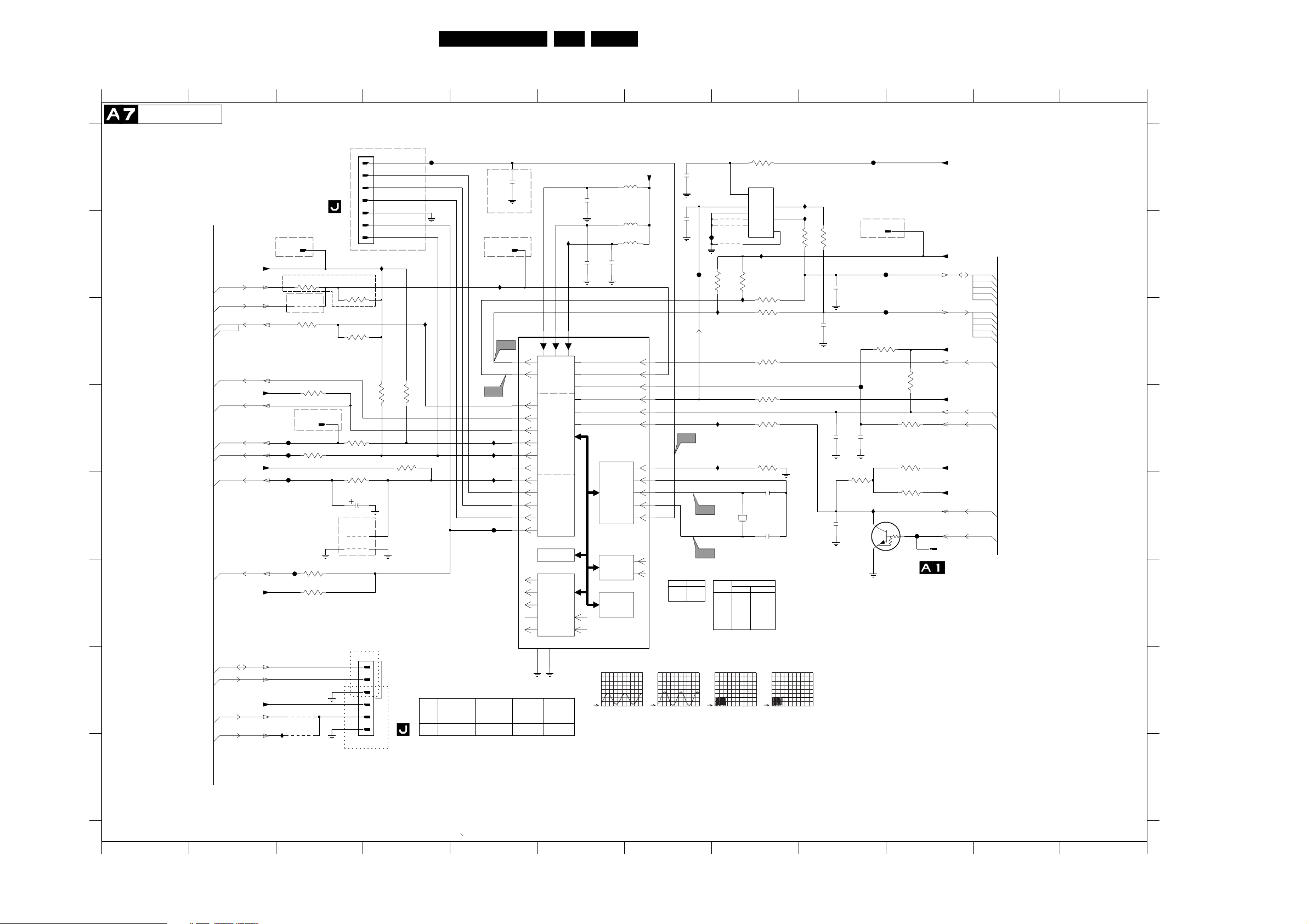
Large Signal Panel: Control
123456789101112
CONTROL
A
B
A13-2
A13-75
SEL-IF-LL_M-TRAP
A4-3
C
D
E
F
G
H
A5-3
A12-4
A1-5
SEL-MAIN-FRNT-RR
A10-12
A8-7
A8-15
Treble_Buzzer_Hosp-app
A8-6
A7-14
A7-13
A5-44
A6-17
VlotAux+5V
STATUS2
ITV_MSG
LED
+3.3V
Stdby_con
Bass_panorama
+3.3V
Volume|Mute
+3.3V
FMR
SANDCASTLE
SDA
SCL
+8V
FOR ITV ONLY
0250
3635 100R
FOR ITV ONLY
9647
3636
100R
FOR ITV ONLY
F604
F603
F613
F602
4618
4604
I610
Schematics and PWB’s
FOR ITV ONLY
POR
1
DATA - OU T
2
DATA - IN
3
CLOCK
4
GND
5
TREBLE-BUZZ
6
Bass_panorama
7
I615
TO 0240
OF
SET WITH SVHS
3601 8K2
0240
3612
*
3605
4K7
3619
8K2
*
0261
3609
*
3617
*
4K7
3615
*
10K
3614
*
4K7
1K
3618
10K
2604
10u
SDM
9641
2 9631 1
0217
1
2
3
4
5
6
FOR ITV ONLY
FOR
COMPAIR
3610
*
3623
4K7
TO 0217
OF
F612
I617
8K2
Diversity Table
ITEM
BG.I.DK/M-
3612
IF-38.9-
QSS
AP
8K2
FOR ITV ONLY
FOR ITV ONLY
0273
I616
C4
I613
I612
I606
F614
IF-38.0-
BG.I.DK/M-
QSS
CH
8K2
2616
7200-B
TDA95XX
C5
71
3V7
72
3V7
3
0V
5
3V2
6
3V3
70
5V
78
0V
79
73
0V
74
0V
75
0V
76
0V
77
0V
47n
SCL
SDA
R
G
B
BL
COR
IF-38.0-
BG.I.DK /
M-MN
CH
8K2
61
66
3V2
3V3
IIC-BUS
TRANSCEIVER
I/O
PORTS
VST PWM-DAC
ROM/RAM
OSD
TELETEXT
DISPLAY
7
4
0V
0V
IF-38.9
BG.I.DK /
M-MN
AP
8K2
I614
3V2
37L01.2A 7.
0217 G3
0240 A3
0250 B3
0261 D3
0273 B5
0274 B9
0303 E10
1660 E8
2601 A7
2602 D9
2604 E3
2606 E9
2607 E8
2608 A6
2609 E8
2611 B6
2612 C9
2613 B9
2615 B7
2616 A5
2618 B6
2619 D9
3601 B3
3603 B9
3604 B8
3605 C3
3606 B8
3607 B8
3608 D10
3609 D3
3610 D4
3611 A8
3612 C3
3614 F3
3615 F3
3617 D3
3618 E3
3619 D4
3622 D8
3623 D4
3624 C8
3625 B8
3626 D8
3627 C10
3628 D8
3629 C10
3630 E9
3632 E10
3633 D10
3634 C8
3635 B3
3636 C3
4601 B8
4602 B8
4603 B8
4604 H3
4618 G3
5602 A7
5603 B7
5604 B7
7200-B C5
7602 A8
7606 E10
9631 E3
9641 E3
9647 C3
F602 F3
F603 D3
F604 D3
F605 D9
F606 A9
F607 E10
F608 B7
F609 B7
F610 C9
F611 B10
F612 A4
F613 E3
F614 E5
I601 A9
I602 B9
I603 B8
I604 C8
I605 C8
I606 E5
I607 E9
I608 D8
I609 D8
I610 H3
I612 D5
I613 D5
I614 B6
I615 B4
I616 B5
I617 C4
68p
1u
2606
F606
FOR ITV ONLY
0274
F605
100p
2602
3630
2K2
I607
F611
F610
3629
RES
7606
RES
3627
3608
100R
3633
RES
3632
0R
F607
4K7
0303
to 0302 of
+3.3V
+3.9V
SDA
A4-14
A7-14
A9-14
A11-14
SCL
A4-13
A7-13
A9-13
A11-13
+3.3V
STATUS1
N.C.
(FOR E/W ONLY)
+3.3V
POWER_DOWN
A1-11
IR
A12-10
+3.9V
+3.3V
KEYBOARD_protn
A12-80V
EW_protection
N.C.
A
B
C
D
E
F
3611
4601
4602
4603
2K2
3V3
8
3V3
7
4
3
2
3607
I605
1660
dBX PCB
Mono
---
--YES
YES
YES
YES
100R
#
7602
I603
2K2
3625
12MHZ
Stereo
EEPROM
100R
YES
YES
3624
100R
3634
RES
3626
4K7
3622
3628
10K
2607
2609
---
---
---
---
*
*
6
5
M24C08
1
100R
C5
3V7
3V7
I601
I602
3604
100R
3603
2612
100R
2613
68p
2619
1n
+3.3V
5602
2601
220n
5u6
1u
2608
2618
5603
5u6
5604
5u6
1u
1u
2611
2615
1n
F608
F609
**
*
3606
I604
59
1
0V
2
0V
3V3
67
68
0V
69
3V2
80
3V3
I608
C3
AP
33pF
I609
C1
C2
Diversity Table
ITEM
3609
3610
3614
3615
3617
3619
C4
H
V
ENHANCED
80C51
CPU
TELETEXT
ACQUISITION
1/10 PAGES
MEMORY
C1
CVBS
SYNC
60
0V
62
0V
1V5
63
64
0V
65
C2
Diversity Table
ITEM
2607
2609 33pF
G
1V / div DC
500us / div
1V / div DC
500us / div
2V / div DC
200us / div
2V / div DC
200us / div
H
CL 16532101_031.eps
1
2345678910
11 12
230801
Page 58
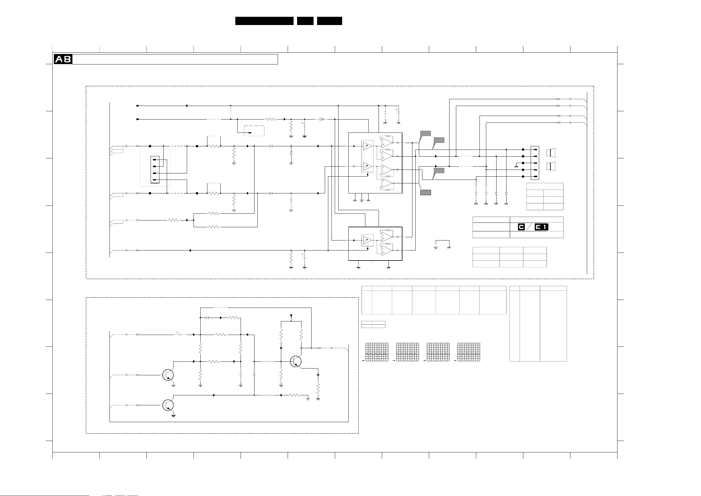
Schematics and PWB’s
Large Signal Panel: Audio Amplifier + Mono Sound Processing
123456789101112
AUDIO_AMPLIFIER + MONO_SOUND_PROCESSING
A
B
C
D
E
F
G
AUDIO AMPLIFIER
MainAux
VlotAux+5V
Main_OutL
A8-45
A9-45
A11-45
Main_OutR
A9-46
A11-46
Treble_Buzzer_Hosp-app
A7-6
A8-6
Volume|Mute
A7-15
F901
FOR ITV ONLY
0271
F903
MONO SOUND PROCESSING
MONO|AM_MONO_SOUND
A5-43
Bass_panorama
A7-7
Treble_Buzzer_Hosp-app
A8-6
I901
9921
*
4902
4901
1
2
3
4
4903
3921
330K
F902
F904
I908
I909
3903
4904
3905
3922
330K
3923
330K
2942
*
2941
I942
*
*
3943
I944
0V
0V
0V
7941
*
0V
7942
*
3946
3945
*
I946
4921
*
*
*
*
4941
I941
3904
3906
3941
*
3942
*
I945
*
FOR ITV ONLY
0275
I904
10K
I906
*
I943
*
3944
**
2943
2944
2946
*
2945
*
3901
1K
2904
*
2906
*
3948
I948
3949
I947
I903
1V8
*
3902
2905
2907
3907
+8V
3947
38L01.2A 7.
0246 B11
0271 B3
0275 B5
2901 B8
2902 B8
2903 B6
2904 B5
2905 B6
2906 C5
2907 C6
A
AmpOutR+
AmpOutL+
RES
470u
2902
3V7
STB
5
2901
1
5
8
11V8
VCC
2
CH1+
4
CH1-
10CH2-
12CH2+
2
CH1+
4
CH1-
GNDCH1
3
5V2
5V2
5V2
5V2
A1
A2
I910
I911
A3
A4
9901
*
9902
*
AmpOutR_Pos
AmpOutR_Neg
2947
With Side AV + HP
Without Side AV + HP
AmpOutL_Pos
100p
2948
0246
*
*
STEREO
MONO
AmpOutL_Neg
100p
2949
2950
100p
AN7522N
100p
To
To Speaker
7901
-
F906
F905
F909
F908
F907
0246
*
5
4
3
2
1
2 X 5W
2 X 3W
2 X 1W
7902
-
AN7523N
SPEAKER
16 ohm
8 ohm
8 ohm
Of 0254
6901
BAS216
1u
3K3
2903
I905
1n
I907
1n
*
10u
2908
1V4
1V4
0V3
7901
*
AN7522N
6 CH1-IN
8 CH2-IN
9VOL
GNDCH111GNDCH2
3
7902
*
AN7523N
6 CH1-IN
9VOL
GNDINP NC
GNDINP
7
STB1VCC
7
AmpOutL_Pos
AmpOutR_Neg
A12-70
A12-71
A12-73
A12-72
B
C
D
E
6V2
3950
1V3
AUDIO AMPLIFIER
Mono Amp 1W
ITEM
2904
2906
3903
3905
3906
7901
7902
ITEM GLOBAL
3907 8K2
**
Main_OutL
A8-45
7943
*
A1
2V / div DC
5us / div
Mono Amp 3W Mono Amp 4W CH Mono Amp 4W EU Stereo Amp 1W Stereo Amp 3W/5W
1uF
8K2
YES
---
---
---
---
1uF
---
4K7
---
---
---
YES
A2
2V / div DC
500us / div
1uF
---
6K8
---
---
YES
---
A3 A4
2V / div DC
500us / div
1uF
8K2
YES
470nF
---
---
---
---
470nF
15K
15K
10K
YES
---
2V / div DC
500us / div
470nF
470nF
3K3
3K3
10K
YES
---
MONO SOUND PROCESSING
ITEM
2941
2942
2943
2944
2945
2946
3941
3942
3943
3944
3945
3946
3947
3948
3949
3950
3951
4941
7941
7942
7943
WITH STEREO
1uF
33nF
100nF
47nF
10nF
1uF
100R
3K9
2K7
2K7
1K
18K
330R
47K
15K
560R
390R
--BC847B
BC847B
BC847B
WITHOUT STEREO
10uF
---
---
---
---
---
---
---
---
---
---
---
---
---
---
---
---
JUMPER
---
---
---
F
G
I949
*
3951
2908 E6
2941 F3
2942 F4
2943 G4
2944 G5
2945 G5
2946 G5
2947 C9
2948 C10
2949 C10
2950 C10
3901 B5
3902 B6
3903 B4
3904 B4
3905 C4
3906 C4
3907 E6
3921 D3
3922 D4
3923 D4
3941 F4
3942 F4
3943 G4
3944 G4
3945 G4
3946 G4
3947 G6
3948 F5
3949 G5
3950 F6
3951 G6
4901 B3
4902 B4
4903 C3
4904 C4
4921 B4
4941 F4
6901 B6
7901 B7
7902 D7
7941 G3
7942 H3
7943 G6
9901 B9
9902 C9
9921 B4
F901 B3
F902 B4
F903 C3
F904 C4
F905 B11
F906 B11
F907 C11
F908 C11
F909 C11
I901 A3
I903 B5
I904 B5
I905 B6
I906 C5
I907 C6
I908 D3
I909 D3
I910 B9
I911 C9
I941 F4
I942 F3
I943 F5
I944 G3
I945 G4
I946 G4
I947 G5
I948 G5
I949 G6
*
H
H
(Mono sets only)
CL 16532101_032.eps
230801
123456789101112
Page 59

Schematics and PWB’s
Large Signal Panel: NICAM + 2CS + BTSC (Stereo / SAP Decoder)
123456789101112
NICAM + 2CS + BTSC (STEREO/SAP) DECODER
A
+5VA
VlotAux+5V
6u8
5831
B
VlotAux+5V
C
10u
2845
2844
D
E
G
H
MONO|AM_MONO_SOUND
A9-43
SC1_LIN
A10-47
SC1_RIN
A10-48
+5VA
QSS_AM_DEM_OUT
A5-42
A11
*
I855
2855
*
27p
12u
5835
*
3843
*
RES
4834
F
A5-44
VlotAux+5V
ITEM ST-BTSC
2855
2856
2857
2860
3843
5835
FMR
33p
47p
150p
180p
2K2
12u
*
2846
2859
150p
2857
*
1n
I838
5833
3u3
100u
ITEM RF-Mono AV-Stereo
2847 YES
3834 YES
A13
2K2
3834
100R
3835
RES
2860
YES
YES
2856
15p
*
+5VA
I839
2896
2847
*
1u
2848
RES
*
7835
4K7
3840
BC847B
*
I847
4V8
RES
8K2
4835
3841
*
*
4836
ITEM
QSS interC RD no-RD
---
2855
---
2856
---
2857
---
2858
---
2859
---
2860
---
3840
---
3841
---
3843
---
3849
---
4835
5835
---
7834
---
7835
I840
4V9
4V1
---
---
---
---
---
---
---
---
---
---
---
------
---
---
7834
BC847B A8
4V9
I848
4V1
2858
*
1u
3849
470R
I851
*
MN
---
---
---
---
---
---
---
YES
---
YES
---
---
---
YES
---
YES
---
---
---
YES
---
YES
---
---
---
YES
---
YES
2834
6831
1N4148
3831
47K
2897
390p
100n
*
0V
QSS interC RD
YES
YES
YES
---
---
82p
---
---
---
---
---
YES
---
---
YES
YES
YES
---
---
56p
---
---
YES
---
---
YES
---
---
470p
A5
ST
2835
I850
YES
YES
YES
YES
YES
YES
YES
YES
YES
YES
YES
I837
2833
47p
---
---
---
I831
I832
220p
2V6
1V5
1V5
3V8
3V8
3V8
no-RD
YES
YES
YES
YES
YES
2836
2837
3842
1K
---
---
---
---
---
---
---
---
---
43
47
48
44
41
42
39
40
1n5
4u7
2841
I852
6V2
CAPL_M
VREFTOP
SOUND IF
ANA_IN1+
ANA_IN1-
MONO
MONO-IN
SC1-IN-L
SCART 1
SC1-IN-R
SC2-IN-L
SCART 2
SC2-IN-R
I854
ITEM
2851
2852
2853
2854
3836
3837
3838
3839
4831
4832
4833
7832
7833
10u
0V
12
2843
10u
2842
100n
0V
TESTEN
DEMODULATOR
Mono
YES
YES
YES
1617
0V
DVSS
DVS UP
& NICAM
DECODER
18 19
---
---
---
---
---
---
---
---
---
---
39L01.2A 7.
I836
45 46
0V
3V8
AVS S
AGNDC
A/D
A/D SCART-R
21 22
Stereo
SC-R
CN-R
YES
YES
YES
YES
YES
YES
YES
YES
YES
YES
YES
YES
YES
YES
YES
YES
YES
---
---
---
YES
---
---
YES
---
YES
5V
AVS UP
0V
SCART-L
SCART
2895
560p
2898
10n
2840
100n
7V8
AHVS S
FM1/AM
FM2
NICAM A
NICAM B
IDENT
A6
2V / div DC
200us / div
I835
F832
29
3334 3536
0V
VREF1
AHVS UP
LOUDSPEAKER L
LOUDSPEAKER R
DSP
Switching Facilities
NC
27 28
0V
VREF2
SCART-L
SCART-R
2894
220p
550 5123
20
0V
5V
5V
RESETQ
ADR_SEL
STANDBYQ
32
37 1
A7
2V / div DC
200us / div
1831 C9
2831 C9
2832 C9
2833 D5
2834 B5
2835 B5
2836 B5
2837 B5
2838 A10
2839 B10
A
2838
47p
3832
100R
2839
47p
3833
100R
+8V
SCL
SDA
A7-13
B
A7-14
C
Main_OutL
A8-45
Main_OutR
A8-46
3836
*
7832
BC847B
I841
1K
SC2_CTRL
+8V
SC1_LOUT
A10-50
A5-43
A9-43
A10-51
MONO|AM_MONO_SOUND
2851
*
4u7
D
E
*
+8V
*
7833
BC847B
I844
3838
2853
*
4u7
1K
SC1_ROUT
A10-49
F
*
2832
I843
I853
A6
A7
1831
18M432
HC-49/U
1p
3837
*
100R
A12
3839
*
100R
2831
2899
I842
I845
1p
10n
*
A10
A9
2852
2854
1n
1n
2887
*
*
*
10n
2849
1n
2850
1n
4832
4831
4833
F831
I833
I834
5832
6u8
7831
MSP34X5G
52678
2V4
3V7
3V7
2V4
AUDIO PLL
I2C_CL
I2C_DA
1V8
SC1-OUT-L
SCART
SC1-OUT-R
A11
25
1V8
24
2
0V
3
4
0V
9
10
TP
11
13
14
15
26
31
3V
3V
30
D/A
D/A
D/A
D/A
DACM-L
LOUDSPEAKER
DACM-R
49
38
*
1V / div DC
500us / div
G
H
2840 B7
2841 C6
2842 A6
2843 A6
2844 C4
2845 C4
2846 G2
2847 D4
2848 D4
2849 C10
2850 D10
2851 E11
2852 E9
2853 F11
2854 F9
2855 E2
2856 E3
2857 F3
2858 E4
2859 G2
2860 F3
2887 C10
2894 A8
2895 A7
2896 F3
2897 C5
2898 B7
2899 D9
3831 B5
3832 B10
3833 B10
3834 D3
3835 D3
3836 E10
3837 E9
3838 F10
3839 F9
3840 E4
3841 F4
3842 G5
3843 F3
3849 F4
4831 E10
4832 D10
4833 F10
4834 F2
4835 F4
4836 F4
5831 B4
5832 B8
5833 G3
5835 E3
6831 B5
7831 C8
7832 E10
7833 F10
7834 E5
7835 E4
F831 D10
F832 B7
I831 B5
I832 B5
I833 B8
I834 B8
I835 B7
I836 A6
I837 C5
I838 G3
I839 D3
I840 D4
I841 E10
I842 E9
I843 E9
I844 F10
I845 F9
I847 E4
I848 E4
I850 G5
I851 F4
I852 C6
I853 F9
I854 G6
I855 E3
12
CL 16532101_033.eps
230801
3456789101112
Page 60
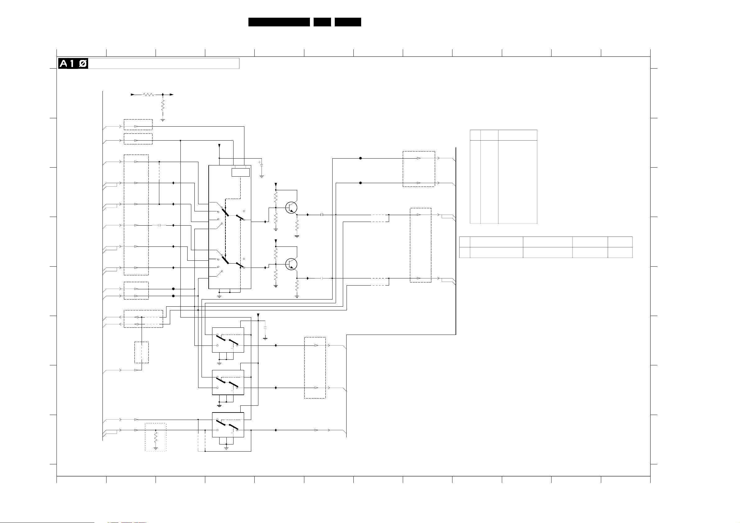
Schematics and PWB’s
Large Signal Panel: Audio / Video Source Switching
12345678910
AUDIO/VIDEO SOURCE SWITCHING
I801
4809
2803
100n
3802
+6V8
*
I803
I804
I805
I806
I807
F801
F802
0V
0V
2V4
1V8
0V
0V
2V4
1V7
1V6
3V8
1V6
1
5
2
4
12
14
15
11
3V8
12
13
2
1
G
A
B
C
D
E
F
+8V
From Micronas
A9-50
A7-12
A12-31
A13-32
A14-32
A13-52
A14-52
A12-53
A13-54
A14-54
A13-55
A14-55
A9-51
A9-49
A14-56
A14-57
Mono Scart1 out
(RF Mode always)
QSS_AM_DEM_OUT
A5-42
SC2_CTRL
SEL-MAIN-FRNT-RR
From MicroP
From Front/Rear I/O
LFRONT-IN
L1-IN
L2-IN
RFRONT-IN
R1-IN
R2-IN
From Micronas
SC1_LOUT
SC1_ROUT
Stereo Scart1 Out (RF Mode always)
L1-OUT
R1-OUT
*
4806
3801
*
*
*
4805
9801
+6V8
VDD
7801
*
LL
LH
HL
HH
LL
LH
HL
HH
VSS
Y0
Y1
Vss
8
Y0
Y1
Vss
8
5V8
8
*
*
VEE
7802-A
Vee
7
7802-B
Vee
7
8V
7
E
6
E
6
916
LOGIC
Vdd
Vdd
5V8
5V8
40L01.2A 7.
11 12
A
For Audio
Mono Set
ITEM
AP/NA/LA
2801
---
2802
F803
10
0V
LSBMSB
H
L
H
L
6
16
5V
S
11
1V6
Z
14
16
5V
S
10
1V6
Z
15
*
2801
+6V8
5V8
*
3803
2V4
I808
2V4
3
2V4
13
+6V8
I809
2802
*
3804
+6V8
*
3806
2V4
*
3807
*
I814
I815
1V7
1V7
5V8
*
3805
*
3808
7803
I810
*
7804
I811
*
Only Europe
(Scart2 Out)
L2-OUT
R2-OUT
2804
*
2805
*
A14-62
A14-63
F805
4801
*
4802
*
4803
*
4804
*
To Micronas/BTSC/UOC
SC1_RIN
SC1_LIN
Monitor Out/AV Out
L-OUT
R-OUT
A9-48
A9-47
A13-60
A14-60
FOR VIDEO (AP/LATAM/NAFTA)
ITEM
4807
4808
7802
A13-61
A14-61
---
---
2804
2805
---
3801
---
3802
---
3803
---
---
3804
---
3805
---
3806
---
3807
3808
---
4801
---
4802
JMP
4803
---
---
4804
4805 --4806
---
7801
---
7802
---
7803
---
7804
---
9801
---
#
Only use if there is a Scart 2
1x Rear Video In With Front or
Side Video With SVHS / 2x Rear
Video With Front Or Side Video
Stereo Set
AP/NA/LA
22uF
220nF
4u7
4u7
220R
1K
100K
82K
1K
100K
82K
1K
---
JMP
---
JMP
---
---
HEF4052BT
REF. TO VIDEO TABLE
BC847B
BC847B
---
x
x
Y
1x Rear Video In With Front Or
Side Video W/O SVHS / 1x
Front Or Sideo Video IN
JUMPER
x
x
2x Rear Video In W/O
Front Or Side Video
x
JUMPER
x
No Video Input
x
x
x
B
C
D
E
F
G
2801 B5
2802 F5
2803 D3
2804 C6
2805 E6
3801 A2
3802 A3
3803 C5
3804 D5
3805 D5
3806 D5
3807 E5
3808 E5
3809 H2
4801 C7
4802 D7
4803 E7
4804 E7
4805 F2
4806 F2
4807 H3
4808 H3
4809 C3
7801 C4
7802-A F4
7802-B G4
7802-C G4
7803 C5
7804 D5
9801 F2
F801 E3
F802 E3
F803 B7
F805 C7
I801 A3
I803 C3
I804 C3
I805 D3
I806 D3
I807 D3
I808 D5
I809 D5
I810 C6
I811 E6
I814 F5
I815 G5
I816 H5
H
Vee
7
16
5V8
5V
Vdd
S
9
0V
Z
4
E
6
I816
SY_CVBS-IN
A12-58
A13-59
A14-59
CVBSFRONT-IN
Y_CVBS-IN
FOR EUROPE
SET ONLY
*
3809
4807
0V
0V
4808
7802-C
*
Y0
5
Y1
3
Vss
8
**
12345
A5-37
CL 16532101_034.eps
6 7 8 9 10 11 12
H
230801
Page 61

Schematics and PWB’s
Large Signal Panel: Front I/O + Front Control + Headphone
123456789101112
FRONT IO + FRONT CONTROL + HEADPHONE
A
FRONT CINCH
C
D
G
H
MONO SET
0218-C
0218-B
0218-A
9982
2
3
1
5
6
4
8
9
V
B
*
0277-B
*
0277-A
*
L
*
R
*
E
F
HEADPHONE
AmpOutL+
A8-71
*
AmpOutR+
A8-70
For Engg Purpose Only
F694
4694
F695
F181
1181
F182
1182
F183
1183
7
2981
I982
1u
2983
I984
1u
3181
2185
2186
75R
*
*
3981
120R
3982
120R
3182
100R
3183
*
3185
*
2982
2984
2181
3184
3186
I983
470p
I985
470p
41L01.2A 7.
0214 E10
0215 C5
0218-A C3
0218-B C3
0218-C B3
0219 D5
0232 F5
0239 B8
FRONT CONTROL
KEYBOARD_protn
A7-8
A12-8
I181
22p
RES
6181
I185
2184
*
330p
2182
*
2183
330p
I981
*
0292
FOR ITV ONLY
0215
1
2
3
FOR ITV ONLY
0219
6
5
4
3
2
1
0232
1
6
5
4
2
3
7
8
9
9181
0270
I182
I183
TO 0251 OF
TO 0251 & 0253 OF
CVBSFRONT-IN
LFRONT-IN
RFRONT-IN
OR
AmpOutL_Pos
A10-58
A11-58
A5-31
A10-31
A11-31
A10-53
A11-53
A8-73
A7-4
+3.3V
A7-10
KEYBOARD_protn
A12-8
Diversity Tables
For Front Cinch
ITEM
Mono Set GL Stereo Set GL
0218
0227
2184
I986
AmpOutR_Pos
A8-72
2185
2186
3813
3814
3185
3186
LED
IR
---
YES
2u2
---
---
150R
47K
---
---
F682
3685
POWER
RES
0239
1
2
3
FOR ITV ONLY
3695
100R
4692
4693
FOR ITV ONLY
0293
0286
*
1606
YES
---
2u2
---
---
150R
47K
150R
47K
TS
F691
I681
I682
I691
6691
3692
4691
2694
3684
**
channel+
1603
FOR ITV ONLY
4695
3691
330R
LTL-10224WHCR
*
RES
2692
RES
RES
2695
2696
EUAP
---
1K
3681
*
I683
channel-
1602
4K7
3694
3
1
C6
RES
Stereo HPITEM Mono HP
2
RES
1
+3.3VA
F684
2
F692
3
4
5
---
F683
volume+
1601
I685
*
3686
I693
VS
OUT
GND
6692
TSOP1836
0214
3682
6681
BAT85
3683
USA
F693
F696
RES
2693
HEADPHONE
9982 JMP
Note that for Non-Headphone set, non of the components are in
FRONT CONTROL
ITEM
3692
FRONT CONTROL
ITEM PAINTER LEADER PAINTER PLUS
3681 470R 390R
3682 3K9 3K3
3683 270R 390R
3684 470R 560R
3685 560R 560R
3686 1K8 1K5
*
FOR ITV ONLY
1
2
3
4
5
I684
3693
2691
0259
volume-
1600
220R
100u
TO 0259
OF
A
B
C
D
E
F
G
H
0259 E11
0270 B6
0277-A B2
0277-B C2
0286 E8
0292 F5
0293 E8
1181 B3
1182 B3
1183 C3
1600 B11
1601 A10
1602 A10
1603 A9
1606 B8
2181 B4
2182 B4
2183 C4
2184 B5
2185 B4
2186 C4
2691 D11
2692 D9
2693 F9
2694 F9
2695 F9
2696 F9
2981 F3
2982 F4
2983 G3
2984 G4
3181 B4
3182 B4
3183 B4
3184 B4
3185 C4
3186 C4
3681 A10
3682 A11
3683 A9
3684 A9
3685 A8
3686 B10
3691 C9
3692 D9
3693 C11
3694 C10
3695 C8
3981 F4
3982 G4
4691 D9
4692 D8
4693 D8
4694 H2
4695 C9
6181 B4
6681 B11
6691 C9
6692 D10
9181 B6
9982 F3
F181 B4
F182 B4
F183 C4
F682 A8
F683 A10
F684 E10
F691 D9
F692 E10
F693 D9
F694 H2
F695 H2
F696 E9
I181 B5
I182 B6
I183 C6
I185 B5
I681 A8
I682 A9
I683 A10
I684 A11
I685 B10
I691 C9
I693 C10
I981 E5
I982 F3
I983 F4
I984 G3
I985 G4
I986 G5
CL 16532101_035.eps
230801
123456789101112
Page 62

Large Signal Panel: Rear I/O CINCH
123456789101112
REAR I/O CINCH
A
MONITOR OUTPUT
V
B
C
D
E
F
G
H
L
R
YUV INPUT
Y
U
V
V
L
R
AV1 INPUT BLOCK
ITEM MONO STEREO
2124
2125
3125
3126
0223-D
0223-C
AV1
0223-B
---
---
---
---
Schematics and PWB’s
MONITOR OUTPUT BLOCK
ITEM
---
2104
---
2106
---
3105
3106
---
F101
16
F102
14
4101
**
2
F103
4102
4104
*
F104
F105
F106
3
4
1107
2127
1108
1109
2128
MainSupplyGnd
I107
5
0242
FOR ITV ONLY
RES
RES
15
13
12
10
11
9
INPUT
8
6
7
5
330pF
2u2
150R
47K
SET
WITH
VIDEO
OUT
RES
1
0226
F107
F108
F109
1101
1102
11031105
1104
1106
1
3123
150R
3125
STEREOMONO
2
*
F116
SET WITH VIDEO OUT
330pF
10uF
150R
220K
RES
2107
RES
2108
9103
RES
RESRESRES
3111
9102
RES
3113
9101
RES
3115
I108
I109
34567
*
3121
330p
2122
2124
*
3101
68R
3103
150R
3105
*
TO 0242 OF
3122
*
3124
3126
*
47K
2121
2102
2103
2104
3114
3116
3112
RES
9111
RES
RES
9112
RES
9113
RES
*
*
22p
330p
I110
I111
I112
3102
3104
3106
TO 0262
OF
*
2111
2112
2113
2101
1K
220K
2123
2u2
2125
*
0262
+8V
I101
2105
10u
2106
RES RESRES
F117
89
67
7V6
470n
2V9
*
3151
3152
3153
1
2
3
3V5
7101
BC847B
2V9
I102
I103
I104
RES
I105
RES
I106
RES
FOR ITV ONLY
V_OUT
L-OUT
R-OUT
G_Y-IN
B_U-IN
R_V-IN
FBL-1
CVBS1-IN
L1-IN
R1-IN
ITV_MSG
A5-40
A10-60
A11-60
A10-61
A11-61
A5-33
A5-34
A5-35
A5-39
A5-38
A5-32
A10-32
A11-32
A10-54
A11-54
A7-75
42L01.2A 7.
A10-52
A11-52
A10-55
A11-55
A5-30
A10-59
A11-59
9121
*
9122
*
A5-41
A7-2
L2-IN
R2-IN
C-IN
Y_CVBS-IN
V1-OUT
STATUS2
FOR ITV ONLY
0227
1
2
345
2132
2u2
2134
I115
I116
I117
TO 0227 OF
I113
I114
*
SET WITH SVHS
2135
2136
4121
FOR ITV ONLY
2141
6
F115
100R
22p
*
7
330p
AV2 INPUT BLOCK
MONO
ITEM
---
2133
---
2134
---
3133
---
3134
47K
2131
3132
**
3134
2133
3136
3135
3138
*
3137
*
3
4
5
6
TO 0242 OF
3141
F114
1K
330p
75R
STEREO
330pF
2u2
150R
47K
3131
150R
3133
*
F112
F113
1
2
1115
ITEM
2121
2136
3121
3122
3137
3138
0229
2137
2138
1x Rear Video In
With SVHS
x
22p
x
x
75R
100R
1110
F110
RES
1111
F111
RES
1112
4131
6
1113
11
1114
W/O SVHS
22p
x
75R
10R
x
x
2x Rear Video in No Rear Video Inputs1x Rear Video in
AV2
0223-A
4
2
3
1
0269
(FOR SETS WITH 9 + 3 P CINCH)
SET WITH
AV2 W/O SVHS
C
Y/CVBS
5104
9
0225-B
GLOBAL
9121 JUMPER
9122
GLOBAL
ITEM WITH YUV WITHOUT YUV
4102
4104
JUMPER
JUMPER
JUMPER
SVHS
8
3
7
2
1
0225-A
22p
22p
75R
10R
75R
100R
INPUT
V
L
R
---
---
0223-A B11
0223-B F3
0223-C C3
0223-D B3
0225-A D11
0225-B D10
0226 E3
0227 A7
0229 F9
x
x
x
x
x
x
A
B
C
D
E
AV1 INPUT WITHOUT SVHSAV1 INPUT WITH SVHSITEM
---
---
F
G
H
CL 16532101_036.eps
230801
0242 E4
0262 H6
1101 B4
1102 B4
1103 C4
1104 C4
1105 D4
1106 D4
1107 F3
1108 G3
1109 G3
1110 B10
1111 B10
1112 C10
1113 D10
1114 D10
1115 G9
2101 A5
2102 B5
2103 B5
2104 C5
2105 B6
2106 C6
2107 B4
2108 C4
2111 C5
2112 D5
2113 D5
2121 F5
2122 G4
2123 G5
2124 G4
2125 G5
2127 G4
2128 G4
2131 B9
2132 B8
2133 C9
2134 C8
2135 D8
2136 D8
2137 B9
2138 C9
2141 G8
3101 B5
3102 B5
3103 B5
3104 B5
3105 C5
3106 C5
3111 C4
3112 C5
3113 D4
3114 D5
3115 D4
3116 D5
3121 F4
3122 F5
3123 G4
3124 G5
3125 G4
3126 G5
3131 B9
3132 B9
3133 C9
3134 C9
3135 D9
3136 D9
3137 D9
3138 D9
3141 G9
3151 C6
3152 D6
3153 D6
4101 C3
4102 C4
4104 C3
4121 F8
4131 C10
7101 B6
9101 D4
9102 D4
9103 C4
9111 C5
9112 D5
9113 D5
9121 F7
9122 F7
F101 B4
F102 B4
F103 C4
F104 C4
F105 D4
F106 D4
F107 F3
F108 G3
F109 G3
F110 B10
F111 C10
F112 D9
F113 D9
F114 G9
F115 B8
F116 H4
F117 E6
I101 B6
I102 B6
I103 C6
I104 C6
I105 D6
I106 D6
I107 E4
I108 E4
I109 E4
I110 F5
I111 G5
I112 G5
I113 B8
I114 C8
I115 D8
I116 D8
I117 G8
123456789101112
Page 63

Schematics and PWB’s
Layout Large Signal Panel (Top View)
43L01.2A 7.
0211 A2
2521 B3
3508 B3
7408 C5
7471 B7
7515 B4
7520 B3
7521 A3
7540 B4
7560 C4
7602 D5
7831 D2
7901 D3
7902 D3
9001 E5
9101 D6
9102 D6
9103 D6
9111 D6
9112 D6
9113 D6
9121 C6
9122 C6
9171 C6
9172 C6
9173 D6
9174 D6
9175 D6
9177 D6
9181 C1
9182 C1
9183 C1
9191 B1
9192 B1
9193 B1
9200 E4
9298 E6
9299 E5
9401 C6
9402 B5
9403 B5
9404 B5
9405 A5
9408 A5
9420 B4
9421 A5
9425 C5
9426 C5
9427 B5
9428 C5
9430 C5
9431 B5
9432 C5
9433 B5
9434 B5
9471 C6
9500 A2
9501 A2
9502 B3
9503 B2
9504 C3
9505 C4
9506 C4
9507 C4
9508 C4
9509 B4
9510 C4
9511 C5
9512 B2
9513 A3
9514 B3
9517 B3
9520 A3
9521 A3
9522 B4
9523 C4
9524 C4
9610 E3
9611 C4
9612 C4
9613 D4
9614 E4
9615 D5
9616 D5
9617 D3
9618 D5
9619 D3
9620 D5
9621 D5
9622 C4
9623 E5
9624 D3
9625 E6
9626 D3
9627 D3
9628 E5
9629 D5
9630 C3
9631 D5
9632 E4
9633 D4
9634 D4
9635 D4
9636 C4
9637 E5
9638 D4
9639 D3
9640 D5
9641 D5
9642 D5
9643 D3
9644 E3
9645 E3
9647 D5
9648 E5
9650 E6
9653 C3
9654 C4
9655 C5
9656 C5
9657 D4
9658 C5
9659 C5
9660 C5
9661 D5
9662 D5
9663 D5
9664 C5
9665 C4
9666 C5
9668 C4
9669 C4
9670 C4
9672 C5
9673 C3
9674 C4
9675 C5
9676 C5
9678 C5
9679 C5
9680 D3
9682 C4
9683 D3
9684 D3
9685 D5
9686 D5
9687 D4
9688 D4
9689 D5
9690 D3
9691 E5
9692 C3
9693 C3
9694 E5
9695 E5
9696 E6
9697 D5
9698 D5
9699 C1
9801 D3
9811 C3
9812 D3
9813 D3
9814 D3
9815 D3
9816 C2
9817 C3
9818 C3
9820 C2
9821 C3
9822 D3
9824 C3
9825 C3
9826 C3
9827 D2
9828 D2
9829 D2
9830 C2
9832 C2
9833 D1
9901 D3
9902 E3
9911 D3
9912 D3
9913 E3
9914 E3
9915 E3
9916 D3
9917 D3
9921 D3
9982 B1
9991 B1
9993 E6
9994 E3
9996 E5
9997 E7
9998 E4
CL 16532053_001.eps
170501
0212 B2
0213 B2
0214 B1
0215 B1
0217 E3
0218 C1
0219 B1
0220 A6
0221 A5
0222 C6
0223 D6
0225 C6
0226 D6
0227 C6
0229 C6
0231 A2
0232 B1
0239 C2
0240 D5
0242 D6
0243 D4
0246 E3
0248 E4
0249 D4
0250 C5
0251 C3
0259 B1
0261 D4
0262 D6
0265 E7
0266 E4
0270 B1
0271 E3
0273 D5
0274 C5
0275 D3
0276 D4
0277 B1
0282 C4
0283 E6
0285 E6
0286 C2
0292 B1
0293 C1
1000 E6
1002 E5
1003 E5
1004 E4
1200 E4
1201 E4
1202 E3
1203 E5
1500 A2
1515 C2
1600 C1
1601 C1
1602 D1
1603 D1
1606 A1
1660 D4
1831 C1
2005 E6
2006 E6
2008 E6
2105 D6
2106 D6
2209 D4
2210 D4
2216 E4
2220 D3
2229 E4
2230 E4
2235 E4
2244 E4
2246 E5
2247 E5
2250 E5
2400 B6
2401 A4
2402 A4
2404 A4
2407 B5
2408 A5
2409 B5
2410 C5
2411 B5
2412 B5
2413 A6
2414 B6
2416 A5
2417 B6
2419 B5
2420 C5
2422 C6
2423 C6
2424 B5
2471 B6
2472 B6
2473 B6
2476 C7
2500 A2
2501 B2
2502 B3
2503 A3
2504 A4
2505 B2
2506 B3
2507 A3
2508 A3
2515 A4
2516 B3
2523 A3
2560 A4
2561 A4
2562 B4
2563 B4
2564 B4
2565 A4
2566 B4
2567 C4
2568 B4
2580 C3
2604 D4
2691 A1
2801 D3
2837 D2
2841 C2
2843 C2
2844 C2
2846 C1
2855 C2
2902 D3
2903 D3
2908 E3
2941 E3
2981 B1
2983 B1
3000 E6
3001 E6
3005 E4
3101 D6
3103 D6
3105 D6
3111 D6
3112 D6
3113 D6
3114 D6
3115 D6
3116 D6
3121 D6
3122 D6
3123 C6
3125 C6
3131 C6
3133 D6
3135 C6
3136 C6
3137 C6
3138 C6
3141 C6
3181 B1
3182 B1
3183 C1
3185 C1
3200 E4
3201 D4
3202 D4
3203 D4
3204 D4
3207 E4
3210 E4
3211 E4
3213 E4
3216 E3
3220 D4
3221 E3
3222 D4
3228 E4
3235 D4
3244 E5
3249 E5
3250 E5
3251 E4
3401 B5
3402 C5
3403 A5
3404 B4
3405 B5
3406 B4
3407 A5
3408 C4
3411 B5
3412 B5
3414 B5
3415 C5
3416 A6
3417 B6
3421 C5
3424 C5
3425 B5
3427 C6
3428 C6
3429 B5
3430 B5
3432 B5
3471 C6
3472 C6
3473 C6
3474 C6
3475 C6
3476 C6
3477 C6
3478 C6
3479 B6
3500 A1
3501 B2
3502 B3
3503 B3
3504 B3
3505 B2
3506 A2
3507 B2
3519 B3
3521 B3
3523 B3
3526 B3
3527 B3
3543 B4
3544 B3
3547 A4
3549 B4
3550 C4
3558 C4
3560 B4
3561 B4
3564 B4
3565 C4
3570 C3
3601 D5
3603 D5
3604 D5
3606 D5
3607 D5
3608 D4
3609 D5
3610 D5
3612 E5
3614 D5
3615 D5
3617 D5
3618 D5
3619 D5
3624 D5
3625 D5
3634 D5
3635 D5
3801 D3
3802 D3
3808 C3
3832 D2
3833 D2
3834 C2
3836 C2
3837 C2
3839 C2
3981 B1
3982 B1
5001 E5
5002 E5
5201 E4
5202 E4
5241 E5
5242 E5
5401 B5
5403 B5
5406 B5
5408 A5
5410 C6
5444 C5
5445 A6
5471 C6
5500 B2
5501 B2
5502 B2
5520 A4
5521 A3
5560 A4
5561 B4
5562 B4
5563 A4
5602 D5
5603 D4
5604 D4
5831 D2
5832 C2
5833 C1
6001 E6
6401 A5
6402 B5
6404 B5
6405 B6
6409 A7
6410 B5
6412 B5
6413 A7
6414 B5
6419 C6
6420 C5
6423 C5
6471 B6
6472 C6
6473 C6
6500 A3
6501 B3
6502 B3
6503 B3
6520 B3
6521 A3
6523 B3
6540 B4
6541 B4
6560 A4
6561 A4
6562 B4
6564 B4
6681 D1
6691 A1
6692 B1
6831 D2
7402 A5
7403 C4
7404 C5
7407 C6
Page 64
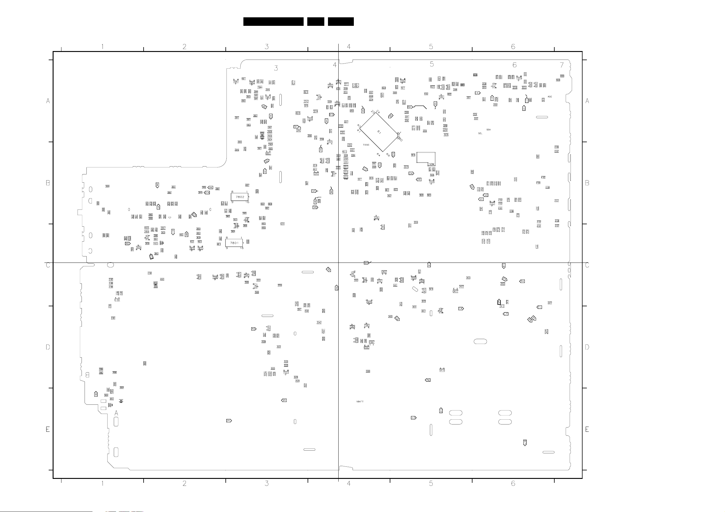
Schematics and PWB’s
Layout Large Signal Panel (Overview Bottom View)
Part 1
CL 16532053_02a.eps
Part 3
CL 16532053_02c.eps
44L01.2A 7.
2001 A6
2802 C2
3419 C5
4212 A4
4213 A4
4214 B3
4216 A6
4217 A3
4410 C5
4501 D4
4601 B5
4602 B5
4603 B4
4604 A3
4608 A7
4609 A7
4613 B4
4614 A3
4615 B5
4616 B4
4617 A5
4618 A3
4619 A4
4622 A5
4623 A5
4691 E1
4692 C2
4693 C2
4694 B1
4695 E1
4801 B3
4802 B3
4803 B3
4804 B3
4805 B3
4806 C3
4807 B3
4808 B3
4809 C3
4811 B3
4812 B3
4813 B2
4814 C2
4831 C2
4832 C2
4833 C2
4834 C2
4835 C2
4836 C1
4901 A3
4902 A3
4903 A3
4904 A3
4911 A3
4921 B3
4941 A3
4982 E1
5003 A4
5835 C2
6002 A6
6003 A6
6004 A5
6005 A5
6181 C1
6201 B4
6202 B4
6206 B4
6241 C4
6406 C4
6407 C4
6408 C5
6415 C5
6416 D5
6417 C5
6522 D3
6563 D4
6565 C4
6566 C3
6567 D4
6569 D4
6570 C3
6580 C2
6581 C2
6901 B3
7001 A5
7002 A5
7101 B6
7200 B4
7201 A4
7202 A4
7203 A4
7204 B4
7205 A4
7206 A4
7208 A4
7209 A6
7210 A6
7241 B4
7401 C4
7405 D5
7406 C5
7409 C5
7522 D3
7541 C3
7542 C3
7561 C4
7562 D4
7564 D4
7580 C2
7606 B5
7801 C3
7802 B3
7803 C3
7804 B3
7832 C2
7833 C2
7834 C1
7835 C2
7941 A3
7942 A3
7943 A3
CL 16532053_02b.eps
Part 4
CL 16532053_02d.eps
Part 2
CL 16532053_002.eps
170501
2002 A6
2003 A5
2004 A6
2007 A6
2009 A5
2010 A6
2101 B6
2102 B6
2103 B6
2104 B6
2107 B7
2108 B7
2111 B6
2112 B6
2113 B6
2121 B6
2122 C6
2123 C6
2124 C6
2125 C6
2127 B7
2128 B6
2131 C6
2132 C6
2133 C6
2134 C6
2135 B6
2136 B6
2137 C7
2138 B7
2141 B6
2181 D1
2182 C1
2183 C1
2184 C2
2185 D1
2186 C1
2201 A4
2202 B4
2203 A4
2204 B4
2205 A5
2208 A4
2211 A4
2212 A3
2213 B4
2214 B4
2215 B4
2217 A4
2219 A5
2221 B4
2222 A6
2223 A6
2225 A4
2226 A4
2227 A4
2228 A4
2233 B4
2234 A6
2236 A6
2237 A6
2238 A6
2239 A6
2240 A6
2241 A5
2242 A5
2243 A5
2245 A4
2248 A5
2249 A5
2252 A5
2253 A5
2254 A5
2403 C4
2405 D5
2406 C4
2415 C5
2418 C6
2421 C5
2475 D6
2477 C6
2520 D3
2522 D3
2524 D3
2525 D3
2526 D3
2527 D3
2528 D3
2540 C4
2542 D3
2559 C3
2569 D4
2601 B4
2602 B4
2606 B5
2607 B4
2608 B5
2609 B4
2611 B4
2612 B5
2613 B5
2615 B4
2616 B5
2618 B4
2619 B5
2692 E1
2693 D2
2694 D1
2695 D1
2696 D1
2803 C2
2804 B3
2805 B3
2831 B1
2832 B1
2833 B1
2834 B2
2835 B2
2836 B2
2838 B2
2839 B2
2840 B2
2842 B2
2845 B2
2847 C2
2848 B2
2849 B2
2850 B2
2851 B2
2852 C2
2853 B2
2854 C2
2856 C2
2857 C2
2858 C2
2859 C1
2860 C2
2887 B2
2894 B2
2895 B2
2896 C2
2897 B2
2898 B2
2901 B3
2904 B3
2905 B3
2906 A3
2907 A3
2942 A3
2943 A3
2944 A3
2945 A3
2946 A3
2947 A3
2948 B3
2949 B3
2950 B3
2982 D1
2984 D1
3002 A6
3003 A6
3004 A6
3006 A5
3007 A5
3008 A5
3009 A5
3010 A6
3011 A6
3102 B6
3104 B6
3106 B6
3124 C6
3126 C6
3132 B6
3134 C6
3151 B6
3152 B6
3153 B6
3184 C1
3186 C1
3205 B4
3206 B4
3208 A4
3209 A4
3212 A4
3214 A4
3215 A3
3217 B4
3218 B4
3219 B4
3223 B4
3224 B4
3225 B4
3226 B4
3229 A4
3230 A4
3231 A4
3232 A4
3233 A6
3234 A4
3236 A6
3237 A6
3238 A6
3239 A6
3240 A6
3241 A5
3242 A3
3245 A5
3246 A4
3247 C5
3248 A4
3254 A5
3256 C4
3257 A5
3258 A5
3259 B5
3261 A5
3410 D6
3413 D5
3418 C5
3420 C6
3422 C5
3423 C5
3426 C5
3431 D5
3520 D3
3522 D3
3524 D3
3525 D3
3528 D3
3529 D3
3530 D3
3531 D3
3540 D4
3541 D3
3542 D4
3545 D4
3546 C3
3548 C3
3552 C3
3559 C4
3562 D4
3563 C4
3566 C3
3567 D4
3568 D4
3569 C3
3580 C3
3605 C4
3611 B4
3622 B5
3623 B5
3626 B4
3627 B4
3628 B4
3629 B4
3630 B5
3632 B5
3633 B5
3636 A5
3637 B3
3638 B4
3681 B1
3682 C1
3683 C1
3684 B1
3685 C2
3686 B1
3691 E1
3692 E1
3693 E1
3694 E1
3695 C2
3803 B3
3804 C3
3805 B3
3806 C3
3807 C2
3809 B3
3831 B2
3835 C2
3838 C2
3840 C2
3841 C2
3842 C1
3843 C2
3849 C2
3901 B3
3902 B3
3903 A3
3904 A3
3905 A3
3906 A3
3907 A3
3921 A3
3922 A3
3923 A3
3941 A3
3942 A3
3943 A3
3944 A3
3945 A3
3946 A3
3947 A3
3948 A3
3949 A3
3950 A3
3951 A3
4001 A5
4002 A5
4003 A5
4004 A5
4005 A5
4006 A5
4011 A5
4012 A5
4101 B6
4102 B6
4104 B6
4121 B6
4131 C6
4181 B5
4203 A4
4204 A4
4205 B4
4206 B4
4207 B4
4209 A4
4210 A4
4211 A4
Page 65

Schematics and PWB’s
Layout Large Signal Panel (Part 1 Bottom View)
45L01.2A 7.
Part 1
CL 16532053_02a.eps
170501
Page 66

Schematics and PWB’s
Layout Large Signal Panel (Part 2 Bottom View)
46L01.2A 7.
Part 2
CL 16532053_02b.eps
210501
Page 67

Schematics and PWB’s
Layout Large Signal Panel (Part 3 Bottom View)
47L01.2A 7.
Part 3
CL 16532053_02c.eps
170501
Page 68

Schematics and PWB’s
Layout Large Signal Panel (Part 4 Bottom View)
48L01.2A 7.
Part 4
CL 16532053_02d.eps
210501
Page 69

A
B
C
D
E
F
G
H
Schematics and PWB’s
49L01.2A 7.
CRT Panel
123456789101112
CRT PANEL
160V 160V
68R
6341
2344
6331
I331
6321
I321
6311
I311
1n
BAV21
BAV21
I335
BAV21
BAV21
3347
F305
6343
OLDGND
I310
220R
BZX284-C8V2
3337
1K5
3317
1K5
3327
1K5
I318
3348
F308
NEWGND
1K5
I320
F310
F311
F312
I341
3341
2341
F307
1K5
2n2
V11
1V / div DC
20us / div
V16
V14
V15
F306
*
3349
I338
NEWGND
I337
*
3350
V12
1V / div DC
20us / div
NEWGND
1300-1
3
4
5
6
7
8
9
1
0254-A
1
5
6
7
8
9
10
11
12
P3
P4
P5
P6
P7
P8
P9
P1
G3
G1
CG
G2
CR
H1
H2
CB
GND
V13
1V / div DC
20us / div
0165
GND
TO CRT SOCKET
V14
50V / div DC
20us / div
Blue
Green
Red
Ground
CRT
GND
VG1
Green
VG2
Red
Heater
Heater
Blue
V15
50V / div DC
20us / div
AQUADAG WIRE
Blue
Green
Red
Heater
Heater
9 Pin
Pin 1
Pin 6
Pin 9
Pin 8
Pin 7
Pin 5
Pin 4
Pin 3
12 Pin
Pin 1 & 12
Pin 5
Pin 6
Pin 7
Pin 8
Pin 9
Pin 10
Pin 11
V16
50V / div DC
20us / div
VG1
VG2
TO CRT SOCKET
VG2
FOCUS
FROM MAIN CHASSIS
CRT
EHT
LOT OF
AP / CH
3349 2R2
3350
5341
spt0508 27u
TO 0243
OF
14"
2R2
0245
spt0508 12u
6
BLKCURINFO
5
4
BLUE
3
2
GREEN
1
RED
OLDGND
TO
0220 OF
17"
3K9
1R0
F301
F303
F302
0244
20"
1R2
1R2
spt0508 2u2
V13
V11
3
I339
2
1
NEWGND
fxdind 1u5
3331
F304
OLDGND
V12
3321
OLDGND
3311
OLDGND
160V
5341
47n
2342
5342
100MHz
21"
1R2
1R2
2V4
1K
2V4
1K
2V4
1K
I332
I322
I312
*
21" CHINA
spt0508 27u
3332
330R
3322
330R
3312
330R
I329
2343
OLDGND
1R2
1R2
127V
7331
BF422
1V8
2331
3333
127V
7321
BF422
1V8
2323
3323
127V
7311
BF422
1V8
2313
3313
47n
*
I333
*
*
I323
*
*
I313
*
160V
3334
160V
3324
160V
3314
18K
I334
18K
I324
18K
I314
9300
RES
6342
1N4148
F309
127V
127V
127V
3336
185V
160V
3326
185V
160V
3316
185V
6344
BAS216
I343
I336
7332
BF422
136V
7333
BF423
6V3
68R
I326
7322
BF422
136V
7323
BF423
6V3
68R
I316
7312
BF422
7313
BF423
6V3
OLDGND
OLDGND
A
B
C
D
E
G
H
VG2 F10
0165 B8
0244 G2
0245 C2
0254-A D7
1300-1 B7
2313 F3
2323 D3
2331 B3
2341 F6
2342 H3
2343 H3
2344 G5
3311 F3
3312 F3
3313 F3
3314 E4
3316 D4
3317 C6
3321 D3
3322 D3
3323 E3
3324 C4
3326 C4
3327 C6
3331 C3
3332 C3
3333 C3
3334 B4
3336 A4
3337 C6
3341 F6
3347 F5
3348 E6
3349 F6
3350 F6
5341 G3
5342 H3
6311 E5
6321 C5
6331 A5
6341 A5
6342 G4
6343 G5
6344 F4
7311 E3
7312 E4
7313 E4
7321 D3
7322 C4
7323 D4
7331 B3
7332 B4
7333 B4
9300 F4
F301 D2
F302 D2
F303 D2
F304 C3
F305 G5
F306 E6
F307 E6
F308 E5
F309 G4
F310 C6
F311 C6
F312 C6
I310 A5
I311 E5
F
I312 F3
I313 F3
I314 E4
I316 E4
I318 D6
I320 F6
I321 D5
I322 D3
I323 D3
I324 D4
I326 C4
I329 G3
I331 B5
I332 B3
I333 C3
I334 B4
I335 B5
I336 A4
I337 E7
I338 F6
I339 G3
I341 E6
I343 G4
123
CL 16532101_037.eps
230801
456789101112
Page 70
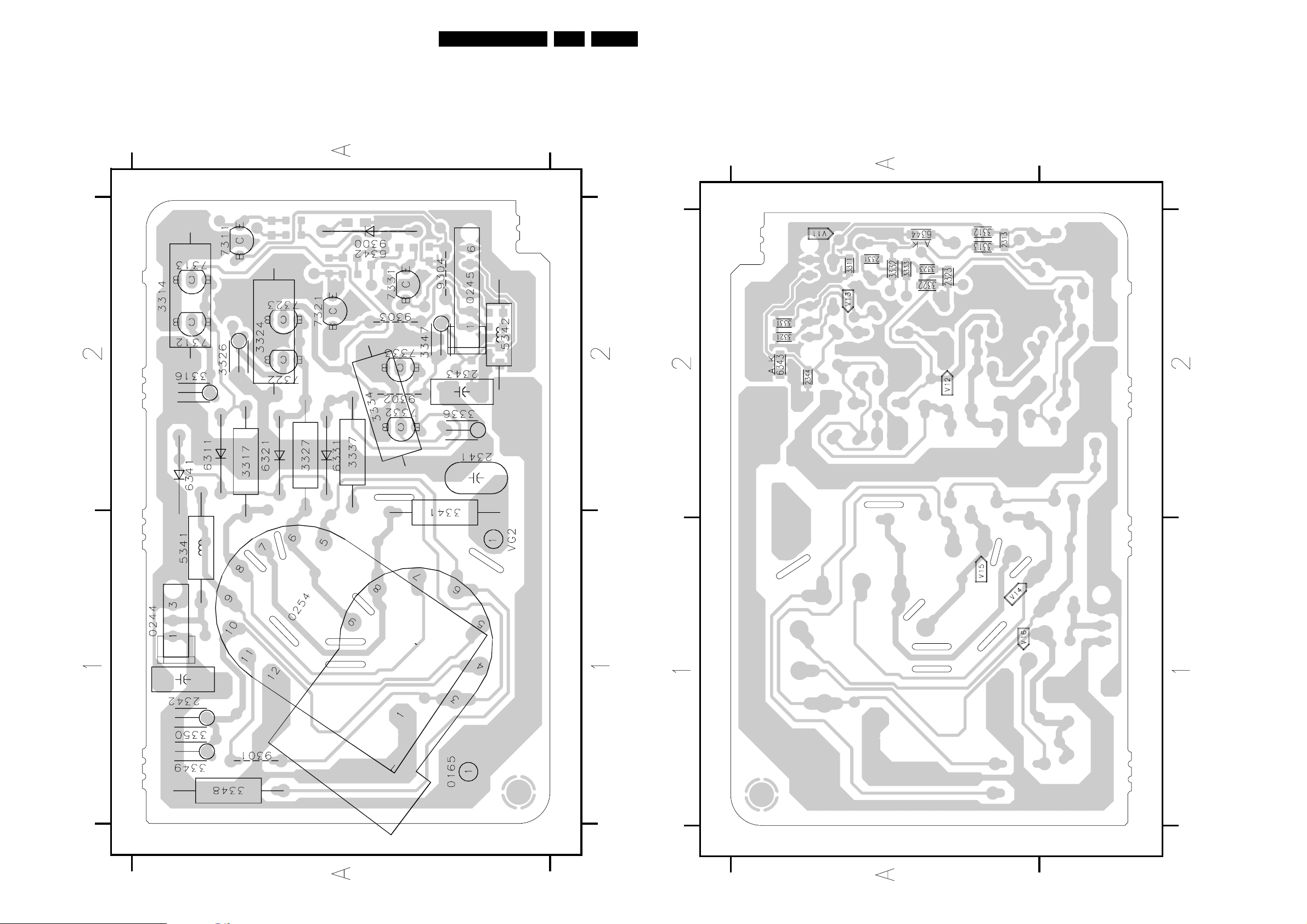
Schematics and PWB’s
50L01.2A 7.
Layout CRT Panel (Top View)
VG2 A1
0165 A1
0244 A1
0245 A2
0254 A1
1300 A1
2341 A2
2342 A1
2343 A2
3314 A2
3316 A2
3317 A2
3324 A2
3326 A2
3327 A2
3334 A2
3336 A2
3337 A2
3341 A1
3347 A2
3348 A1
3349 A1
3350 A1
5341 A1
5342 A2
6311 A2
6321 A2
6331 A2
6341 A2
6342 A2
7311 A2
7312 A2
7313 A2
7321 A2
7322 A2
7323 A2
7331 A2
7332 A2
7333 A2
9300 A2
9301 A1
9302 A2
9303 A2
9304 A2
140501
CL 16532051_015.eps
Layout CRT Panel (Bottom View)
2313 A2
2323 A2
2331 A2
2344 A2
3311 A2
3312 A2
3313 A2
3321 A2
3322 A2
3323 A2
3331 A2
3332 A2
3333 A2
6343 A2
6344 A2
140501
CL 16532051_016.eps
Page 71

Schematics and PWB’s
51L01.2A 7.
Side AV Panel
A
B
N.C
1234
SIDE AV
#
0252
1
2
3
4
0250-C
2175
330p
Ext1AudioR
0250-A
Layout Side AV Panel (Top View)
0250-A B1
0250-B C1
0250-C A1
0251 B4
0252 B1
0253 A4
A
B
0261 D4
1152 A2
1153 C2
1154 B2
2171 C3
2172 B3
2173 B2
2174 C2
2175 B1
3150 C3
3151 C3
3152 B3
3153 B3
3155 A3
5010 B3
6161 A3
9152 B2
9153 B3
9155 B3
0253
1
2
RES
3
1
2
3
#
0251
TO 0219 OF
2
3
1
8
9
7
*
9152
1154
1152
2173
*
*
9153
3153
RES
8K2
#
6161
*
BZX79-C6V8
10K
3152
2172
75R
3155
(FOR ESD)
330p
9155
5010
C
D
E
Ext1AudioL|Mono
* For 21" and below
47K
3150
1K
3151
47K
3152
1K
3153
For mono set w/out front cinch
9152
For stereo set w/out front cinch
9153
0250-B
3151
5
6
4
1153
*
8K2
RES
2174
3150
*
# For 25" and above
0251
For Chassis with Rear Scart
For Chassis with Rear Scart
0252
For Chassis with Rear Cinch
0261
BZX79-C6V8
6161
10K
2171
330p
3
4
5
6
1
2
#
0261
N.C
CL 16532020_055.eps
020401
C
D
E
CL 16532004_017.eps
210301
1234
Page 72

Schematics and PWB’s
52L01.2A 7.
Side AV Panel + Headphone
12345
SIDE AV PANEL & HEADPHONE
A
0252
1
2
3
4
AP/INDIA/LATAM
B
C
*
3156
3157
EUROPE
330R
330R
N.C
120R
120R
VIDEO IN
0250-C
RIGHT
0250-A
LEFT
0250-B
Layout Side AV Panel + Headphone (Top View)
0232 D4
0250-A B2
0250-B C2
0250-C A2
0251 B5
0252 B2
0253 A5
0254 D2
A
B
C
0255 D5
0261 C5
2171 C4
2172 B4
2173 B3
2174 C3
2176 E3
2177 E2
2178 E3
2179 D2
3150 C3
3151 C3
3152 B3
3153 B3
3155 A3
3156 D3
3157 E3
6161 A3
9153 B3
9155 B4
SG02 A3
SG03 C3
SG04 B3
SG06 E3
SG07 E3
0253
2
3
1
SG02SG04
6161
3155
BZX79-C6V8
75R
3
2
1
To 0219
of
A12
9153
RES
3153
8
9
7
5
6
4
SG03
2173
2174
8K2
330p
3151
8K2
330p
31523150
10K
10K
2172
2171
330p
330p
9155
(FOR ESD)
1
2
3
1
2
3
4
5
6
0251
0261
N.C
D
E
D
E
To 0246
of
HEADPHONE
0254
L-
L+
GND
R+
R-
1
0232
5
4
3
2
1
2179
100u
2177
100u
*
*
3156
330R
3157
330R
2178
2176
330p330p
SG07
SG06
6
5
4
2
3
7
8
9
0255
4
3
2
1
To
Speakers
L+
L-
To
Speakers
R-
R+
CL 16532020_056.eps
120401
12345
CL 16532004_016.eps
210301
 Loading...