

Philips ISP1103DH, ISP1103DB, ISP1103D Datasheet

ISP1103
Universal Serial Bus transceiver
Rev. 01 — 4 October 1999 Preliminary specification
1. General description
The ISP1103 is a single-chip generic Universal Serial Bus (USB) transceiver that is
fully compliant with the
USB Application Specific ICs (ASICs) and Programmable Logic Devices (PLDs) to
interface with the physical layer of the Universal Serial Bus. It supports transmitting
and receiving serial data at both full-speed (12 Mbit/s) and low-speed (1.5 Mbit/s)
data rates. It also supports the low-power single-ended input receiver interface in
‘suspend’ mode operation. The ISP1103 operates on a 3.3 V supply voltage.
The pin configuration conforms to the ‘Serial Interface Engine’ from the Universal
Serial Bus Implementers Forum (USB-IF). The ISP1103 allows for both the ‘USB-IF
Standard Data Interface’ and the ‘Philips Encoded Data Interface’. The ISP1103 is
fully pin compatible with the industry-standard Philips Semiconductors USB
transceiver PDIUSBP11A.
Universal Serial Bus Specification Rev. 1.1
. It allows 3.3 V
2. Features
■ Complies with
c
c
■ Supports full-speed (12 Mbit/s) and low-speed (1.5 Mbit/s) serial data rates
■ Slew-rate controlled differential data driver
■ Differential inputreceiver with wide common-mode range and very high data input
sensitivity
■ Stable RCV output during SE0 condition
■ Two single-ended receivers with hysteresis
■ Supports ‘Philips Encoded Data Interface’ and ‘USB-IF Standard Data Interface’
■ Low-power operation in ‘suspend’ mode
■ Operates on a 3.3 V supply voltage
■ Fully backward compatible with PDIUSBP11A
■ Compatible with VHDL ‘Serial Interface Engine’ from USB Implementers Forum
■ Higher than 8 kV ESD protection
■ Full industrial operating temperature range −40 to +85 °C
■ Available in SO14, SSOP14 and TSSOP14 packages.
Universal Serial Bus Specification Rev. 1.1
Philips Semiconductors
ISP1103
USB transceiver
3. Ordering information
Table 1: Ordering information
Type number Package
Name Description Version
ISP1103D SO14 plastic small outline package; 14 leads; body width 3.9 mm SOT108-1
ISP1103DB SSOP14 plastic shrink small outline package; 14 leads; body width 5.3 mm SOT337-1
ISP1103DH TSSOP14 plastic thin shrink small outline package; 14 leads; body width 4.4 mm SOT402-1
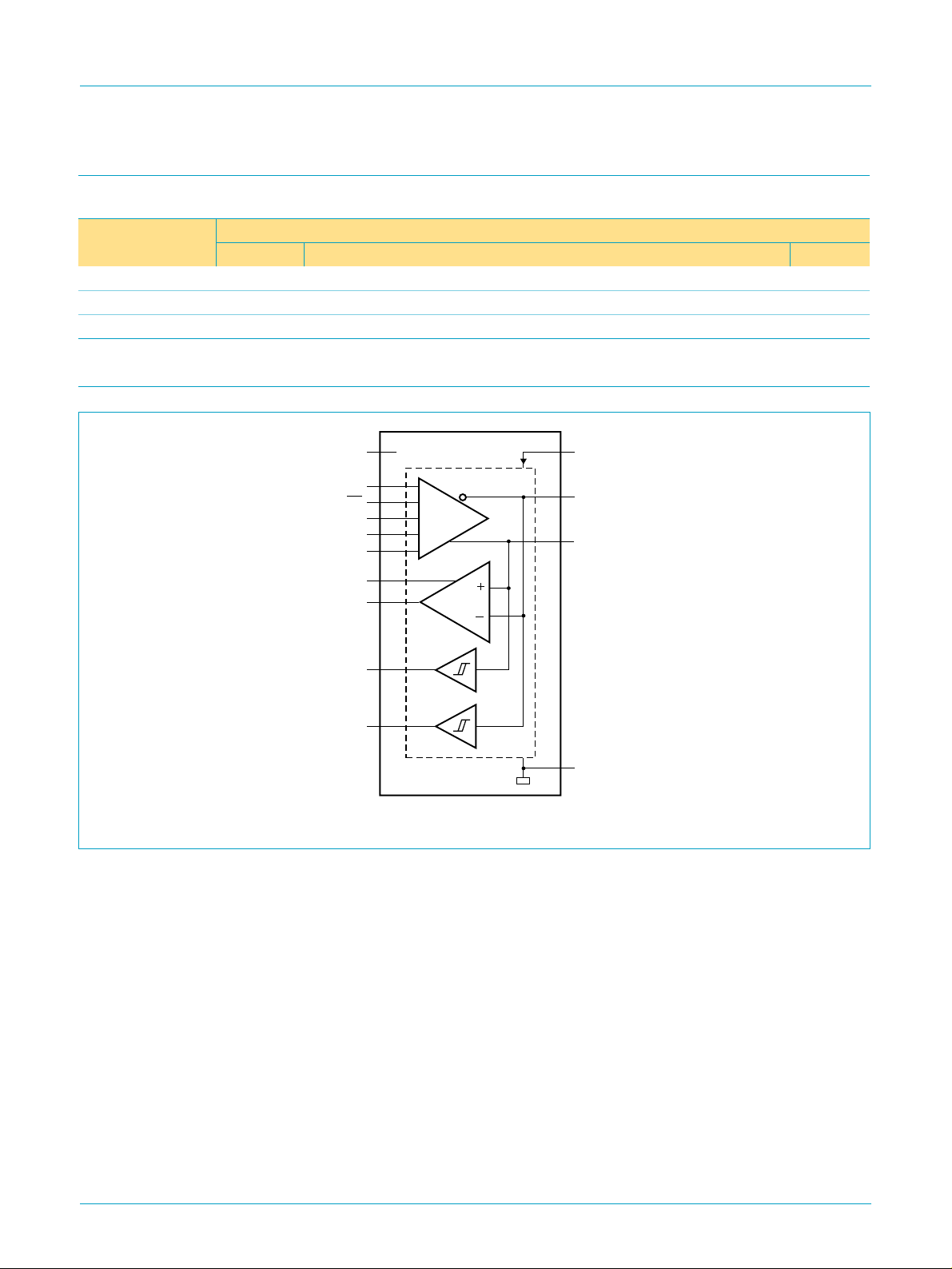
4. Functional diagram
Fig 1. Functional diagram.
handbook, halfpage
n.c.
MODE
OE
SPEED
VMO/FSE0
VPO/VO
SUSPND
RCV
VP
VM
8
1
2
9
13
12
6
3
4
5
ISP1103x
14
10
11
MBL094
V
CC(3.3)
D−
D+
7
GND
9397 750 06329
© Philips Electronics N.V. 1999. All rights reserved.
Preliminary specification Rev. 01 — 4 October 1999 2 of 17
Philips Semiconductors
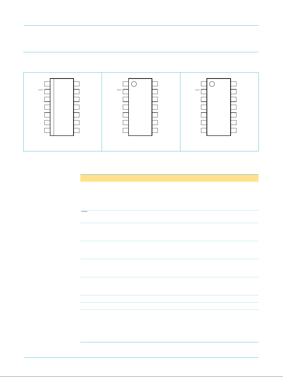
5. Pinning information
5.1 Pinning
ISP1103
USB transceiver
page
SUSPND
MODE
OE
RCV
VP
VM
GND
1
2
3
4
5
6
7
ISP1103D
MBL091
V
14
13
VMO/FSE0
12
VPO/VO
11
D+
10
D−
9
SPEED
n.c.
8
CC(3.3)
page
SUSPND
MODE
OE
RCV
VP
VM
GND
1
2
3
4
ISP1103DB
5
6
7
MBL092
V
14
13
VMO/FSE0
12
VPO/VO
11
D+
10
D−
9
SPEED
n.c.
8
CC(3.3)
page
SUSPND
MODE
OE
RCV
VP
VM
GND
1
2
3
4
ISP1103DH
5
6
7
MBL093
V
14
13
VMO/FSE0
12
VPO/VO
11
D+
10
D−
9
SPEED
n.c.
8
CC(3.3)
Fig 2. Pinning diagram SO14. Fig 3. Pinning diagram SSOP14. Fig 4. Pinning diagram TSSOP14.
5.2 Pin description
Table 2: Pin description
Symbol Pin Type Description
MODE 1 I driver interface selection input (Schmitt trigger):
LOW: Philips Encoded Data Interface (pins VO, FSE0)
HIGH: USB-IF Standard Data Interface (pins VPO, VMO);
pulled HIGH by an internal pull-up transistor, if left floating
OE 2 I output enable input (Schmitt trigger, active LOW); enables the
transceiver to transmit data on the bus
RCV 3 O differential data receiver output (CMOS level); driven HIGH
when input SUSPND is HIGH; the output state of RCV is
preserved and stable during an SE0 condition
VP 4 O single-ended D+ receiver output (CMOS level); used for
external detection of single-ended zero (SE0), error
conditions, speed of connected device
VM 5 O single-ended D− receiver output (CMOS level); used for
external detection of single-ended zero (SE0), error
conditions, speed of connected device
SUSPND 6 I suspend input (Schmitt trigger); a HIGH level enables
low-power state while the USB bus is inactive and drives
output RCV to a HIGH level
GND 7 - ground supply
n.c. 8 - not connected
SPEED 9 I speed selection input (Schmitt trigger); adjusts the slew rate
of differential data outputs D+ and D− according to the
transmission speed:
LOW: low-speed (1.5 Mbit/s)
HIGH: full-speed (12 Mbit/s)
9397 750 06329
© Philips Electronics N.V. 1999. All rights reserved.
Preliminary specification Rev. 01 — 4 October 1999 3 of 17

Philips Semiconductors
ISP1103
USB transceiver
Table 2: Pin description
Symbol Pin Type Description
D− 10 AI/O negative USB data bus connection (analog, differential); for
D+ 11 AI/O positive USB data bus connection (analog, differential); for
VPO/VO 12 I differential driver data input (Schmitt trigger); see Table 4
VMO/FSE0 13 I differential driver data input (Schmitt trigger); see Table 4
V
CC(3.3)
6. Functional description
6.1 Function selection
Table 3: Function table
SUSPND OE D+/D− RCV VP/VM Function
L L driving active active normal driving
L H receiving
H L driving inactive
H H high-Z
…continued
low-speed mode connect to pin V
full-speed mode connect to pin V
14 - supply voltage (3.0 to 3.6 V)
[1]
active active receiving
[2]
active driving during ‘suspend’
[1]
inactive
[2]
active low-power state
via a 1.5 kΩ resistor
CC(3.3)
via a 1.5 kΩ resistor
CC(3.3)
(differential receiver active)
(differential receiver inactive)
[1] Signal levels on D+/D− are determined by other USB devices and external pull-up/down resistors.
[2] In ‘suspend’ mode (SUSPND = H) the differential receiver is inactive and output RCV is always HIGH.
Out-of-suspend (‘K’) signalling is detected via the single-ended receivers VP and VM.
6.2 Operating functions
Table 4: Driving function (OE = L)
MODE Interface type VPO/VO VMO/FSE0 Data
L L differential logic 0
L
H
Philips Encoded
Data Interface
USB-IF Standard
Data Interface
Table 5: Receiving function (
D+/D− RCV VP VM
differential logic 0 L L H
differential logic 1 H H L
SE0 RCV* L L
OE=H)
L H SE0
H L differential logic 1
H H SE0
L L SE0
L H differential logic 0
H L differential logic 1
H H illegal data
[1] RCV* denotes the signal level on output RCV just before SE0 state occurs. This level is kept stable
during the SE0 period.
9397 750 06329
Preliminary specification Rev. 01 — 4 October 1999 4 of 17
© Philips Electronics N.V. 1999. All rights reserved.

Philips Semiconductors
ISP1103
USB transceiver
7. Limiting values
Table 6: Absolute maximum ratings
In accordance with the Absolute Maximum Rating System (IEC 60134).
Symbol Parameter Conditions Min Max Unit
V
CC(3.3)
V
I
I
latchup
V
esd
T
stg
P
tot
[1] Equivalent to discharging a 100 pF capacitor via a 1.5 kΩ resistor (Human Body Model).
Table 7: Recommended operating conditions
Symbol Parameter Conditions Min Max Unit
V
CC(3.3)
V
I
V
I(AI/O)
T
amb
supply voltage −0.5 +6.0 V
input voltage −0.5 VCC+ 0.5 V
latchup current VI< 0 or VI>V
electrostatic discharge voltage ILI<1µA
CC
- 200 mA
[1]
- ±8000 V
storage temperature −60 +150 °C
total power dissipation - <tbf> W
supply voltage 3.0 3.6 V
input voltage 0 5.5 V
input voltage on analog I/O pins
0 3.6 V
(D+/D−)
operating ambient temperature −40 +85 °C
8. Static characteristics
Table 8: Static characteristics: supply pins
VCC=V
Symbol Parameter Conditions Min Typ Max Unit
I
CC
I
CC(susp
; V
CC(3.3)
GND
=0V; T
=−40 to+85°C; unless otherwise specified.
amb
operating supply current - <tbf> - mA
) suspend supply current - - 10 µA
9397 750 06329
Preliminary specification Rev. 01 — 4 October 1999 5 of 17
© Philips Electronics N.V. 1999. All rights reserved.

Philips Semiconductors
ISP1103
USB transceiver
Table 9: Static characteristics: digital pins
VCC=V
Symbol Parameter Conditions Min Typ Max Unit
Schmitt trigger input levels
V
th(LH)
V
th(HL)
V
hys
Output levels
V
OL
V
OH
Leakage current
I
LI
; V
CC(3.3)
GND
=0V; T
positive-going threshold
=−40 to+85°C; unless otherwise specified.
amb
1.4 - 1.9 V
voltage
negative-going threshold
0.9 - 1.5 V
voltage
hysteresis voltage 0.4 - 0.7 V
LOW-level output voltage IOL= 3 mA - - 0.4 V
=20µA - - 0.1 V
I
OL
HIGH-level output voltage IOL= 3 mA 2.4 - - V
=20µAV
I
OL
CC(3.3)
−
--V
0.1
input leakage current - - ±1 µA
Table 10: Static characteristics: analog I/O pins (D+, D−)
VCC=V
CC(3.3)
; V
GND
=0V; T
=−40 to+85°C; unless otherwise specified.
amb
[1]
Symbol Parameter Conditions Min Typ Max Unit
Input levels
V
DI
V
CM
differential input sensitivity |V
differential common mode
− V
I(D+)
| 0.2 - - V
I(D−)
includes VDI range 0.8 - 2.5 V
voltage
V
IL
V
IH
V
hys
LOW-level input voltage - - 0.8 V
HIGH-level input voltage 2.0 - - V
hysteresis voltage 0.4 - 0.7 V
Output levels
V
OL
V
OH
LOW-level output voltage RL= 1.5 kΩ to V
CC(3.3)
HIGH-level output voltage RL=15kΩ to GND 2.8 - V
- - 0.3 V
CC(3.3)
V
Leakage current
I
LZ
OFF-state leakage current - - ±10 µA
Capacitance
C
IN
transceiver capacitance pin to GND - - 20 pF
Resistance
Z
DRV
Z
INP
driver output impedance
input impedance 10 - - MΩ
[2]
steady-state drive 28 - 44 Ω
Termination
V
TERM
termination voltage
[3]
for
upstream port pull-up (R
PU
)
3.0
[4]
- 3.6 V
[1] D+ is the USB positive data pin; D− is the USB negative data pin.
[2] Includes external resistors of 22 Ω±1% or 24Ω±1% on both D+ and D−.
[3] This voltage is available at pin V
[4] In ‘suspend’ mode the minimum voltage is 2.9 V.
9397 750 06329
Preliminary specification Rev. 01 — 4 October 1999 6 of 17
CC(3.3)
.
© Philips Electronics N.V. 1999. All rights reserved.
 Loading...