

Philips IRF840 Datasheet
Philips Semiconductors Product specification
PowerMOS transistor IRF840
Avalanche energy rated
FEATURES SYMBOL QUICK REFERENCE DATA
• Repetitive Avalanche Rated
• Fast switching V
d
= 500 V
DSS
• High thermal cycling performance
• Low thermal resistance I
g
s
R
DS(ON)
= 8.5 A
D
≤ 0.85 Ω
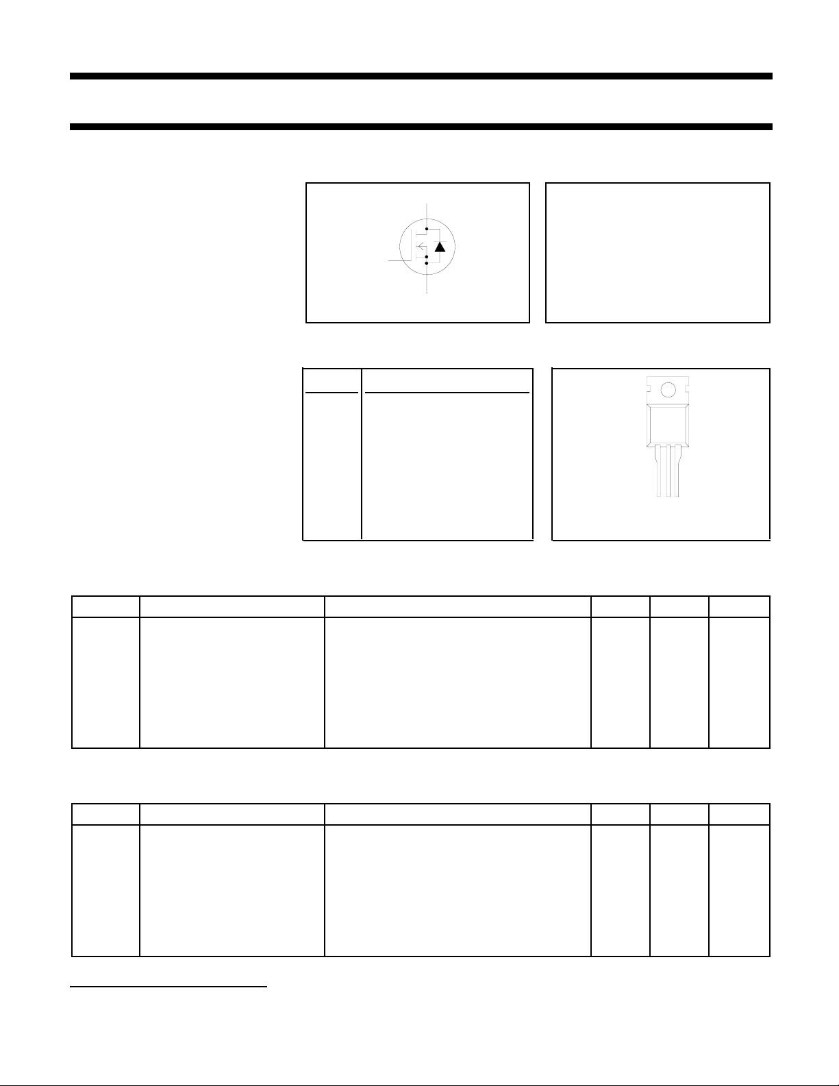
GENERAL DESCRIPTION PINNING SOT78 (TO220AB)
N-channel, enhancement mode PIN DESCRIPTION
field-effect power transistor,
intendedforuse in off-line switched 1 gate
mode power supplies, T.V. and
computer monitor power supplies, 2 drain
d.c.tod.c.converters,motorcontrol
circuits and general purpose 3 source
switching applications.
tab drain
The IRF840 is supplied in the
SOT78 (TO220AB) conventional
leaded package.
tab
123
LIMITING VALUES
Limiting values in accordance with the Absolute Maximum System (IEC 134)
SYMBOL PARAMETER CONDITIONS MIN. MAX. UNIT
V
DSS
V
DGR
V
GS
I
D
I
DM
P
D
Tj, T
Drain-source voltage Tj = 25 ˚C to 150˚C - 500 V
Drain-gate voltage Tj = 25 ˚C to 150˚C; RGS = 20 kΩ - 500 V
Gate-source voltage - ± 30 V
Continuous drain current Tmb = 25 ˚C; VGS = 10 V - 8.5 A
Tmb = 100 ˚C; VGS = 10 V - 5.4 A
Pulsed drain current Tmb = 25 ˚C - 34 A
Total dissipation Tmb = 25 ˚C - 147 W
Operating junction and - 55 150 ˚C
stg
storage temperature range
AVALANCHE ENERGY LIMITING VALUES
Limiting values in accordance with the Absolute Maximum System (IEC 134)
SYMBOL PARAMETER CONDITIONS MIN. MAX. UNIT
E
AS
E
AR
IAS, I
1 pulse width and repetition rate limited by Tj max.
March 1999 1 Rev 1.000
Non-repetitive avalanche Unclamped inductive load, IAS = 7.4 A; - 531 mJ
energy tp = 0.22 ms; Tj prior to avalanche = 25˚C;
VDD ≤ 50 V; RGS = 50 Ω; VGS = 10 V; refer
to fig:17
Repetitive avalanche energy1IAR = 8.5 A; tp = 2.5 µs; Tj prior to - 13 mJ
avalanche = 25˚C; RGS = 50 Ω; VGS = 10 V;
refer to fig:18
Repetitive and non-repetitive - 8.5 A
AR
avalanche current

Philips Semiconductors Product specification
PowerMOS transistor IRF840
Avalanche energy rated
THERMAL RESISTANCES
SYMBOL PARAMETER CONDITIONS MIN. TYP. MAX. UNIT
R
th j-mb
R
th j-a
ELECTRICAL CHARACTERISTICS
Tj = 25 ˚C unless otherwise specified
SYMBOL PARAMETER CONDITIONS MIN. TYP. MAX. UNIT
V
(BR)DSS
∆V
(BR)DSS
∆T
j
R
DS(ON)
V
GS(TO)
g
fs
I
DSS
I
GSS
Q
g(tot)
Q
gs
Q
gd
t
d(on)
t
r
t
d(off)
t
f
L
d
L
d
L
s
C
iss
C
oss
C
rss
Thermal resistance junction - - 0.85 K/W
to mounting base
Thermal resistance junction in free air - 60 - K/W
to ambient
Drain-source breakdown VGS = 0 V; ID = 0.25 mA 500 - - V
voltage
/ Drain-source breakdown VDS = VGS; ID = 0.25 mA - 0.1 - %/K
voltage temperature
coefficient
Drain-source on resistance VGS = 10 V; ID = 4.8 A - 0.6 0.85 Ω
Gate threshold voltage VDS = VGS; ID = 0.25 mA 2.0 3.0 4.0 V
Forward transconductance VDS = 30 V; ID = 4.8 A 3.5 6 - S
Drain-source leakage current VDS = 500 V; VGS = 0 V - 1 25 µA
VDS = 400 V; VGS = 0 V; Tj = 125 ˚C - 40 250 µA
Gate-source leakage current VGS = ±30 V; VDS = 0 V - 10 200 nA
Total gate charge ID = 8.5 A; V
Gate-source charge - 5.5 7 nC
= 400 V; VGS = 10 V - 55 80 nC
DD
Gate-drain (Miller) charge - 30 45 nC
Turn-on delay time VDD = 250 V; RD = 30 Ω; - 18 - ns
Turn-on rise time RG = 9.1 Ω -37-ns
Turn-off delay time - 80 - ns
Turn-off fall time - 36 - ns
Internal drain inductance Measured from tab to centre of die - 3.5 - nH
Internal drain inductance Measured from drain lead to centre of die - 4.5 - nH
Internal source inductance Measured from source lead to source - 7.5 - nH
bond pad
Input capacitance VGS = 0 V; VDS = 25 V; f = 1 MHz - 960 - pF
Output capacitance - 140 - pF
Feedback capacitance - 80 - pF
SOURCE-DRAIN DIODE RATINGS AND CHARACTERISTICS
Tj = 25 ˚C unless otherwise specified
SYMBOL PARAMETER CONDITIONS MIN. TYP. MAX. UNIT
I
S
I
SM
V
SD
t
rr
Q
rr
March 1999 2 Rev 1.000
Continuous source current Tmb = 25˚C - - 8.5 A
(body diode)
Pulsed source current (body Tmb = 25˚C - - 34 A
diode)
Diode forward voltage IS = 8.5 A; VGS = 0 V - - 1.2 V
Reverse recovery time IS = 8.5 A; VGS = 0 V; dI/dt = 100 A/µs - 440 - ns
Reverse recovery charge - 6.4 - µC
Philips Semiconductors Product specification
PowerMOS transistor IRF840
Avalanche energy rated
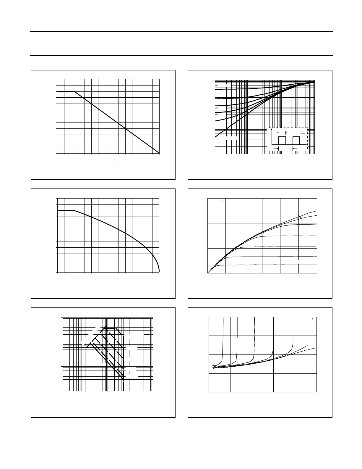
PD%
120
110
100
90
80
70
60
50
40
30
20
10
0
0 20 40 60 80 100 120 140
Normalised Power Derating
Tmb / C
Fig.1. Normalised power dissipation.
PD% = 100⋅PD/P
ID%
120
110
100
90
80
70
60
50
40
30
20
10
0
0 20 40 60 80 100 120 140
Tmb / C
= f(Tmb)
D 25 ˚C
Normalised Current Derating
Fig.2. Normalised continuous drain current.
ID% = 100⋅ID/I
= f(Tmb); conditions: VGS ≥ 10 V
D 25 ˚C
Zth j-mb, Transient thermal impedance (K/W)
1
D = 0.5
0.2
0.1
0.1
0.05
0.02
0.01
single pulse
0.001
1us
10us 100us
1ms 1s
tp, pulse width (s)
P
D
10ms 100ms
PHP6N60
t
D =
p
T
t
t
p
T
Fig.4. Transient thermal impedance.
Z
= f(t); parameter D = tp/T
th j-mb
ID, Drain current (Amps)
30
Tj = 25 C
25
20
15
10
5
0
0 5 10 15 20 25 30
VDS, Drain-Source voltage (Volts)
PHP8N50
7 V
VGS = 4.5 V
Fig.5. Typical output characteristics
ID = f(VDS); parameter V
GS
10 V
6.5 V
6 V
5.5 V
5 V
.
ID / A
100
10
1
0.1
1 10 100 1000
RDS(ON) = VDS/ID
DC
VDS / V
BUK457-500B
tp = 10 us
100 us
1 ms
10 ms
100 ms
Fig.3. Safe operating area. Tmb = 25 ˚C
ID & IDM = f(VDS); IDM single pulse; parameter t
RDS(on), Drain-Source on resistance (Ohms)
2
4.5 V VGS = 6 V
1.5
1
0.5
0
0 5 10 15 20 25
5 V 5.5 V
ID, Drain current (Amps)
Fig.6. Typical on-state resistance
R
p
= f(ID); parameter V
DS(ON)
6.5 V
GS
PHP8N50
Tj = 25 C
7 V
10 V
.
March 1999 3 Rev 1.000
 Loading...