

Philips FW C100 C37 Service Manual

TRAINING INFORMATION
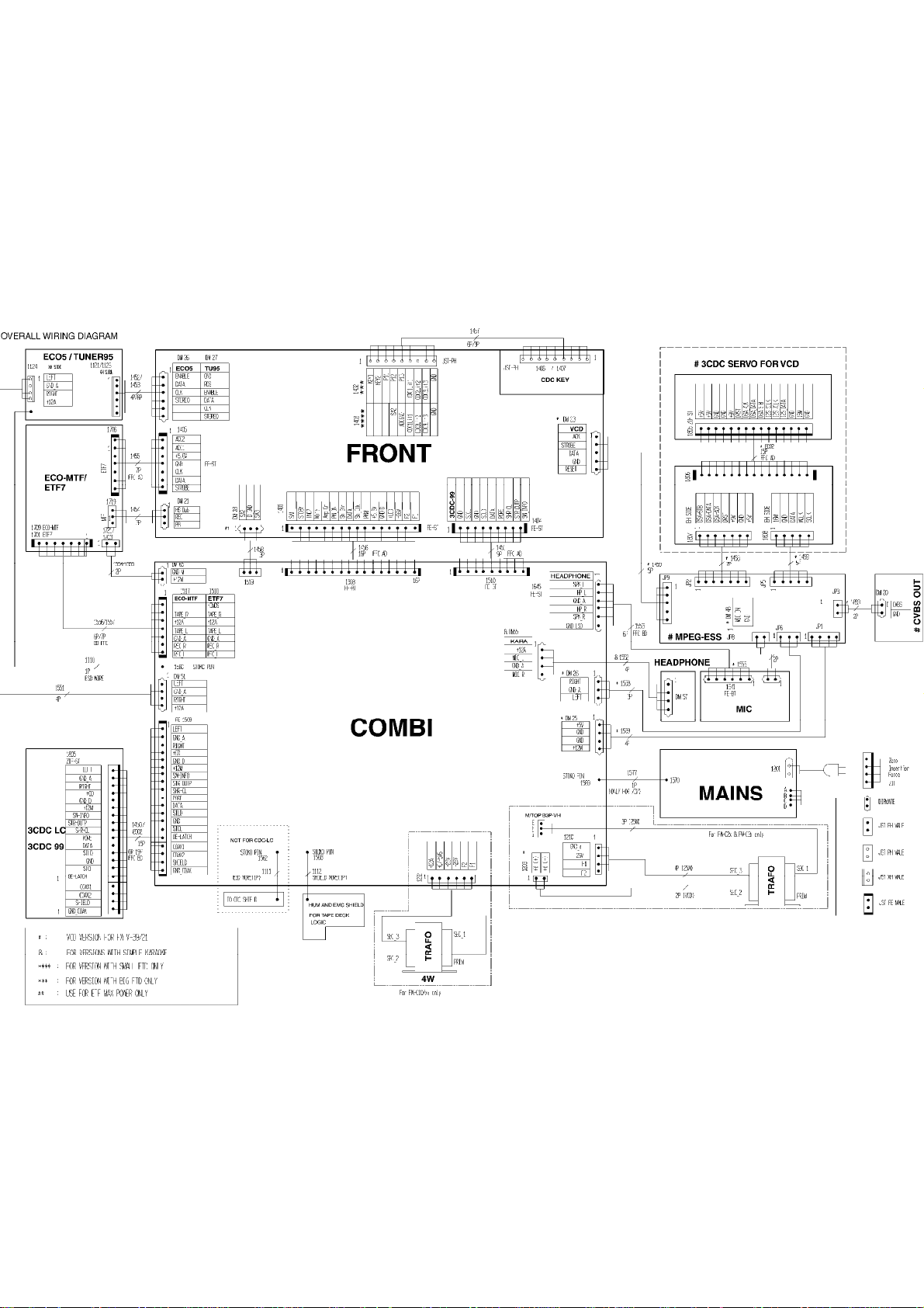
DISPLAY OVERALL BLOCK DIAGRAM
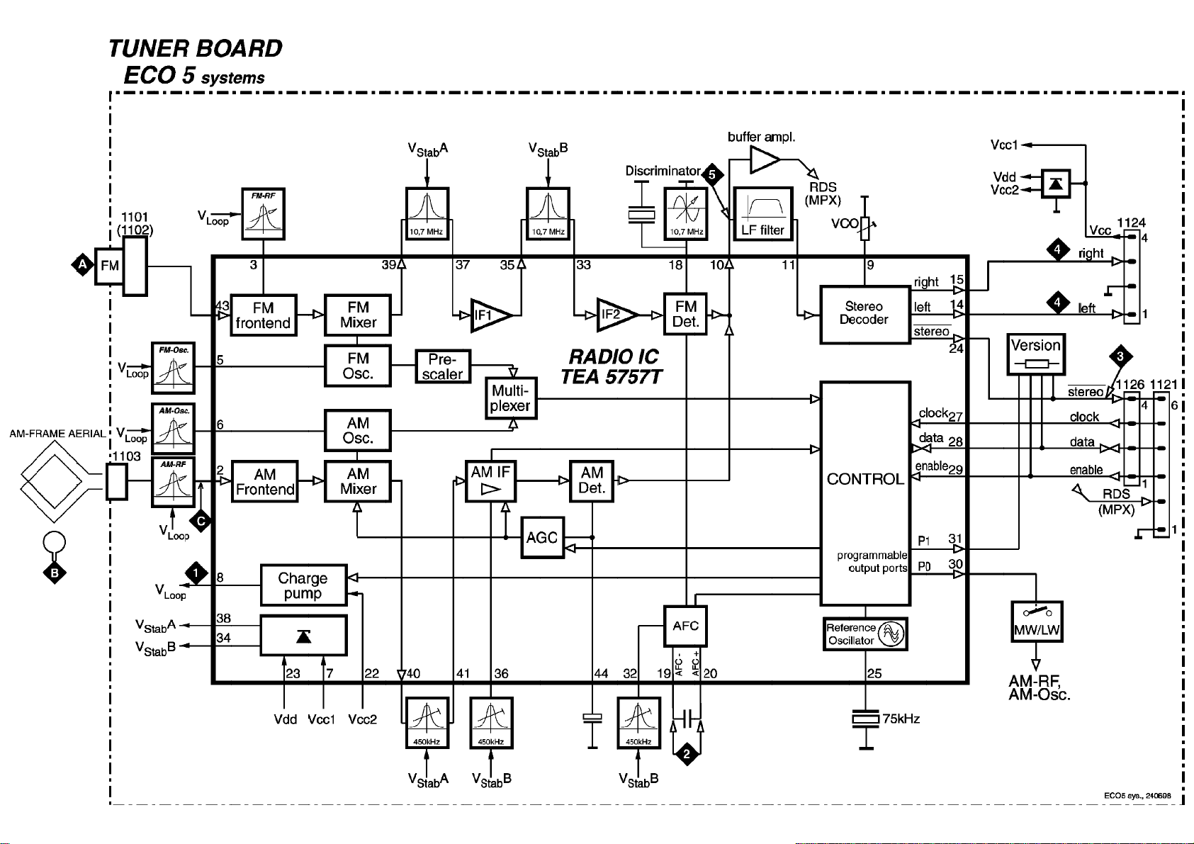
DISPLAY EC05 TUNER BLOCK DIAGRAM
DISPLAY 3CDC-LC BLOCK DIAGRAM
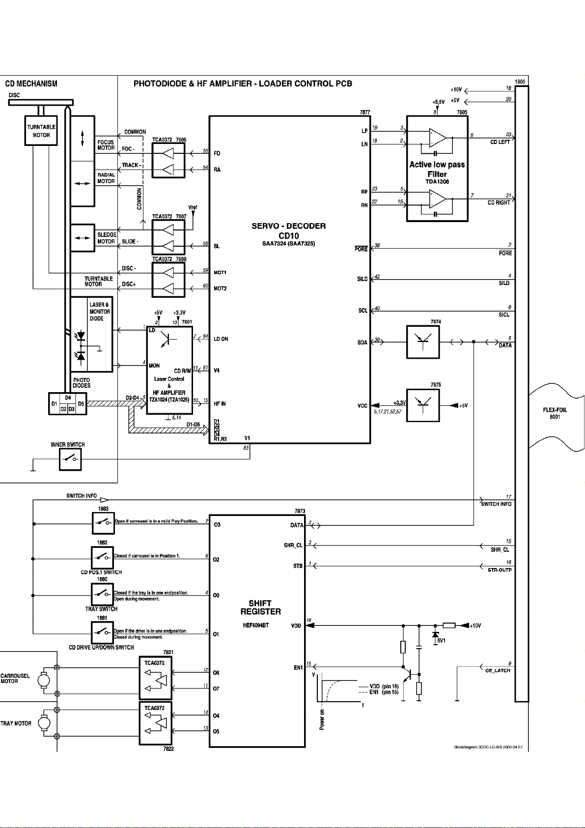
DISPLAY 3CDC-LC-MB BLOCK DIAGRAM
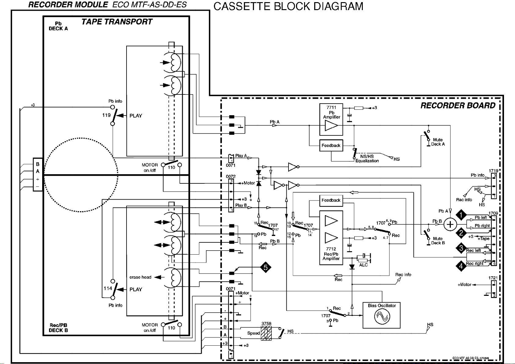
DISPLAY CASSETTE BLOCK DIAGRAM
Brief Introduction of the Combi Board
A. TRANSFORMER PRIMARY PART
The Transfor mer Primary Circuit provides connections for AC mains supply and
primar y wires of transformer.
B. POW ER SUPPLY PART
Power Supply Circ uit consists of recti fiers, c apacitive filt ers, and voltage r egulators.
Regulated v oltages include + 5V6, +LED, + 12A, +12M, -33V, PW DN. The +C supply
to the power amplifier is not regulated. F1-F2 is the ac supply voltage to the FTD
Display filament.
C. SOURCE SELECT AND AMPLIFIER PA RT
a) SHIFT RE G I S TER (AF CONTRO L)
The shift register IC 7402 (HEF 4094BP) deli vers comm ands from the uP to cont rol
the AF functions which include source selection (A0 and A1 control lines), DSC
modes, DBB, IS and CD_ON (via +CD). Other control lines, such as MUTE,
AMPON, STB Y and P WM, are c oming direct ly from the uP on the Front B oar d.
b) SOURCE SELECTION
One of the four sources, namely AUX., T APE, T UNER, or CD, can be selected v ia
A0 and A1 lines which control IC7501 (HEF4052BP). Karaoke mic. mixing is
connected to the selected source before the signal is amplified with a buffer
amplif ier (Tr 7503 and 7504). The source signal i s then split into recordi ng path
(for recordi ng on t ape) and main signal path (to the PWM volume control).
c) PWM VOLUME CONT ROL
The discrete v olum e control makes use of four transistors: 7505, 7506, 7507, and
7508 (ON4986 or paired BC557B) and PWM control signal from uP. For good
performanc e, transistors for t he left and right channels should be pai red for gain
characteristics.
d) SOUND FEAT URE S

Sound features include the DBB, IS, and DSC modes. The sound features are
realized with hex-inverter IC7530 (HEF4069UBD) as analog buffer/amplif ier and
transistors as electronic switches cont r olled by the shif t registers (AF control).
e) POWER AMPLIFIER
IC7391 (AN7124) is used as a power amplifier.
f) CD ON CO NTROL
This circuit switches on the +CD supply (derived f rom +12A) to CD servo control,
HF circuit, and the laser light pen on the CD Module during t he CD mode only.
g) MATRIX SURROUND O UTPUT
The mat rix surround feat ure i s provided onboard. T his feature is optional on
certain ty pe versions.
D. KARAOKE PART
a) SIMPLE KARAOKE
This is a one-m ic. mono amplif ier using discrete components. It has level control
using a rotary potenti ometer. Thi s feature is av ailable for som e versions only.
E. HEADPHONE PART
a) HEADPHONE OUTPUT
The headphone output is derived from the power amplifier output after the
attenuation resistors, which ar e tailored to del iver 25mW out put power into a 32
ohm headphone.
F. CDC KEY PART
CDC key buttons and LEDs are provided on this board.
Front Board Application
A53920 FW-C200/12/21/21M/33
A53930 FW-C220/22/34
A53950 FW-C100/21/21M/22/30/33/34/37
A53970 FW-C250/37
A53980 FW-C250/18/19/21
A53990 FW-C280/22/34
A54000 FW-C290/18/19/21
A54340 FW-C200/30
FEATURES: A53920 A53930 A53950 A53970 A53980 A53990 A54000 A54340
RDS - x - - - x - Rotary Encoder x x - x x x x x
Jog Encoder - - - x x x x Spectrum Analyzer - - - - - x x Biplaner LED x x - x x x x x
Small FTD x x x x x - - x
Large FTD - - - - - x x NTC - - - - x - x -

LED Control x x - x x x x x
Variations Table for Front Board
ITEM NO. A53920 A53930 A53950 A53970 A53980 A53990 A54000 A54340
DM21 - - x x x - - DM23 - - - - - - - DM26 x - x x x - x x
DM27 - x - - - x - DM29 - - - - x - x 1402 - - - - - x x 1403 x x x x x - - x
1404 x x x x x x x x
1405 x x - - - x x x
1418 - - - - - x x x
1419 - - - - - x x x
1420 - - - - - x x x
1421 x x - - - x x x
1423 x x - - - x x x
1425 - x - - - x - 1426 x x - - - x x x
1427 - x - - - x - 1428 - - x - - - - 1429 - - x - - - - 1430 x x x - - - - 2417 220uF 220uF - 220uF 220uF 220uF 220uF 220uF
2421 22uF 22uF 2,2uF 22uF 22uF 22uF 22uF 22uF
2432 - 100pF - - - 100pF - 2433 - 47pF - - - 47pF - 2462 220nF 220nF - 220nF 220nF 220nF 220nF 220nF
3407 - - - - - 1k 1k 1k
3458 - - - - - 1k 1k 1k
3460 - - - - - 1k 1k 1k
3465 1k 1k - 1k 1k 1k 1k 1k
3471 4R7 4R7 4R7 4R7 4R7 1R 1R 1R
3479 1k 1k - 1k 1k 1k 1k 1k
3483 4R7 4R7 4R7 4R7 4R7 1R 1R 1R
3516 - - 330R - - - - 3518 - - - - - 330R 330R 3524 1k 1k - - - 1k 1k 1k
3539 10k - 10k 10k 10k - 10k 10k
3541 - 1k - - - 1k - 3546 10k - 10k 10k 10k - 10k 10k
3555 10k 10k 10k 10k 10k - - 10k
3575 10k 10k 10k 10k 10k - - 10k
3576 10k 10k 10k 10k 10k - - 10k
3577 - - - - - 12k 12k 3578 - - - - - 5k6 5k6 3586 - - - - - 1k 1k 3588 - - 10k - - - - 3600 5k6 5k6 5k6 5k6 5k6 - - 3602 - - 10k 10k 10k - - 3603 10k 10k 6k8 10k 10k 10k 10k 10k
3613 12k 12k 47k 12k 12k 12k 12k 12k

3616 - - - - 1k - 1k 3617 10k 10k 10k 10k - 10k - 10k
4400 x x x - - - - x
4407 x x - x x - - x
4410 x x x x - x - x
4412 - - - - - x x 4413 - - x - - - - 4417 x x - - - - - x
4436 x x - - - - - x
4588 - - x - - - - 6401 - - - x x x x 6402 - - - x x x x 6404 - - - x x x x 6405 - - - - - x x 6420 - - - - - x x 6422 - - x - - - - 6423 x - - - x - x 6424 - - - x x - - 6428 x x - x x x x x
6433 - - - x x - - 6445 x x - - - - - x
6446 x x - - - - - x
6447 x x - x x - - x
9475 x x x x x - - x
9488 - - - x x x x 9520 - - - x x x x 9523 x x x x x - - x
x = Item in use.


FWC100C37(1975) - OVERALL WIRING DIAGRAM Page: 1 of 30
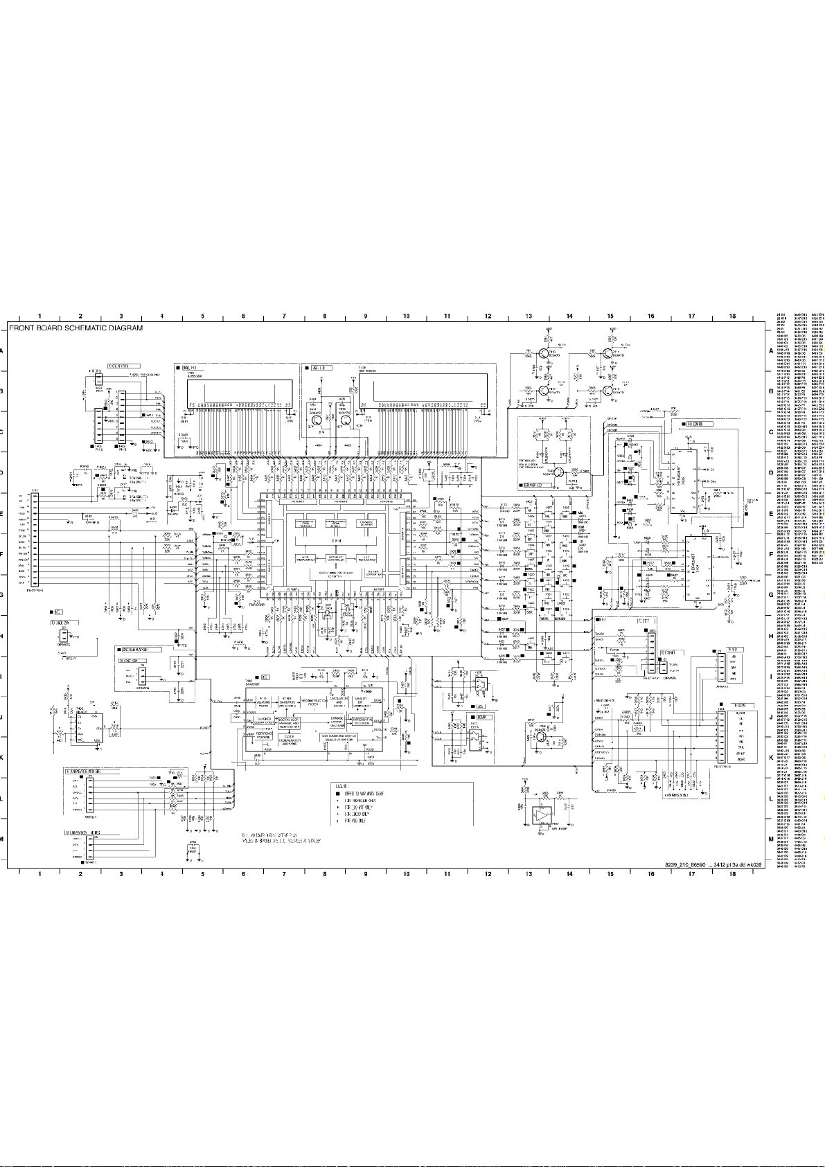
FWC100C37(1975) - FRONT BOARD SCHEMATIC DIAGRAM Page: 2 of 30
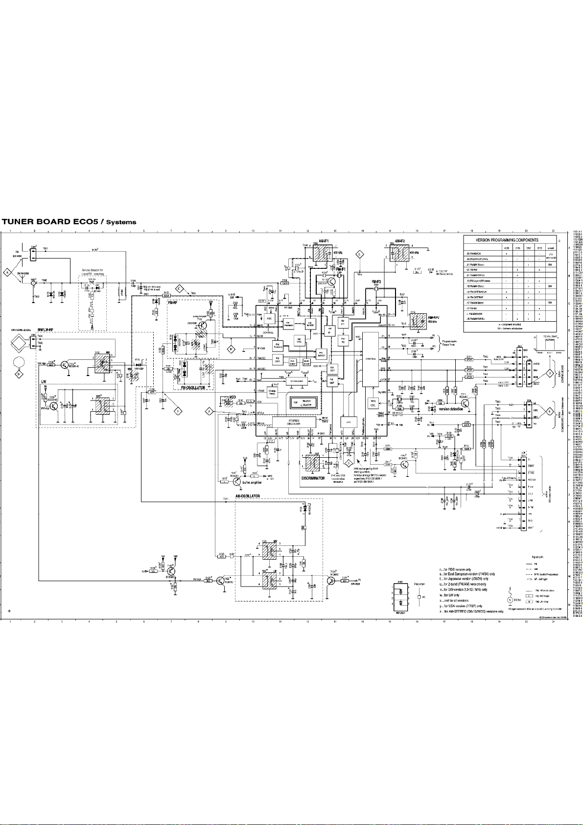
FWC100C37(1975) - EC05 TUNER SCHEMATIC DIAGRAM Page: 3 of 30

FWC100C37(1975) - CASSETTE SCHEMATIC DIAGRAM Page: 4 of 30
FWC100C37(1975) - 3CDC-LC CD SCHEMATIC DIAGRAM 1 Page: 5 of 30
FWC100C37(1975) - 3CDC-LC CD SCHEMATIC DIAGRAM 2 Page: 6 of 30
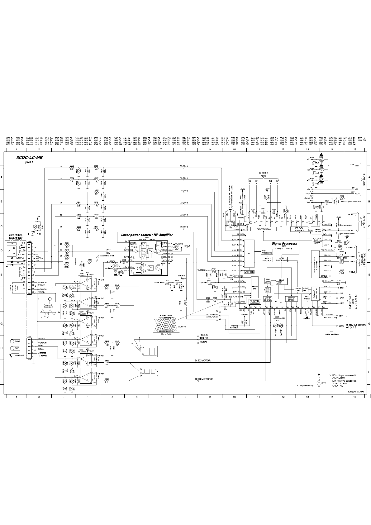
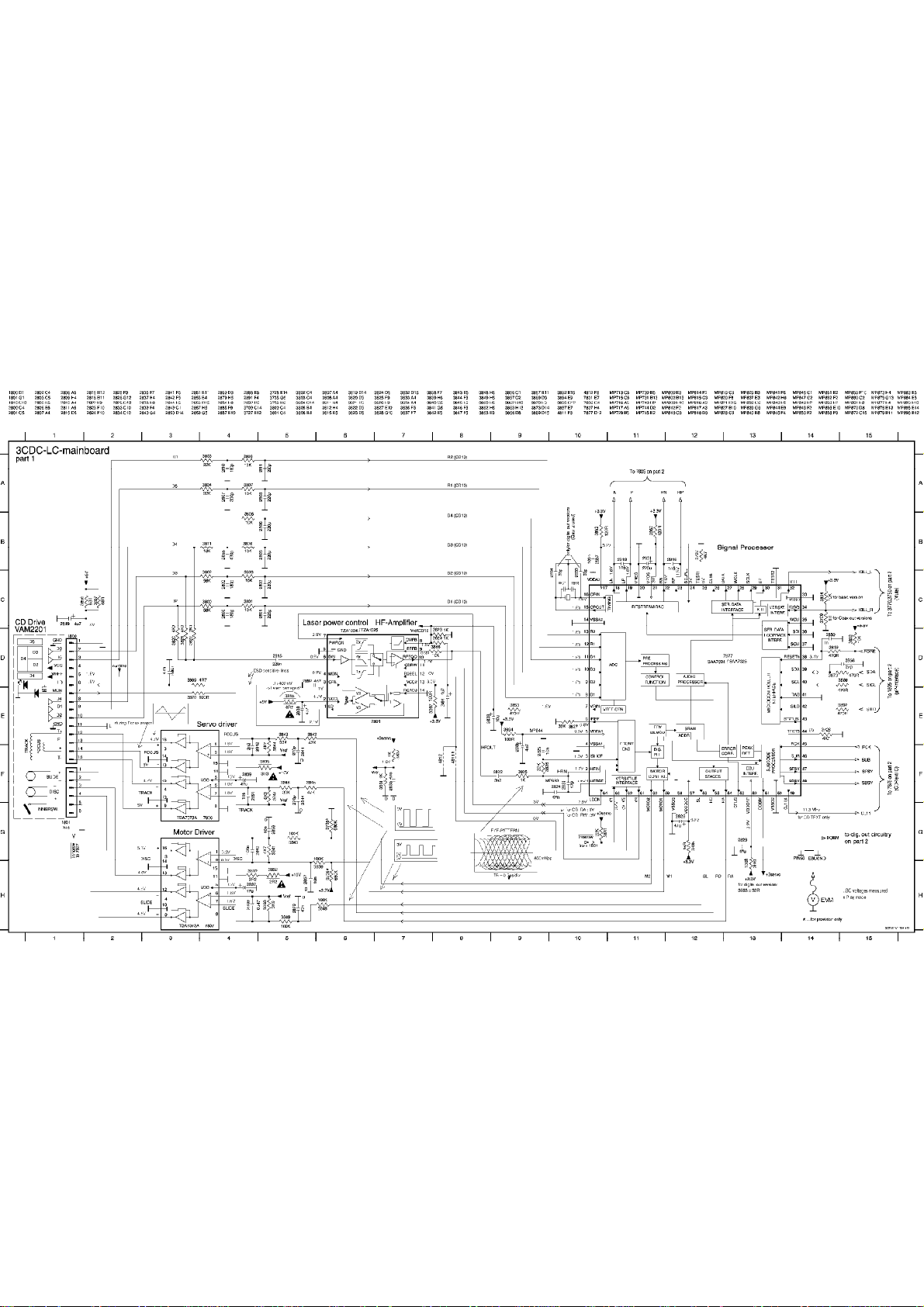
FWC100C37(1975) - 3CDC-LC-MB SCHEMATIC DIAGRAM 1 Page: 7 of 30

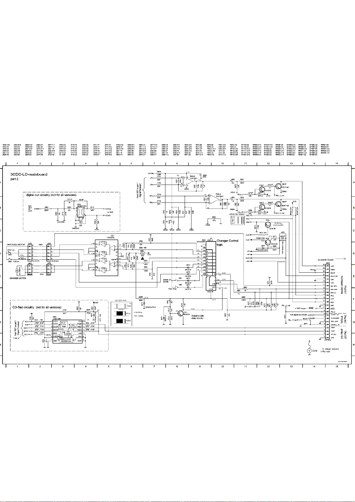
FWC100C37(1975) - 3CDC-LC-MB CD SCHEMATIC DIAGRAM 2 Page: 8 of 30
 Loading...