

Philips DFR-9000, DRF-9000 Service manual
DFR9000
all versions
© 3103 785 25290
Published by PW 0510 Service Audio Printed in The Netherlands Subject to modification
Version 1.0
Digital Surround Receiver
TABLE OF CONTENTS
©
Copyright 2005 Philips Consumer Electronics B.V. Eindhoven, The Netherlands
All rights reserved. No part of this publication may be reproduced, stored in a retrieval
system or transmitted, in any form or by any means, electronic, mechanical, photocopying,
or otherwise without the prior permission of Philips.
Technical Specification......................................................1-1
Connections & Controls.....................................................1-2
Accessories .......................................................................1-4
Safety & Warnings.............................................................2-1
Firmware Upgrade.............................................................2-2
Service Test Program........................................................2-3
Standby-LED Blinking State..............................................2-9
Location of Printed Boards................................................3-1
Dismantling........................................................................3-1
Block & Wiring Diagram.....................................................3-2
Circuit Diagrams & Printed Boards
Standby Power Supply..................................................4-1
Power Supply AC6750..................................................5-1
Front Control .................................................................6-1
Digital I/O ......................................................................7-1
Video Processing Board................................................8-1
Video I/O.......................................................................9-1
Front Left.....................................................................10-1
Front I/O......................................................................11-1
Front Keys...................................................................12-1
Front Right ..................................................................13-1
Audio Signal Processing Board...................................14-1
UCD Amplifier .............................................................15-1
Speaker Terminal........................................................16-1
DAB Interface..............................................................17-1
Exploded View.................................................................18-1
Partslist............................................................................18-2
Revision list .....................................................................18-2

1-1
TECHNICAL SPECIFICATION
General
Dimensions : 435 x 100 x 370mm
Net weight : 7.0kg
Power Supply /22S : 230V ±10%, 50Hz
Power consumption Standby : ≤0.5W
DAB Tuner
Tuning range : 174-240MHz (Band III)
1452-1492MHz (L)
AM Tuner
Tuning range /22S : 531-1602kHz, 9kHz grid
Tuning range /37 : 530-1700kHz, 10kHz grid
IF : 450kHz
Sensitivity (26dB S/N) : ≤3250µV/m (2000µV/m)
Distortion (rf=1mV, m=80%) : ≤5% (4% typ.)
FM Tuner
Tuning range /22S : 87.5-108MHz, 50kHz grid
Tuning range /37 : 87.5-108MHz, 100kHz grid
IF : 10.7MHz
Sensitivity (26dB S/N) : ≤22dBf (15dBf typ.)
-3dB limiting point : ≤23.5dBf (10dBf typ.)
Distortion (rf=1mV, m=80%) : ≤3% (0.23% typ.)
Crosstalk (rf=1mV, ∆f=75kHz) : ≤-26dB (-48dB typ.)
Video performance – Composite Video
Signal level : 1Vpp (75Ω)
Frequency response : 0-6MHz
S/N ratio : >50dB
Video performance – S-Video
Signal level Y : 1Vpp (75Ω)
Signal level C : 0.286Vpp (75Ω)
Frequency response : 0-6.5MHz
S/N ratio : >65dB
Video performance – Component Video / RGB
Signal level Y : 1Vpp (75Ω)
Signal level PB/CB, PR/CR : 0,7Vpp (75Ω)
Signal level R/G/B : 0,7Vpp (75Ω)
Frequency response : 0-7MHz
Frequency resp. progressive : 0-16MHz
S/N ratio : >70dB
Video input resolutions/formats
PAL 576i (720 x 576i)
PAL progressive 576p (720 x 576p, downscaled to 576i)
NTSC 480i (720 x 480i)
NTSC progressive 480p (720 x 480p, downscaled to 480i)
Video output resolutions/formats
PAL input 50Hz (TV) : 576i (720 x 576i)
576p (720 x 576p)
720p (1280 x 720p)
1080i (1920 x 1080i)
NTSC input 60Hz (TV) : 480i (720 x 480i)
480p (720 x 480p)
720p (1280 x 720p)
1080i (1920 x 1080i)
Digital video input/output
PAL input 50Hz (TV) : 576i (720 x 576i)
576p (720 x 576p)
720p (1280 x 720p)
1080i (1920 x 1080i)
NTSC input 60Hz (TV) : 480i (720 x 480i)
480p (720 x 480p)
720p (1280 x 720p)
1080i (1920 x 1080i)
PC input 60Hz : VGA (640 x 480p)
SVGA (800 x 600p)
XGA (1024 x 768p)
SXGA (1280 x 1024p)
Audio Line-in
Input sensitivity : 0.2-2.8Vrms
Input impedance : 22kΩ
Audio Line/Rec Out
Output voltage : 1.6Vrms
Outut impedance : 1kΩ
Frequency response : 5Hz-100kHz
S/N ratio : 110dBA typ.
THD (1kHz, 1W) : ≤0.0016%
Power amplifier
Output power (1kHz, THD=1%): 2 x 110W RMS into 4Ω
6 x 65W RMS into 4Ω
Frequency response (1W) : 5Hz-45kHz
S/N ratio : 105dBA typ.
THD (1kHz, 1W) : ≤0.065%
ADC/DAC
Resolution : 24bits/96kHz
Digital In/Out
Coaxial input : 0.2Vpp, 75Ω
Coaxial output : 0.5Vpp, 75Ω
Supported multichannel formats
Dolby ProLogic IIx, Dolby Digital, Dolby Digital EX, DTS,
DTS 96/24, DTS ES Matrix, DTS ES Discret, DTS NEO:6
1-2
CONNECTIONS & CONTROLS
Front View
soP noitcnuF skrameR
1NO-YBDNATS
derpusthgil)nottubybdnats/rewoPehtnirotacidni(DELnO/ybdnatS.ybdnatsotdnanotesehtsehctiwS
.ffodehctiwssitesehtnehw
2NWOD/PU
.edomreifilpmanisecruosdetcennocsuoiravehtstceleS
.unemehtninoitceridnwoddnapunisetagivaN-
.edomBADdnarenuTninoitatsgnitsacdaorbtxendnasuoiverpstceleS-
3THGIR/TFEL
.unemehtninoitceridthgirdnatfelnisetagivaN-
.edomBADdnarenuTninoitatsteserptxendnasuoiverpstceleS-
4KO
.unemehtninoitcasmrifnoC-
.edomBADnisecivresoiduayradnocesstceleS-
5UNEMMETSYS.unemmetsysehtsesolcdnasnepO
6yalpsidtfeL
.tesehtfosutatstneserpehtsetacidnI-
.edomBADnihtgnertslangissetacidnI-
.ecruostneserpehtsetacidnI-
7yalpsidertneC
bus,unemmetsysehtsyalpsiddnasedomdnuorrusdetceles,tesehtfosutatstneserpehtnosmrofnI
.sgnittesunemdnas'unem
8yalpsidthgiR
.evitcaerasrekaepstahwswohS-
.levelemulovsetacidnI-
9DNUORRUS
dnaputesrekaepsnosdnepedsedomdnuorrusfoytilibaliavA.sedomdnuorruselbaliavasuoiravehtstceleS
.langistupnifoepyt
01ELBERT/SSAB .slennahcllarofesnopserycneuqerf)elberT(hgihdna)ssaB(wolehttsujdaotlortnocEMULOVehtselbanE
11RI.lortnocetomerehtmorfslangisehtsevieceR
21EMULOV.slennahcoiduallafoleveltuptuoehtslortnoC
31SENOHP .senohpdaehhtiwgninetsilnehwslangisoiduastuptuO
41palF .tesehtfotnorfehtnostekcostupnioedivdnaoiduaehtsrevoC
51MAC .aremacoediva.g.e,ecruoslanretxeelbatropamorfslangisoedivdnaoiduastupnI
1
$
2
3
%
4
5
6
7
8
9
0
!
@
#

Rear View
soP noitcnuF skrameR
61SNIAM.tekcostelnisniaM
71
SREKAEPS
)LANIMONMHO4(
:gnitcennocroflenapnoitcennocrekaepS
R/L srekaepstnorf)R(thgirdna)L(tfeL-
RS/LS srekaeps)RS(thgirdnuorrusdna)LS(tfeldnuorruS-
C rekaepsertneC-
BUS1.5/BS1.6 .noitarugifnocrekaeps1.6anidetcennocebotrekaepskcabdnuorruS-
ebnacstekcoseseht,)noitarugifnocrekaepssselro1.5(detcennocsirekaepskcabdnuorrusonesacnI
.refoowbusevissapagnitcennocrofdesu
81ANNETNA.srotcennocannetnaBADdna-MA,-MF
91
NI1OEDIV
)S,B,G,R(
6ehtgnisu,redrocer/reyalpDVDaforotcennocTRACSehtotnoitcennocrofstekcostupnioedivSBGR
.tnempiuqeoedivrehtootnoitcennocrofdengissaerebnacstekcosesehT.deilppuselbactracSothcnic
02
NI2OEDIV
)S,B,G,R(
othcnic6ehtgnisu,revieceretilletasaforotcennocTRACSehtotnoitcennocrofstekcostupnioedivSBGR
.tnempiuqeoedivrehtootnoitcennocrofdengissaerebnacstekcosesehT.deilppuselbactracS
12OEDIV
NIDVD/NIEMAG/NIVT
oediV-SroSBVCehtotgnitcennocrofstekcostupnioediv)worrewol(oediV-Sdna)nwodreppu(SBVC
rofdengissaerebnacstekcosesehT.redrocer/reyalpDVDroelosnocemag,VTafostekcostuptuo
.tnempiuqeoedivrehtootnoitcennoc
TUOCER
-SroSBVCehtotgnitcennocrofstekcostuptuooediv)tekcosrewol(oediV-Sdna)tekcosreppu(SBVC
.RCVroredrocerDVDafostekcostupnioediV
TUOSBVC
.tekcostupniSBVCahtiwVTaotnoitcennocroftekcostuptuoSBVC
22
TUOOEDIV
TUOENIL
VTOT
+hcnic6ehtgnisu,VTehtforotcennoctracSehtottesehtgnitcennocrofdesuerastekcostuptuoesehT
.elbactracSotlortnoctracS
LORTNOCTRACS
ehtotVTehthctiwsyllacitamotualliwlortnoctracS,detavitcasitesehtnehW.kcajmm5.2ehtgnitresniroF
eblliwecruosevitcaehT.)edamneebsahnoitcennoctracStahtdedivorp(ecruostupni)evitca(tcerroc
.neercsVTehtnonwohs
TUOOEDIV
ehtotdetcennoceboslanacstekcosesehT.srotcennochcnicoediv4ehtgnitresnirofstekcostuptuoSBGR
.VTafostekcostupniBGR
TUOENIL
.srotcennochcnicoidua2ehtgnitresnirofstekcostuptuooiduA
32NILACITPO
tekcossihT.revieceretilletasafotekcostuptuooidua)lacitpo(latigidehtotnoitcennocroftekcostupnioiduA
.)redrocerDCroreyalpDVD,reyalpDCa.g.e(tnempiuqeoedivrehtootnoitcennocrofdengissaerebnac
42NIHC-M
esehT.tnempiuqelennahcitlumfostekcostuptuooidualennahcitlumehtotnoitcennocrofstekcostupnioiduA
,R/LehtelbaliavasitnempiuqelennahcitlumonfI.reyalpDCASaotnoitcennocrofdengissaerastekcos
dnaNIR-DC,NIDC(tnempiuqeoiduagolanaotnoitcennocrofdengissaerebnacstekcosBUS/CdnaRS/LS
.detcennocsitnempiuqelennahcitlumonnehwnoitcnufonsahstekcosRBS/LBSehT.)NIXUA
1-3
^
&
*
(
≤
)
¡
∞
§
™
≥
£
•
ACCESSORIES
elcitrA rebmunedoC 10/0009RFD
)RUE(00/droCsniaM500000702242X
)KU(50/droCsniaM700000702242X
AS009PVDlortnoCetomeR131278429313X
annetnABAD149558033013X
annetnApooLMA683549452242X
LAPelbaCgnitcennoC220520413013X
dloG,m5.1,2x2oiduAelbaC-hcniC179498033013X
dloG,m5.1,2x4oiduAelbaC-hcniC189498033013)x2(X
dloG,m1,R57,tuO-latigiDelbaC-hcniC169498033013X
m5.1,lortnoCx1+hcniCx6rotpadATRACS536006702242X
m5.1,hcniCx6rotpadATRACS636006702242X
tesehthtiwdeilppus...x
soP noitcnuF skrameR
52OIDUA
NIDVD/NIEMAG/NIVT
.reyalpDVDroelosnocemag,VTafostekcostuptuooiduaehtotnoitcennocrofstekcostupnioiduaoeretS
ehtnidetcelesebotsdeentekcossiht,ecivedgnidroceraotdetcennocsistekcosesehtfoenoesacnI
.)’oiduaceR‘unembus(unem’noitarugifnoC‘
TUOCER-OIDUA
.RCVroredrocerDVDafostekcostupnioiduaehtotgnitcennocrofstekcostuptuooiduaoeretS
62TUOBUS .refoowbusevitcanaotgnitcennocroftekcostuptuO
72IMDH
TUO-IMDH
.tekcostupniIMDHahtiwVTaotnoitcennocroftekcostuptuO
1NI-IMDH
.reyalpDCASafotekcostuptuoehtotnoitcennocrofstekcostupnI
2NI-IMDH
.ecivedecruosIMDHafotekcostuptuoehtotnoitcennocrofstekcostupnI
aroreyalpDVDIMDHa.g.e(tnempiuqeIMDHrehtootnoitcennocrofdengissaerebnacstekcosesehT
.)revieceretilletas
82LATIGID
3NI/2NI/1NILATIGID
gnidrocer/kcabyalplatigidfotekcostuptuo)laixaoc(latigidehtotnoitcennocrofstekcostupnioiduA
.tnempiuqe
redrocer/reyalpDVD:1NI
redrocer/reyalpDC:2NI
ecived)laixaoc(latigidynA:3NI
DCa.g.e(tnempiuqegnidrocer/kcabyalplatigidrehtootnoitcennocrofdengissaerebnacstekcosesehT
.)redrocer/reyalpDVD,redrocer/reyalp
TUOLATIGID
1.redrocerDCafotekcostupnilatigidehtotnoitcennocroftekcostuptuO
1-4

SAFETY & WARNINGS
ESD PROTECTION EQUIPMENT
ESD3 KIT 4822 310 10671
• Anti-static table mat (600x650x1.25mm)
• Anti-static wristband
• Connection box (3 press stud connections, 1MΩ)
• Extendible cable (2m, 2MΩ, to connect wristband to connection box)
• Connecting cable (3m, 2MΩ, to connect table mat to connection box)
• Earch cable (1MΩ, to connect any product to table mat or to connection box)
2-1
©
Safety regulations require that the set be restored to its
original condition and that parts which are identical with
those specified be used.
Safety components are marked by the symbol
f
Les normes de sécurité exigent que l`appareil soit remis
à l`état d`origine et que soient utilisées les pièces de
rechange identiques à celles spécifiées.
Les composants de sécurité sont marqués
d
Bei jeder Reparatur sind die geltenden Sicherheitsvorschriften zu beachten. Der Originalzustand des Gerätes
darf nicht verändert werden. Für Reparaturen sind Originalersatzteile zu verwenden.
Sicherheitsbauteile sind durch das Symbol markiert.
© WARNING
All ICs and many other semiconductors are susceptible to
electrostatic discharges (ESD). Careless handling during
repair can reduce life drastically.
When repairing, make sure that you are connected with the
same potential as the mass of the set via a wristband with
resistance. Keep components and tools at this potential.
f ATTENTION
Tous les IC et beaucoup d´autres semi-conducteurs sont
sensibles aux décharges statiques (ESD). Leur longévite
pourrait être considérablement écourtée par le fait qu´aucune
précaution nést prise à leur manipulation.
Lors de réparations, s´assurer de bien être relié au même
potentiel que la masse de l´appareil et enfileer le bracelet
serti d´une résistance de sécurité.
Veiller à ce que les composants ainsi que les outils que l´on
utilise soient également à ce potentiel.
d WARNUNG
Alle ICs und viele andere Halbleiter sind empfindlich
gegenüber elektrostatischen Entladungen (ESD).
Unsorgfältige Behandlung im Reparaturfall kann die
Lebensdauer drastisch reduzieren.
Sorgen Sie dafür, daß Sie im Reparaturfall über ein Pulsarmband mit Widerstand mit dem Massepotential des
Gerätes verbunden sind.
Halten Sie Bauteile und Hilfsmittel ebenfalls auf diesem
Potential.
SAFETY
ESD
ñ
Veiligheidsbepalingen vereisen, dat het apparaat in zijn
oorspronkeliijke toestand wordt teruggebracht en dat
onderdelen, identiek aan de gespecificeerde, worden toegepast.
De Veiligheidsonderdelen zijn aangeduid met het symbool
i
Le norme di sicurezza estigono che l´apparecchio venga
rimesso nelle condizioni originali e che siano utilizzati i
pezzi di ricambiago identici a quelli specificati.
Componenty di sicurezza sono marcati con
ñ WAARSCHUWING
Alle IC´s en vele andere halfgeleiders zijn gevoelig voor
electrostatische ontladingen (ESD).
Onzorgvuldig behandelen tijdens reparatie kan de levensduur
drastisch doen vermindern. Zorg ervoor dat u tijdens reparatie
via een polsband met weerstand verbonden bent met hetzelfde
potentiaal als de massa van het apparaat.
Houd componenten en hulpmiddelen ook op ditzelfde potentiaal.
i AVVERTIMENTO
Tutti IC e parecchi semi-conduttori sono sensibili alle scariche
statiche (ESD).
La loro longevità potrebbe essere fortemente ridatta in caso di
non osservazione della più grande cauzione alla loro
manipolazione. Durante le riparationi occorre quindi essere
collegato allo stesso potenziale che quello della massa
delápparecchio tramite un braccialetto a resistenza.
Assicurarsi che i componenti e anche gli utensili con quali si
lavora siano anche a questo potenziale.
©
After servicing and before returning the set to customer
perform a leakage current measurement test from all
exposed metal parts to earth ground, to assure no
shock hazard exists.
The leakage current must not exceed 0.5mA.
f
"Pour votre sécurite, ces documents doivent être utilisés
par des spécialistes agréés, seuls habilités à réparer
votre appareil en panne".
FIRMWARE UPGRADE
Occasionally, Philips will release new firmware for the
microcontroller and Audio-DSP on the Video Processing
Board. The binary firmware upgrade file(s) will be made
available via the official service channels (i.e. symptom/cure
system and/or customer care website).
To upgrade the firmware proceed as follows:
1. Download and install the communication application
“Telix for DOS” (http://www.telix.com/).
2. Download the binary upgrade file and copy it to the
“SEND” folder within the Telix-directory. Upgrade files
have the extension “.001”, e.g. “Vp50.001”.
3. Connect the VPB board (connector 1009) with the power
supply (power not switched on yet).
Connect the VPB board via connector 1012 (white
connector with 7 pins) with the Interface-Board (VPBInterface).
4. Start “TELIX.EXE” (if a window with the following error
message appears, just select “ignore”).
5. Press <Alt> + <p> to initialize the COM-port.
Select Speed 115200 (press I) and the used COM-port
(press number):
Press <Enter> to close the window.
6. Switch on the power supply and press the RESET-button
on the interface-board (RESET = pin1 on VPB connector
1011).
In the Telix-window “INT DOWNLOAD START” appears:
If this message doesn’t appear, then there’s something
wrong with the communication.
7. Press the following keys in sequence:
<f> <p> <c> <Enter>
In the Telix-window “PREPARED” appears:
8. Press the following keys in sequence:
<f> <c> <f> <Enter>
In the Telix-window “CLR START” appears:
9. Press <Alt> + <s>, select “1k-Xmodem” in the pop-upwindow (with cursor keys) and press <Enter>.
10. Press <Tab>, select directory “SEND\” (with cursor
down) and press <Enter>.
2-2
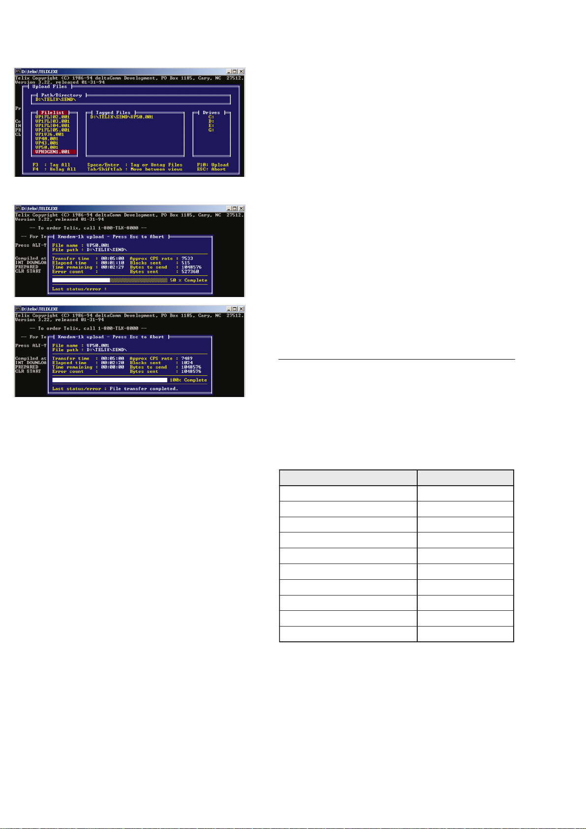
11. Now select the supplied firmware-file and press <Enter>.
12. Press <F10> and wait until the download has finished.
If the message “Telix Warning, upload was aborted”
appears during download, check connections and restart at
point 6.
13. To program another board, restart at point 6 or press
<Alt> + <x> to close Telix.
SERVICE TEST PROGRAM
The Digital A/V Receiver DFR9000 is equipped with
comprehensive service & diagnostic features. The set
internal service mode provides following test loops:
• EEPROM test
• EEPROM format
• Display test
• Key/RC/Rotary test
• I2C & SPI communication test
• DAB bit error rate test
• Audio switch test
• Video switch test
• Video test patterns
• Temperature & fan test
1. Entering the service mode
To enter the service mode hold the button <PREVIOUS>
depressed while connecting mains.
The set will enter the main menu of the service mode and
display the following message:
Left part of LCD Middle part of LCD
L xx yy mm dd.dd
L...........Country code (E=EU, U=US, O=OS)
xx..........Version of front processor firmware
yy..........Version of Video Processing Board firmware
mm.......Version of Audio-DSP firmware
dd.dd....Version of DAB tuner firmware
From the main menu various test loops can be executed by
pressing dedicated keys (see table below).
To exit a certain test loop press <OK>.
pooltseT retneotyeK
tsetMORPEE1CR
tamrofMORPEE2CR
tsetyalpsiD3CR
tsetyratoR/CR/yeK4CR
tsetnoitacinummocIPS&C2IDNUOSro6CR
tsetetarrorretibBAD7CR
tsethctiwsoiduA8CR
tsethctiwsoediV0CR
snrettaptsetoediVDNUORRUSro9CR
tsetnaf&erutarepmeTYALPSIDCR
2-3
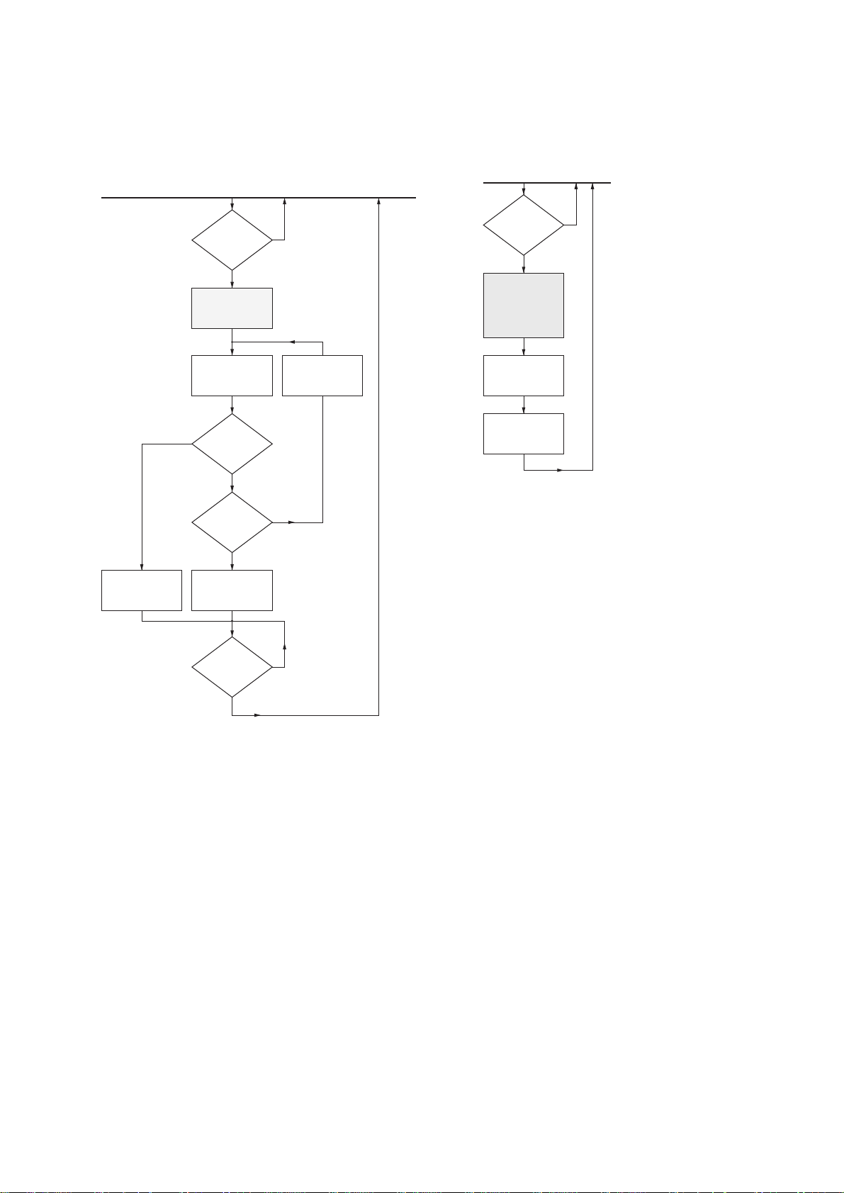
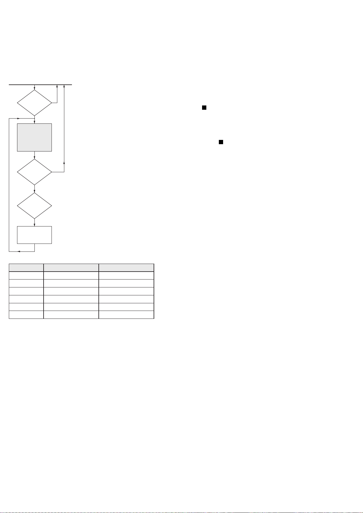
2. EEPROM test
Purpose: This test is used to check reading and writing of
data from and to the EEPROM located on the front
board.
3. EEPROM format
Purpose: Format the EEPROM located on the front board
(i.e. load the EEPROM with factory defaults).
2-4
MAIN MENU
RC “1”
pressed?
EEPROM Test
write & read back
EEPROM
test pattern
read patt. =
N
written patt.
?
N
Y
Next address
location
Y
MAIN MENU
RC “2”
pressed?
EEPROM Format
Force modules
to load the
EEPROM with
default values
Display shows
“DEFAULT”
Wait 2 seconds
N
Y
Display shows
“FAIL”
Last
address
location?
Y
Display shows
“PASS”
RC “OK”
pressed?
Y
N
N
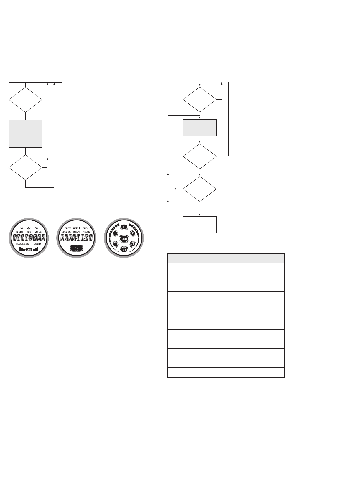
4. Display test
Purpose: This test is used to check the standby-LED, the
driving circuits and the display for short-circuits,
open circuits or other defects.
5. Key test
Purpose: This test is used to check the keys and rotaries on
the set and the reaction on commands from the
remote control.
1)
x ..........5=RC5, 6=RC6
yy.........system address
zzz.......command code
yeK yalpsiD
NO-YBDNATS1YEK
SUOIVERP2YEK
TXEN3YEK
UNEMMETSYS5YEK
DNUORRUS6YEK
ELBERT/SSAB7YEK
PUECRUOSPUCRS
NWODECRUOSNWODCRS
PUEMULOVPULOV
NWODEMULOVNWODLOV
LORTNOCETOMERzzzyyxCRYEK
)1
.tset-yekehttixeottesehtno>KO<sserP
MAIN MENU
Y
RC “4”
pressed?
RC “OK”
pressed?
N
Y
N
N
Y
Display key-code
(see table 1)
Key Test
Display shows
“--”
Key
pressed or
rotary
turned?
2-5
MAIN MENU
RC “3”
pressed?
Display Test
Display shows
Test pattern 1
Standby-LED is
blinking
RC “OK”
pressed?
N
Y
N
Y
Display Test – Test pattern 1

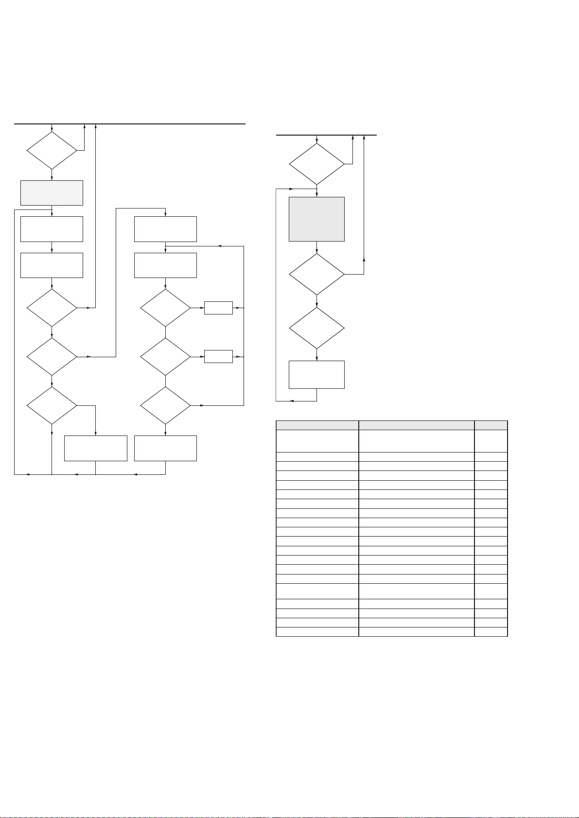
6. I2C and SPI communication test
Purpose: This test checks communication with devices
connected to the internal I2C and SPI bus.
Notes: I2C devices are tested by sending the slave address
and looking for “ACK”.
SPI devices are tested by sending certain settings
and reading them back.
Test result 1: Display shows “F xxxx xxxxxxxx”
x=“0”....test/device failed
x=“1”....test/device passed
x=“--”....test not executed
The digits (read from left to right) have following meaning:
Test result 2: Display shows “V xxxx xxxxxxxx”
x=“0”....test/device failed
x=“1”....test/device passed
x=“--”....device not tested
The digits (read from left to right) have following meaning:
tigiD eciveD
1)21WC19PMT(BPV
2detsetton-)23747CL(DSO
3)76365PSD(PSD
4)2114KA(xRFIDPS
5PIV
6MORPEERESU
7RETTIMSNARTIMDH
8REVIECERIMDH
9CNED
01AJDUORAF
111MORPEETIDE
212MORPEETIDE
tigiD eciveD
1)R2S/L2SEMULOV(B1CI
2)WBUS/CEMULOV(B1CI
3)RS/LSEMULOV(B1CI
4)R/LEMULOV(B1CI
5ELUDOMBAD
6)hctiwSoediV(8166VTS
7)CEDOC(81424SC
8BPV
9)CAD(1934SC
01desuton
11desuton
21desuton
2-6
MAIN MENU
pressed?
I2C/SPI Test
Front (step 1)
Display shows
test result 1
RC “OK”
pressed?
N
pressed?
I2C/SPI Test
VPB (step 2)
Display shows
test result 2
RC “6”
RC “6”
N
Y
Y
N
Y
N
RC “OK”
pressed?
RC “6”
pressed?
Y
N
Y
7. DAB bit error rate test
Purpose: Reads and displays the bit error rate of the DAB
tuner.
Notes: “rrr.rr” is the bit error rate in %.
“NO VALUE” is shown if no station is available. In
this case connect antenna or the test signal and
press the DAB ErrorBitRate button again. The
module will scan band III and the L band for stations
(about 2 minutes) and tune to the first station found.
It is possible to set the DAB module to a defined
center frequency. Press “RIGHT” on the RC and
229.072 MHz center frequency (228.304 till 229.840
with block name 12D) will be selected. Use “RIGHT”
and “LEFT” to select another frequency. Press the
DAB ErrorBitRate button to tune to the frequency.
7. Audio switch test
Purpose: Switches several audio modes according to the
table below. System related limitations are
ignored.
Notes: All DAC/CODEC outputs are routed to amplifiers/line
out sockets. If connecting ADC data output to all data
inputs of CODEC/DAC in parallel, input signal to
ADC will show on all outputs.
The test starts with -30dB as volume setting.
VOLUME (at least rotary) will work setting the
volume level. BASS/TREBLE will be 0dB (not
changeable). The routing will be influenced by HP
connect (HP out instead of LS). Line out and record
out is always active (L+R).
edomoiduA noitpircseD yalpsiD
lennahcitluM
rekaepsduolehtotstupnilennahcitlumkniL
erasreifilpmalla;PSDehtgnisutuohtiw
delbasiderasnoitcnufgnitumlla;delbane
NIHC_M
1golanAtuptuoehtotrenutehtkniLNIRENUT
2golanAtuptuoehtotniVTkniLNIVT
3golanAnitnorFkniLNIMAC
4golanAniDVDkniLNIDVD
5golanAniemaGkniLNIEMAG
tsetCDA )CAD-CDA(PSDehtesutubniemaGkniLNICDA
LrotarenegenottseT zH044htiwBPVehtnorotarenegenottsetesUTFEL
CrotarenegenottseT zH044htiwBPVehtnorotarenegenottsetesURETNEC
RrotarenegenottseT zH044htiwBPVehtnorotarenegenottsetesUTHGIR
RSrotarenegenottseT zH044htiwBPVehtnorotarenegenottsetesURRAER
LSrotarenegenottseT zH044htiwBPVehtnorotarenegenottsetesULRAER
WBUSrotarenegenottseT zH044htiwBPVehtnorotarenegenottsetesUWBUS
ximnwodLrotarenegenottseT zH044htiwBPVehtnorotarenegenottsetesULNWOD
ximnwodRrotarenegenottseT zH044htiwBPVehtnorotarenegenottsetesURNWOD
1xaoC
dnaSTDroDDfiedoced,nilatigidesU
rekaepsduolehtotrefsnart
NI1XAOC
2xaoCnilatigidesUNI2XAOC
3xaoCnilatigidesUNI3XAOC
lacitpOnilatigidesUNITPO
metitsrifhtiwniagatratS
MAIN MENU
Video Switch
Test
Display audio
mode
(see table 3)
RC “8”
pressed?
RC “OK”
pressed?
N
Y
RC “8”
pressed?
Y
N
Select next
audio mode
(see table 3)
2-7
MAIN MENU
RC “7”
pressed?
DAB Bit Error
Rate Test
tune to first station
in the DAB
data base
display
“ffff.fff” + “ rrr.rr” or
“ ” + “NO VALUE”
RC “OK”
pressed?
N
Y
clear DAB data base
set frequency to
229.072MHz
display frequency
“ffff.fff”
Y
N
RC
“LEFT”
pressed?
N
Y
dec. freq.
RC
“RIGHT”
pressed?
N
RC “7”
pressed?
N
Y
Y
display
“ SCAN ”
scan band III and L
RC
“RIGHT”
pressed?
N
RC “7”
pressed?
Y
display
“ SCAN ”
scan frequency
Y
inc. freq.
N

8. Video switch test
Purpose: Switches several video modes according to the
table below. System related limitations are
ignored.
Note: Video signal is shown on the video outputs without
any enhancement.
9. Video test patterns
Purpose: Activates video test patterns of the following ICs in
sequential order: Denc → Faroudja → VIP → OSD
→ HDMI receiver → HDMI transmitter
erutciP ecruoS noitpircseD yalpsiD
rabroloCcneDnoitarenegkcolcPIVdnaCNEDskcehC1CNED
rabroloCajduoraFnoitarenegkcolcPIVdnaCNED,ajduoraFskcehC1RAF
neercseulBPIVoediV-SdnaSBVCnoCNEDdnaPIVskcehC1PIV
egasseM
neercs
DSOoediV-SdnaSBVCnoCNEDdnaPIV,DSOskcehC1DSO
egasseM
neercs
ajduoraF
skcehchguortpoollluF
XRIMDH-XTIMDH-ajduoraFdnaCNED-PIV-DSO
1POOL
egasseM
neercs
ajduoraF
skcehchguortpoollluF
XRIMDH-XTIMDH-ajduoraFdnaCNED-PIV-DSO
2POOL
metitsrifhtiwniagatratS
edomoediV noitpircseD yalpsiD
)tnorf(niSBVCMAC
tnorfmorfSBVC
WOL=61niP,WOL=8niP
VCMAC
niSBVCVT
1raermorfSBVC
WOL=61niP,HGIH=8niP
VCVT
niSBVCEMAG
2raermorfSBVC
WOL=61niP,HGIH=8niP
VCEMAG
niSBVCWR-DVD
3raermorfSBVC
WOL=61niP,HGIH=8niP
VCWRDVD
)tnorf(nioediV-SMAC
tnorfmorfSBVC
otFRCSetirW)FRCS(tesffodaeR
WOL=61niP,oediV-Sdna8nip
VSMAC
nioediV-SVT
1raermorfoediV-S
otFRCSetirW)FRCS(tesffodaeR
WOL=61niP,oediV-Sdna8nip
VSVT
nioediV-SEMAG
2raermorfoediV-S
otFRCSetirW)FRCS(tesffodaeR
WOL=61niP,oediV-Sdna8nip
VSEMAG
nioediV-SWR-DVD
3raermorfoediV-S
otFRCSetirW)FRCS(tesffodaeR
WOL=61niP,oediV-Sdna8nip
VSWRDVD
4ni-VCVUY
daerniSBVC+VUY
HGIH=8niP,HGIH=61niP
1OEDIV
5ni-VCVUY
daerniSBVC+VUY
DIM=8niP,HGIH=61niP
2OEDIV
metitsrifhtiwniagatratS
2-8
MAIN MENU
RC “0”
pressed?
Video Switch
Test
Display video
mode
(see table 2)
RC “OK”
pressed?
RC “0”
pressed?
N
Y
Y
N
MAIN MENU
RC “9”
pressed?
Video Test
Patterns
Display video
test pattern
(see table 4)
RC “OK”
pressed?
RC “9”
pressed?
N
Y
Y
N
Select next
video mode
(see table 2)
Select next
video test pattern
(see table 4)
10. Temperature & fan test
Purpose: This test measures the temperature inside the set
and switches the fan speed for both fans in
parallel.
Note: “FAN FAIL” indicates fan current out of range.
Standby-LED Blinking State
When the set is in standby mode and the Standby-LED is
blinking, the internal protection circuits have detected a
serious problem and the set won’t wake up anymore.
Errors are reported via the “ERR_FLAG” line, which can be
triggered from following circuitries:
• DC protection on UCD Amplifiers
(see UCD , components around transistor 7212)
→ Most likely, one of the UCD Amplifiers is defective and
must be replaced.
• Overvoltage protection for +5V and +12V on ASP Board
(see ASP Board , components around transistor 7604)
→ Most likely, Power Supply AC6750 is defective and
must be replaced.
6
2
petstseT trapDCLtfelyalpsiD trapDCLthgiryalpsiD
ffonaf&pmeTnierutarepmeT °CFFO
tnerrucnaFnierutarepmeT °CLIAFNAFroGNINRUT
llufnaFnierutarepmeT °C3DEEPS
flah>naFnierutarepmeT °C2DEEPS
flah<naFnierutarepmeT °C1DEEPS
wolnaFnierutarepmeT °C0DEEPS
2-9
MAIN MENU
RC
“DISPLAY”
pressed?
Temperature &
Fan Test
Set fan step and
display temp.
(see table 6)
RC “OK”
pressed?
RC
“DISPLAY”
pressed?
N
Y
Y
N
Select next
fan step
(see table 6)
3-1 3-1
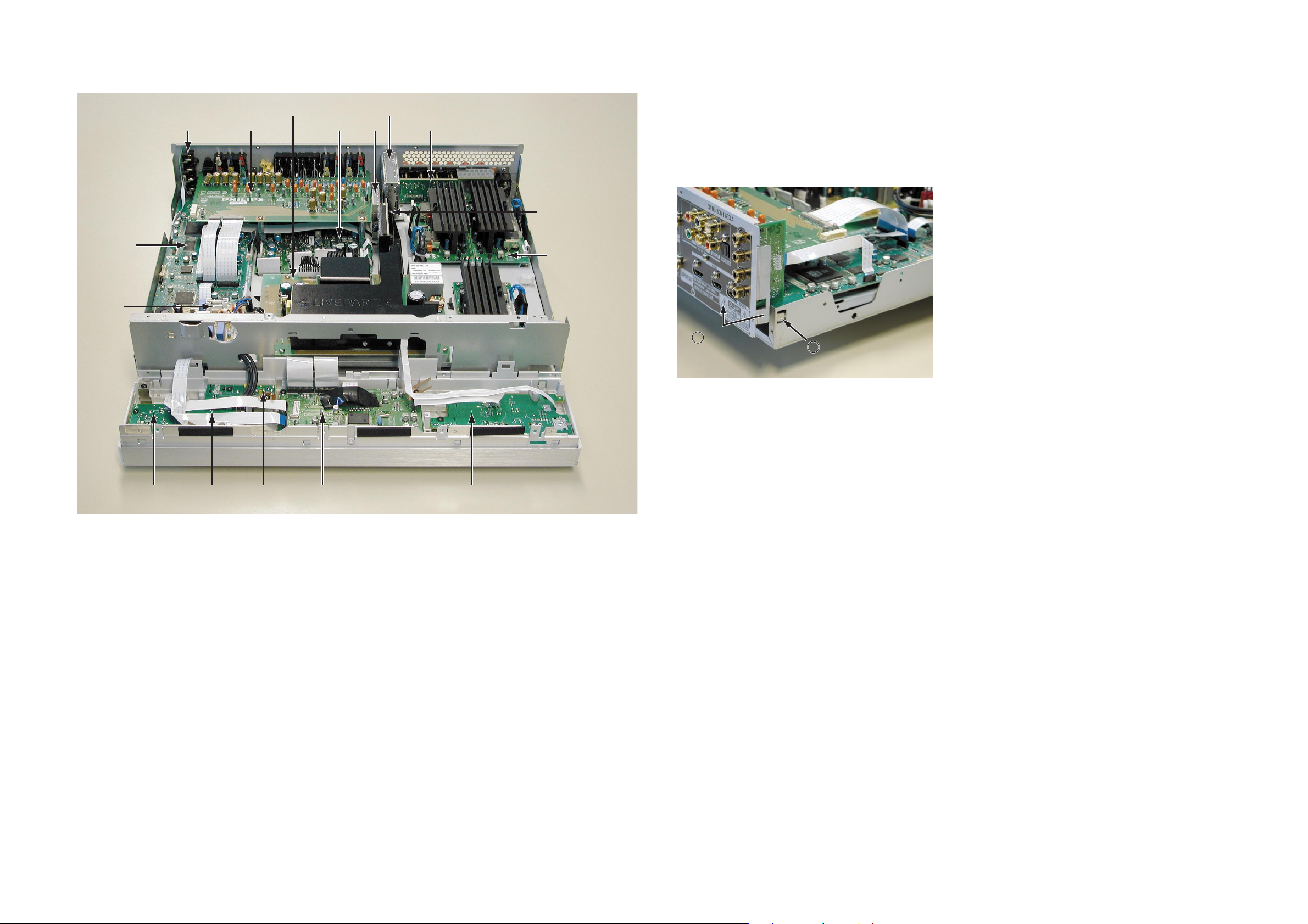
LOCATION OF PRINTED BOARDS DISMANTLING
• Remove top cover (2 screws on the left, 2 screws on the
right, 5 screws on the rear)
• Remove front (4 screws on top, 4 screws on bottom)
• Remove air channel (4 screws in corners)
• Remove safety cover
• Loosen frame screws (2 screws on the left, 2 screws on
the right, 3 screws on the rear, 1 screw on the bottom)
• Loosen snaps and pull out frame as shown below
Power Supply
Video I/O DABASP
AM/FM Tuner
Speaker TerminalDigital I/O
DAB Interface
Standby
Supply
VPB
Front Left Front I/OFront Keys Front Control Front Right
UCD Amplifier (3x)
Pull out frame
2
Loosen left&right snap
1
3-2 3-2
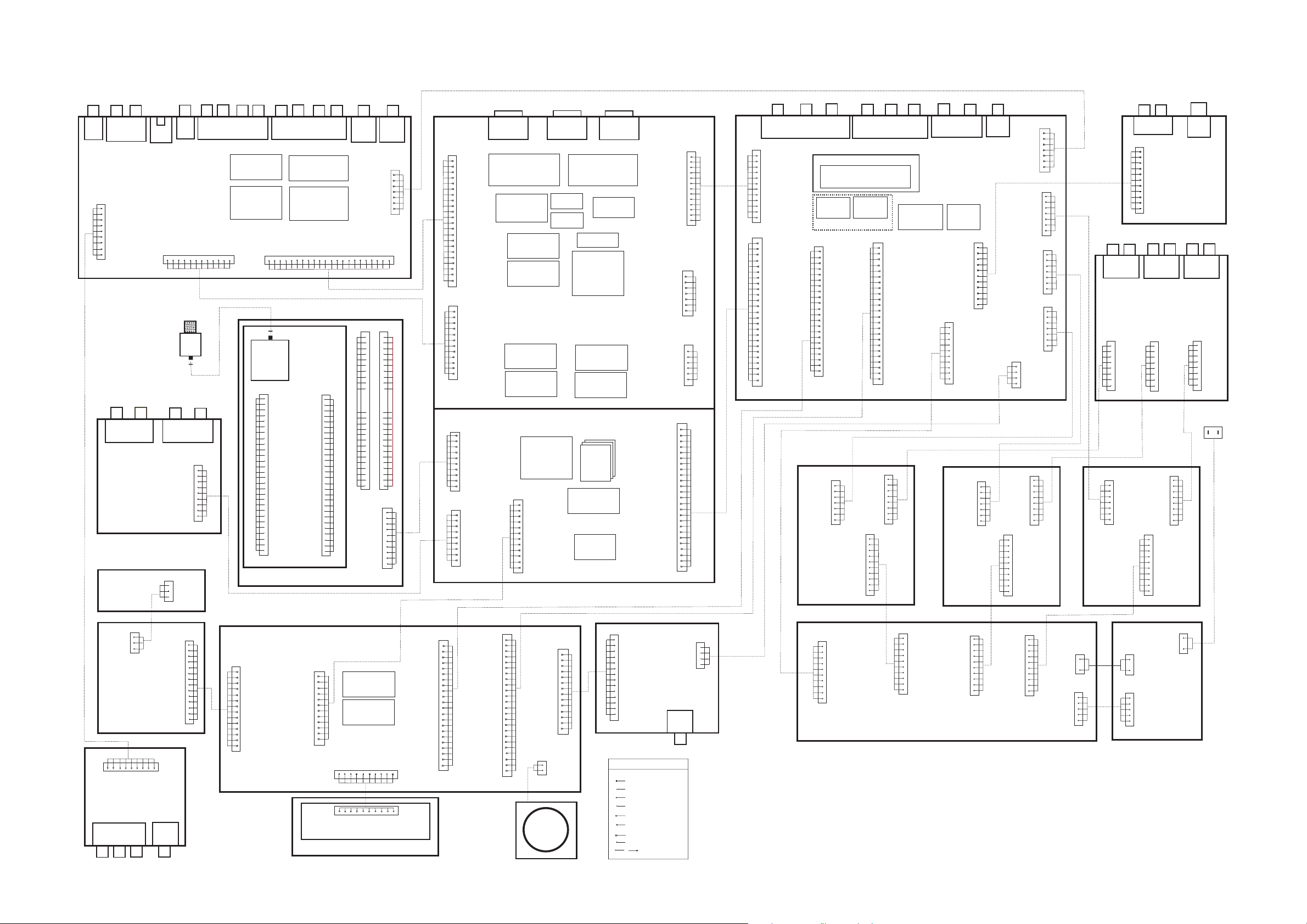
BLOCK & WIRING DIAGRAM
DIG
LINE
IN 4
OUT
OPT
7260
1261
1150
1
AINFR
GND_A
AINFL
CVBSFIN
GND_V
NC
CFIN
GND_V
YFIN
9
PH
8017
SHIELDED
DIG
OUT
COAX
DIGITAL I/O
BOARD
FRONT LEFT
KEY_2’
GND_KEY2
GND_KEY2
FRONT KEYS
1
1447
AINFL
AINFR
GND_A
FRONT I/O
1446 1445
AUDIO
L/R
IN
Y/Pb/Pr/
CVBS
OUT
SCART
CTRL
1264
CVBS
OUT
1266
VIDEO
I/O
BOARD
C_DC_LEVEL
+5V
+5V
1152
12
DIG
IN 3
COAX
1702 1703
1423
FE
NC
GND_V
CVBSFIN
CVBS
IN
8001
1
3
BL_ROT_SRC
NTC_FRONT
ROT_SRC_B
ROT_SRC_A
GND_KEY2
POWER_KEY
YFIN
CFIN
GND_V
DIG
IN 2
COAX
SPDIF_1
SPDIF_2
SPDIF_3
SPDIF_OUT
1430
3
1
FE
GND_D
LED_STBY
GND_D
KEY_2
GND_D
+5V_UP
GND_D
+12V
9
PH
S-VIDEO
IN
+3V3
GND
GND
GND
GND
KEY_2’
GND_KEY2
GND_KEY2
GND
DAB
1422
FMN
GND
VIO_SCL
COAX
1701
FMN
S-VID
VIO_SDA
DIG
IN 1
1
14
S-VID
CVBS
REC
OUT
DVD
IN
VIDEO SW
STV6618
REC
OUT
FRONT IN
NJM2285
GND
+12V
-5V
SPDIF_4
GND
FMN
1
SHIELDED
28
25
9
1
DAB INTERFACE BOARD
FRONT CONTROL BOARD
1113
1
GND_D
14
BL_ROT_SRC
LED_STBY
GND_D
NTC_FRONT
ROT_SRC_B
ROT_SRC_A
KEY_2
GND_KEY2
POWER_KEY
GND_D
+5V_UP
GND_D
+12V
FMN
8000
CVBS
DVD
IN
SW
1153
22
DAB
FRONTEND
JP 1
19
6
1
BTB
S-VID
TV
IN
R_V_IN
GND
B_U_IN
5V_RF
GND
5V
GND
DNC
DNC
DNC
DNC
DNC
GND
DNC
DNC
DNC
DNC
DNC
DNC
DNC
DNC
DNC
DNC
DNC
DNC
NRST
DNC
DNC
GND
3V3_OUT
GND
VP_I2C_SCL
VP_I2C_SDA
C_DC_LEVEL
DAB_RESET
CVBS
GND
VP_RESET
CEC_CTRL
DAB_SCL
DAB_SDA
DSP_MUTE
CVBS
S-VID
GAME
IN
12511255
CVBS SW
NJM2286
SW
HEF4051
GND
C_IN
GND
CVBS_Y_IN
GND
GND
8013
GAME
IN
R_V_OUT
GND
B_U_OUT
TV
IN
C_DC_LEVEL
G_Y_IN
DAB
TUNER
JP 2
28
AGND
AOUTL
AGND
AOUTR
AGND
AGND
SPDIF
22
DNC
DNC
DNC
DNC
(INT0)DNC
DNC
17
DNC
DNC
DNC
DNC
DNC
DNC
DNC
DNC
GND
GND
M_SCL
SDA
6
SCL
M_SDA
IR
1
BTB
1114
GND_D
GND_D
FMN
1109
0002
1
12
10
VP_IRQ
DISPLAY BOARD
FRONT
SUR
Y/Pb/Pr/
CVBS
IN 2
1265
CAM_L
GND_A
CAM_R
GND_A
LINE_OUT_L
GND_A
LINE_OUT_R
GND
G_Y_OUT
GND
Y_OUT
GND
C_OUT
GND
8014
1001 1002
BTB
+5V
+5V
GND
GND
DAB_SCL
DAB_SDA
DAB_RESET
GND
DAB_SPDIF
GND
CPU
TMP88CU77
RDS
SAA6581
GND
LCD_I2C_SDA
LCD_I2C_SCL
GND
LCD_VCCNC+LED_1_2
LCD
Y/Pb/Pr/
CVBS
IN 1
1260
1151
FMN
CVBS_OUT
FMN
1
BTB
1003
10
FMN
+LED_3_4
+LED_5_6
GND_LED
1
1
7
1
8016
+5V3_STBY
PWR_ON
PWR_DOWN
ERR_FLAG
NTC_AMP
FREQU_AMP
FREQU_AMP
TU_RDS_MPX
TU_DATA
TU_STEREO
LEVEL_LIM
FE
WTB
8011
GND_D
+5V6
+5V6
GND_D
+12V
GND_D
GND_T
GND_D
TU_CE
TU_CLK
TU_SD
HDMI
OUT
AMP_ON_LR
GND_D
MUTE_LR
MUTE_SUR
MUTE_CF
MUTE_CR
MUTE_SUB
MUTE_HP
GND
MDAC_SR
GND_D
AF_I2C_SDA
CODEC_RST
CODEC_INT
GND_D
1003
HDMI TX
SiI9030
CPU 16Bit
TMP91CW12
DENC
ADV7320
VIP
SAA7119
HDMI
VIDEO PROCESSING
BOARD
OSD
LC74732W
DC/DC
3V3
1011
1
HW_RESET
IRQ_SET
CEC
HW_SCL
HW_SDA
GND
C_DC_LEVEL
GND
DAB_SCL
DAB_SDA
DAB_RESET
DSP_MUTE
12
FMN
1112
1
BL_ROT_VOL
ROT_VOL_A
ROT_VOL_B
24
FMN
1006
1
R_V_IN
GND
B_U_IN
GND
G_Y_IN
GND
C_IN
GND
CVBS_Y_IN
GND
GND
R_V_OUT
GND
B_U_OUT
GND
G_Y_OUT
GND
Y_OUT
GND
C_OUT
GND
CVBS_OUT
22
FMN
1008
1
C_DC_LEVEL
+5V
+5V
GND
GND
VIO_SCL
VIO_SDA
GND
+12V_PSC
-5V
SPDIF_IN4
GND
12
FMN
AUDIO SIGNAL PROCESSING BOARD
1002
1
+5V
+5V
GND
GND
DAB_SCL
DAB_SDA
DAB_RESET
GND
SPDIF_DAB
GND
10
FMN
1000
1
+3V3
SPDIF_IN_1
GND
SPDIF_IN_2
GND
SPDIF_IN_3
GND
SPDIF_OUT_IO
GND
9
FMN
8005
1115
1
AMP_ON_SUR
AMP_ON_CEN
MUTE_LINE_OUT
REC_OUT_OFF
SWI_CEN_SUB
AF_I2C_SCL1
AF_I2C_SCL2
AF_I2C_SCL3
AF_I2C_SCL4
22
FMN
AUDIO
DSP
56367
HP_DET
GND_D
RE_RC6
GND_KEY1
KEY1
GND_D
+5V_UP
GND_D
+5V_C
GND_D
+12V
1111
1
2
HDMI
1004
RAM
FLASH
1110
FMN
FAN_SET
GND_FAN
IN 1
FAROUDJA
SPDIF MUX
3xRAM
SPDIF RX
AK4112
SUPPLY
1
14
FAN
SET
HDMI RX
SiI9031
E2PROM
SDRAM
FLI2310
DC/DC
-5V
& Buffer
128k
x8
1.8V
1
8002
14
HDMI
IN 2
1005
8003
8004
1414
HP_DET
BL_ROT_VOL
GND_D
RE_RC6
ROT_VOL_A
ROT_VOL_B
GND_KEY1
KEY1
GND_D
+5V_UP
GND_D
+5V_C
GND_D
+12V
FMN
LEGEND
FFC TOP ENTRY 1.25
FFC SIDE ENTRY 1.25
EH TOP ENTRY
EH SIDE ENTRY
PH TOP ENTRY
PH SIDE ENTRY
FFC TOP ENTRY 1.0
FFC SIDE ENTRY 1.0
+5V_PSC
+5V_PSC
+12V_PSC
+12V_PSC
+3V3_PSC
I2C_SDA
I2C_SCL
SERVICE
MAINTENANCE
RESET
+5V/3V3
SDA_3V3
SCL_3V3
GND
DSP_BCLK
GND
DSP_WCLK
GND
DSP_MCLK
GND
DSP_LR_DWM
GND
DSP_LR
GND
DSP_SLR
GND
DSP_CEN_SUB
GND
DSP_BACK_SUR
GND
ADC_LR
GND
ADC_MCLK
GND
ADC_BCLK
GND
ADC_WCLK
GND
FRONT RIGHT
SPECIAL
GND
GND
GND
GND
GND
SERVICE
1012
TXD
RXD
NC
GND
WE
+5V
PH
1013
NC
GND
FMN
1015
FMN
HP_LEFT
GND_A
HP_RIGHT
GND_A
1416
HP
SOCKET
1009
PH
L/R
1101
1601
1
22
GND_L
GND_R
DC_DET
CENTRE
ASP 8 CHANNEL
CS42418
FMN
IN_L
IN_R
ENA
HOP
L/R
7.1 MULTI CHANNEL INPUT
1600
8020
1
12
PH
1400
1
25
FMN
+5V
+5V
GND_D
GND_D
+12V
+12V
GND_D
GND_D
+3V3
CODEC_I2C_SDA
CODEC_I2C_SCL
GND_D
GND
DSP_BCLK
GND
DSP_WCLK
GND
DSP_MCLK
GND
DSP_LR_DWM
GND
DSP_LR
GND
DSP_SLR
GND
DSP_CEN_SUB
GND
DSP_BACK_SUR
GND
ADC_LR
GND
ADC_MCLK
GND
ADC_BCLK
GND
ADC_WCLK
GND
1
12
1
7
1
6
1
8012
UCD
25
1417
1
4
FE
AMP
MAIN
0007
1
10
EH
POWER SUPPLY BOARD AC6750
BACK SUR
LFE
L/R, SL/SR, LFE/C, SC
ADC
2CH
+5V3_STBY
GND_D
+5V6
+5V6
GND_D
+12V
GND_D
PWR_ON
PWR_DOWN
ERR_FLAG
NTC_AMP
FREQU_AMP
FREQU_AMP
GND_T
TU_RDS_MPX
GND_D
TU_CE
TU_DATA
TU_CLK
TU_SD
TU_STEREO
LEVEL_LIM
1201
+5V3_EVER
GND_A
+12V
PWR_ON
FREQ_PWR
GND_D
GND_D
+5V6
NTC
CURR_DET
4x TDA7468
8019
1
7
FE
+VB_AMP
+VB_AMP
+VB_AMP
GND_AMP
GND_AMP
GND_AMP
-VB_AMP
-VB_AMP
-VB_AMP
NTC
L/R
DAC
8CH
24
GND_ML
GND_ML
SP_ML
SP_ML
SP_MR
SP_MR
GND_MR
GND_MR
1100
1603
1
FMN
EH
IN
1
10
GAME
TV
IN
1108
AMP_ON_LR
AMP_ON_SUR
AMP_ON_CEN
GND_D
MUTE_LR
MUTE_SUR
MUTE_CF
MUTE_CR
MUTE_SUB
MUTE_HP
MUTE_LINE_OUT
GND
REC_OUT_OFF
SWI_CEN_SUB
MDAC_SR
GND_D
AF_I2C_SDA
AF_I2C_SCL1
AF_I2C_SCL2
AF_I2C_SCL3
AF_I2C_SCL4
CODEC_RST
CODEC_INT
GND_D
8006
1110
1
8
EH
8021
1
10
EH
IN
AUDIO
I/O
BOARD
DAC 2CH
CS4391
+AMP
+AMP
+AMP
GND_AMP
GND_AMP
GND_AMP
-AMP
-AMP
-AMP
NTC
DVD
1100
DC/DC
TU_SD
TU_RDS_MPX
TU_CE
TU_DATA
TU_STEREO
TU_CLK
1602
1
10
EH
GND_SR
UCD
AMP
SURR
+AMP
+AMP
+AMP
GND_AMP
GND_AMP
GND_AMP
REC
OUT
-12V
GND
NC
+9V0
TU_R
TU_L
+5V3_EVER
GND_A
+12V
PWR_ON
FREQ_PWR
GND_D
GND_D
+5V6
NTC_AMP
CURR_DET
8007
8024
IN_SL
GND_SL
IN_SR
ENA
DC_DET
HOP
0005
-AMP
-AMP
-AMP
NTC
EH
1118
FE
1201
FE
11
1
10
1
SUBW
OUT
1103
1
7
8022
LINE_OUT_L
LINE_OUT_R
AMP_ON_CEN
AMP_ERR
FREQ_AMP
AMP_ON_SUR
FREQ_AMP
AMP_ON_LR
FREQ_AMP
1117
1
4
FE
GND_SL
GND_SL
SP_SL
SP_SL
SP_SR
SP_SR
GND_SR
GND_SR
1100
1
10
EH
+AMP
+AMP
+AMP
GND_AMP
GND_AMP
GND_AMP
-AMP
-AMP
-AMP
NTC
CAM_L
GND_A
CAM_R
GND_A
GND_A
AMP_CF
GND_A
AMP_CR
GND_A
AMP_SL
GND_A
AMP_SR
GND_A
AMP_ERR
AMP_L
GND_A
AMP_R
GND_A
AMP_ERR
HP_L
GND_A
HP_R
GND_A
1110
+VB_AMP
+VB_AMP
+VB_AMP
GND_AMP
GND_AMP
GND_AMP
-VB_AMP
-VB_AMP
-VB_AMP
NTC
0001
EH
EH
1
10
1106
1
7
FMN
1116
FE
1113
FE
1110
FE
8008
1
8
NEUTRAL
HOT_SWD
PWR_ON
+5V3_EVER
AMAE
FL FR
1801
0001
1
GND
NC
TU_SD
+9V0
TU_RDS_MPX
TU_R
TU_CE
TU_L
TU_DATA
TU_STEREO
TU_CLK
11
FE
SL SR CF CR
1802 1803
SPEAKER
TERMINAL
8015
8010
1
8009
7
1
7
1
FM
AM&FM
TUNER
BOARD
7
+12V
GND
GND
0002
0004
EH
VH
1804
1
8
EH
1201
1
7
FE
UCD
AMP
CENTER
8023
1
8029
3
1
8030
5
GND_ML
GND_ML
SP_ML
SP_ML
SP_MR
SP_MR
GND_MR
GND_MR
8025
IN_CF
GND_CF
IN_CR
GND_CR
ENA
DC_DET
HOP
1
3
1
5
1001
VH
1002
EH
1805
1
8
EH
GND_CF
GND_CF
SP_CF
SP_CF
SP_CR
SP_CR
GND_CR
GND_CR
1100
1
10
EH
MAINS_NE
MAINS_HOT
NEUTRAL
HOT_SWD
+12V
GND
PWR_ON
GND
+5V3_EVER
+VB_AMP
+VB_AMP
+VB_AMP
GND_AMP
GND_AMP
GND_AMP
-VB_AMP
-VB_AMP
-VB_AMP
NTC
STANDBY
SUPPLY
BOARD
GND_SL
GND_SL
SP_SL
SP_SL
SP_SR
SP_SR
GND_SR
GND_SR
1110
EH
1806
1
GND_CF
GND_CF
SP_CF
SP_CF
SP_CR
SP_CR
GND_CR
GND_CR
8
EH
MAINS
8026
1
8
10000006
1
8028
3
VH

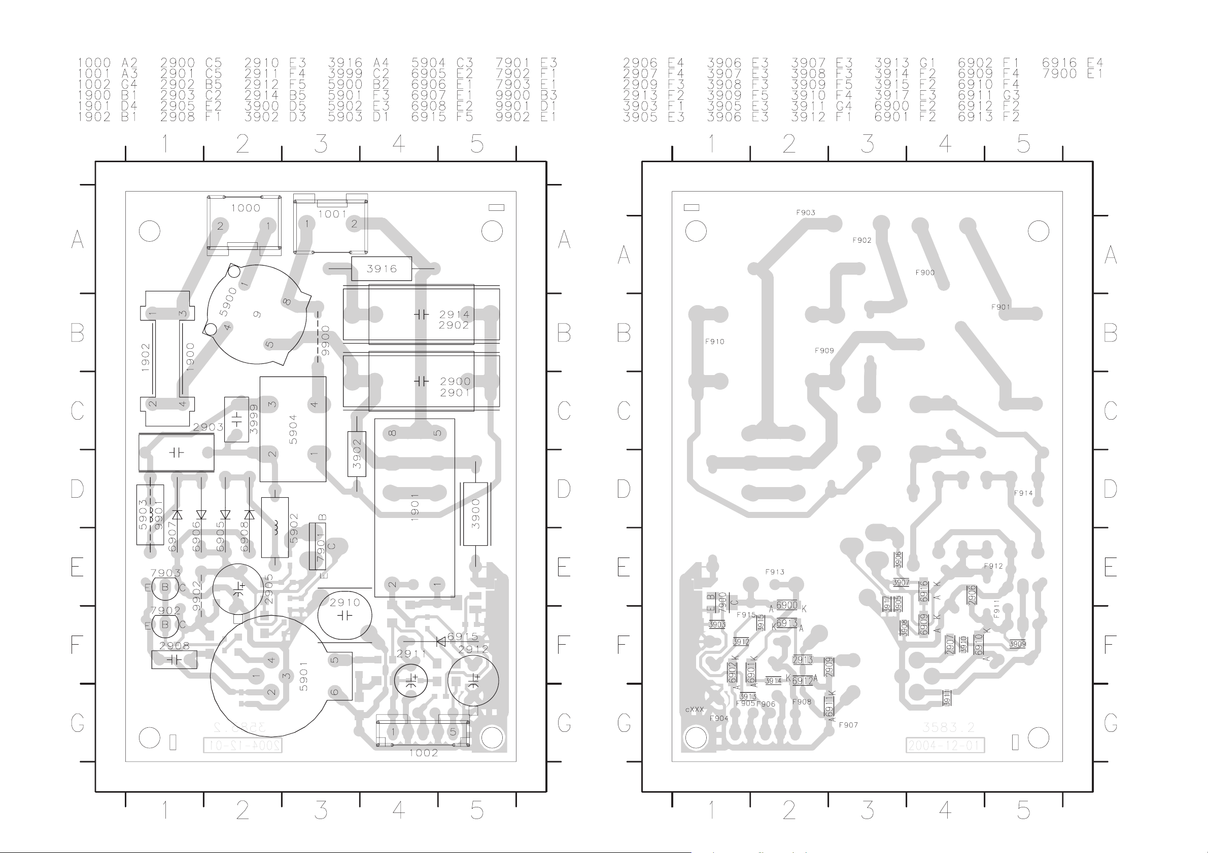
4-1 4-1
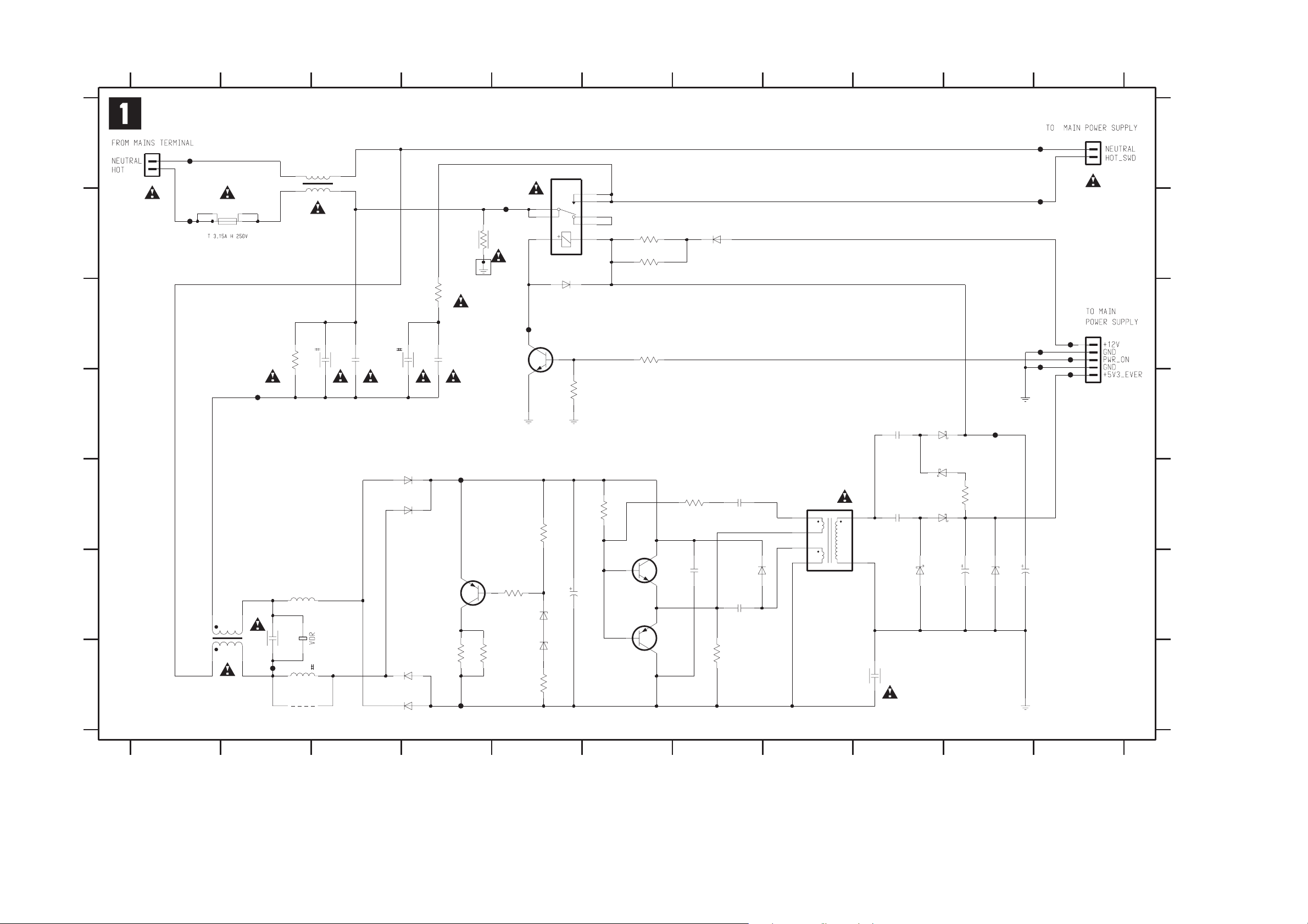
Standby Power Supply
This board is not intended to be repaired on component level.
Circuit Diagrams and Printed Circuit Board drawings
are published for orientation only.
In case of defects please replace the entire board.
Boards can be ordered with codenumber “3103 308 68331”.
4-2 4-2
A
B
C
D
E
F
G
B2P3-VH
# ...... not used
123
STANDBY POWER SUPPLY
1000
F900
1
2
F901
1902
1900
PTF/65
5904
UF1717V
F910
21
2903
34
F914
5900
18
45
2004TS-035
2M2
2900
470n
100n
3902
5902
1m0
3999
5903
1m0
9901
2901
220n
2914
6905
1N4003
6906
1N4003
6907
1N4003
6908
1N4003
4567891011
F904
F908
1001
1
2
B2P3-VH
B5B-EH-A
5
4
3
2
1
1002
470n
3916
2902
220R
220n
3905
F911
7901
BD438
F912
3900
220R
3917
220R
F909
10M
1901
NO
COM
4
73
NC
12
OZ
BAS316
6900
F915
7900
BC817-40
3903
3907
330R
3906
6916
6909
3908
2905
PDZ18-B
PDZ22-B
330R
680R
10K
100u
F902
5
8
6
3912
220R
3915
220R
3913
100R
4M7
3909
7902
BC547B
7903
BC557B
3910
330R
2906
6902
BAS316
100n
3911
100K
2907
100n
2908
4n7
6910
BAS316
6911
6913
BAT54 COL
BAT54 COL
6901
6912
BAT54 COL
2911
BAT54 COL
2913
100n
5901
4
2
1
3
3A1631N
2909
5
100n
6
470p
2910
3914
330R
22u
F913
6915
F905
F907
2912
BZX79-C5V6
F903
F906
220u
A
B
C
D
E
F
G
1000 A1
1001 A11
1002 D11
1900 B2
1901 A5
1902 B2
2900 C3
2901 C3
2902 C4
2903 F2
2905 F5
2906 F7
2907 E7
2908 F7
2909 E9
2910 G9
2911 F10
2912 F10
2913 D9
2914 C4
3900 B4
3902 C2
3903 D5
3905 G4
3906 F5
3907 E5
3908 G5
3909 E6
3910 E7
3911 G7
3912 B6
3913 C6
3914 E10
3915 B6
3916 C4
3917 G4
3999 F2
5900 A3
5901 E8
5902 F2
5903 G2
5904 F2
6900 C5
6901 E9
6902 B7
6905 E4
6906 E4
6907 G4
6908 G4
6909 G5
6910 F7
6911 F9
6912 E9
6913 D9
6915 F10
6916 F5
7900 C5
7901 F4
7902 F6
7903 F6
9901 G2
F900 A1
F901 B1
F902 A11
F903 B11
F904 C11
F905 C11
F906 C11
F907 D11
F908 D11
F909 B5
F910 D2
F911 E4
F912 G4
F913 D10
F914 G2
F915 C5
1234567891011
4-3 4-3
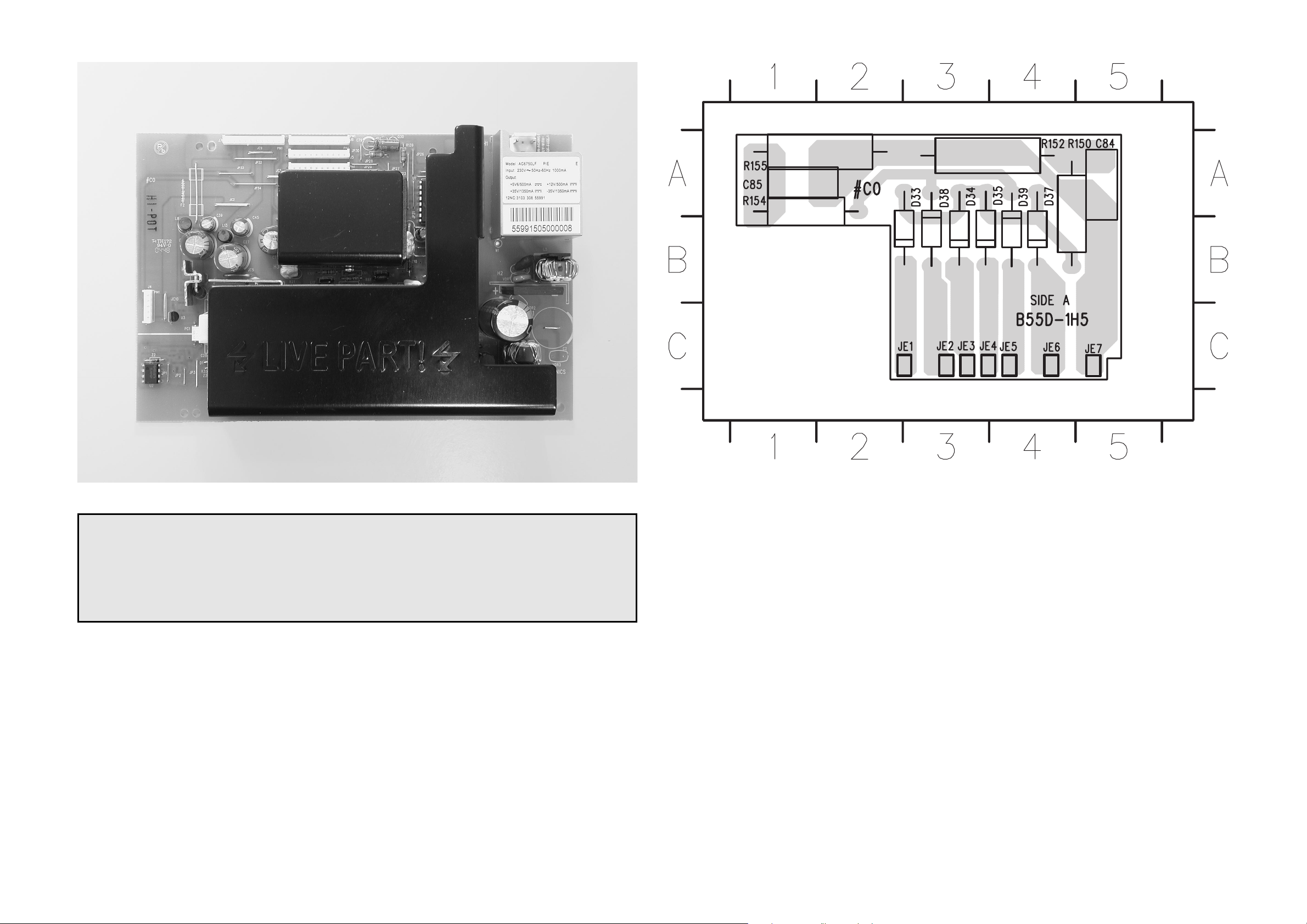
5-1 5-1
Power Supply AC6750
This board is not intended to be repaired on component level.
Circuit Diagrams and Printed Circuit Board drawings
are published for orientation only.
In case of defects please replace the entire board.
Boards can be ordered with codenumber “3103 308 55991”.

5-2 5-2
1 234567891011
12 13
POWER SUPPLY AC6750
A
*
B
*
*
*
C
A
B
C
G
D
*
E
F
D
E
F
G
H
* not used
1 2 56789101112 13
34
H
5-3 5-3
5-4 5-4

6-1 6-1
Front Control
This board is not intended to be repaired on component level.
Circuit Diagrams and Printed Circuit Board drawings
are published for orientation only.
In case of defects please replace the entire board.
Boards can be ordered with codenumber “9965 000 26719”.
 Loading...