

Philips BFQ135 Datasheet

DISCRETE SEMICONDUCTORS
DATA SH EET
BFQ135
NPN 6.5 GHz wideband transistor
Product specification
Supersedes data of September 1995
File under Discrete Semiconductors, SC14
1997 Nov 07

Philips Semiconductors Product specification
NPN 6.5 GHz wideband transistor BFQ135
FEATURES
• Optimum temperature profile and
excellent reliability properties
ensured by emitter-ballasting
resistors and application of gold
sandwich metallization.
DESCRIPTION
NPN wideband transistor in a 4-lead
dual-emitter SOT172A2 package with
a ceramic cap. All leads are isolated
from the mounting base.
page
4
3
1
PINNING
APPLICATIONS
2
PIN DESCRIPTION
• MATV and microwave amplifiers,
such as in aerial amplifiers, radar
systems, oscilloscopes, spectrum
analysers, etc.
1 collector
2, 4 emitter
3 base
Top view
Fig.1 SOT172A2.
MSA457
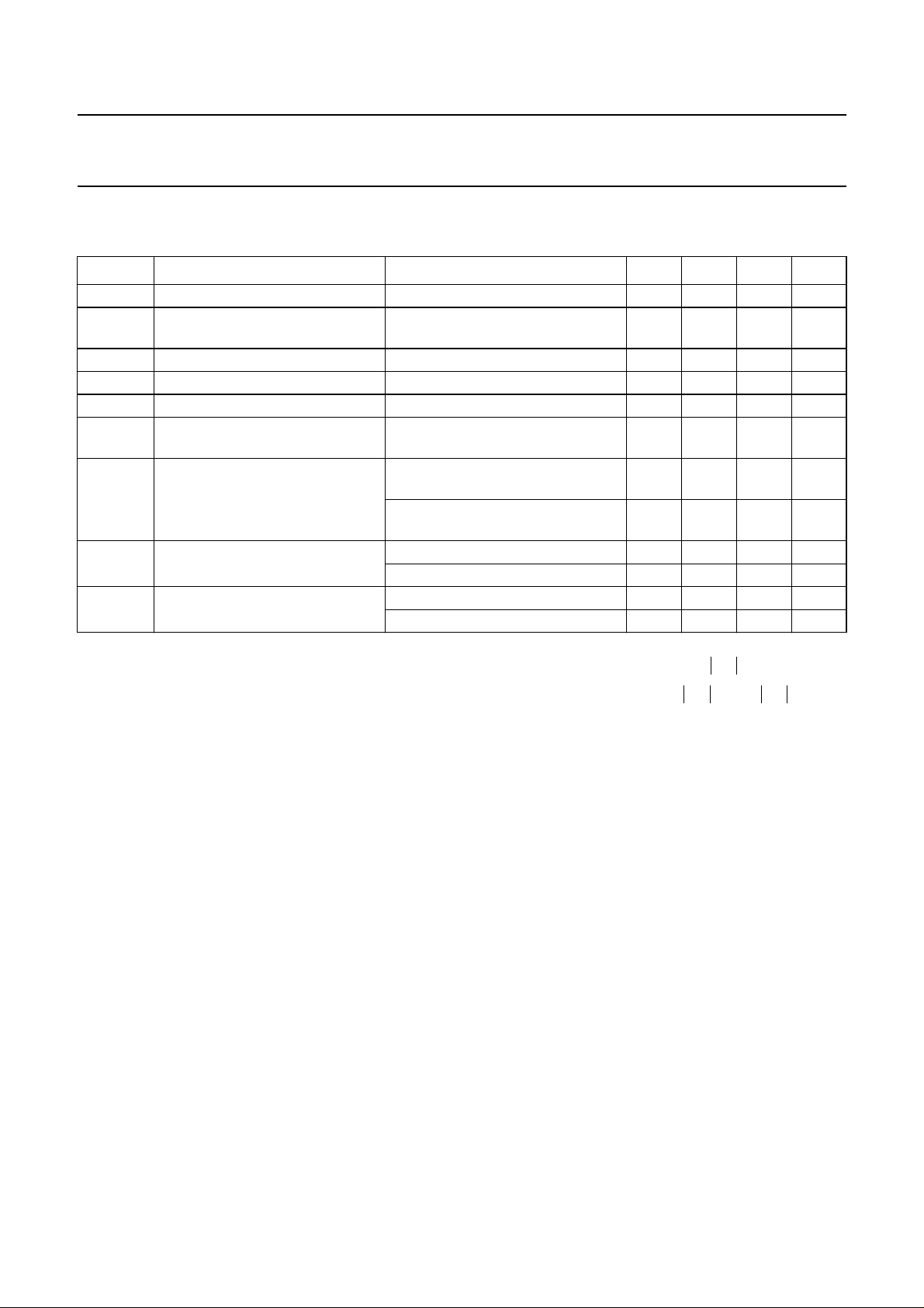
QUICK REFERENCE DATA
SYMBOL PARAMETER CONDITIONS MIN. TYP. MAX. UNIT
V
CEO
I
C
P
tot
h
FE
f
T
G
UM
V
O
collector-emitter voltage open base −−19 V
collector current (DC) −−150 mA
total power dissipation Tc≤ 145 °C −−2.7 W
DC current gain IC= 120 mA; VCE= 18 V; T
transition frequency IC= 120 mA; VCE= 18 V; f = 1 GHz;
T
=25°C
amb
maximum unilateral power gain IC= 120 mA; VCE= 18 V; f = 500 MHz;
=25°C
T
amb
I
= 120 mA; VCE= 18 V; f = 800 MHz;
C
T
=25°C
amb
output voltage dim= −60 dB; IC= 120 mA; VCE=18V;
=25°C55 −−
amb
− 6.5 − GHz
− 17 − dB
− 13.5 − dB
− 1.2 − V
RL=75Ω; fp+fq−fr= 793.25 MHz;
T
=25°C
amb
WARNING
Product and environmental safety - toxic materials
This product contains beryllium oxide. The product is entirely safe provided that the BeO disc is not damaged.
All persons who handle, use or dispose of this product should be aware of its nature and of the necessary safety
precautions. After use, dispose of as chemical or special waste according to the regulations applying at the location of
the user. It must never be thrown out with the general or domestic waste.
1997 Nov 07 2

Philips Semiconductors Product specification
NPN 6.5 GHz wideband transistor BFQ135
LIMITING VALUES
In accordance with the Absolute Maximum Rating System (IEC 134).
SYMBOL PARAMETER CONDITIONS MIN. MAX. UNIT
V
CBO
V
CEO
V
EBO
I
C
P
tot
T
stg
T
j
THERMAL CHARACTERISTICS
SYMBOL PARAMETER VALUE UNIT
R
th j-c
collector-base voltage open emitter − 25 V
collector-emitter voltage open base − 19 V
emitter-base voltage open collector − 2V
collector current (DC) − 150 mA
total power dissipation Tc≤ 145 °C − 2.7 W
storage temperature −65 +150 °C
junction temperature − 200 °C
thermal resistance from junction to case 20 K/W
1997 Nov 07 3
Philips Semiconductors Product specification
NPN 6.5 GHz wideband transistor BFQ135
CHARACTERISTICS
T
=25°C unless otherwise specified.
j
SYMBOL PARAMETER CONDITIONS MIN. TYP. MAX. UNIT
I
CBO
h
FE
C
c
C
e
C
re
f
T
G
UM
V
O
d
2
collector cut-off current IE= 0; VCB=18V −−50 µA
DC current gain IC= 120 mA; VCE=18V;
T
=25°C
amb
55 −−
collector capacitance IE=ie= 0; VCB= 18 V; f = 1 MHz − 1.8 − pF
emitter capacitance IC=ic= 0; VEB= 0.5 V; f = 1 MHz − 5.5 − pF
feedback capacitance IC= 0; VCE=18V; f=1MHz − 1 1.2 pF
transition frequency IC= 120 mA; VCE=18V;
maximum unilateral power gain
(note 1)
f = 1 GHz; T
IC= 120 mA; VCE=18V;
f = 500 MHz; T
I
= 120 mA; VCE=18V;
C
f = 800 MHz; T
amb
=25°C
=25°C
amb
=25°C
amb
− 6.5 − GHz
− 17 − dB
− 13.5 − dB
output voltage note 2 − 1.35 − V
note 3 − 1.2 − V
second order intermodulation
distortion
note 4 −−70 − dB
note 5 −−70 − dB
Notes
1. G
is the maximum unilateral power gain, assuming S12 is zero and .
UM
2. dim= −60 dB (DIN 45004B); IC= 120 mA; VCE= 18 V; RL=75Ω; T
Vp=VO at dim= −60 dB; fp= 445.25 MHz;
Vq=VO−6 dB; fq= 453.25 MHz;
Vr=VO−6 dB; fr= 455.25 MHz;
measured at fp+fq−fr= 443.25 MHz.
3. dim= −60 dB (DIN 45004B); IC= 120 mA; VCE= 18 V; RL=75Ω; T
Vp=VO at dim= −60 dB; fp= 795.25 MHz;
Vq=VO−6 dB; fq= 803.25 MHz;
Vr=VO−6 dB; fr= 805.25 MHz;
measured at fp+fq−fr= 793.25 MHz.
4. IC= 90 mA; VCE= 18 V; VO= 50 dBmV; T
amb
=25°C;
fp= 50 MHz; fq= 400 MHz;
measured at fp+fq= 450 MHz.
5. IC= 90 mA; VCE= 18 V; VO= 50 dBmV; T
amb
=25°C;
fp= 250 MHz; fq= 560 MHz;
measured at fp+fq= 810 MHz.
amb
amb
G
UM
=25°C;
=25°C;
=
10 log
--------------------------------------------------------------
1
S
–
11
2
S
21
2
S
–
1
˙
dB
2
22
1997 Nov 07 4
 Loading...