

Philips BF550 Datasheet

DISCRETE SEMICONDUCTORS
DATA SH EET
ook, halfpage
M3D088
BF550
PNP medium frequency transistor
Product specification
Supersedes data of 1997 Jul 07
1999 Apr 15
Philips Semiconductors Product specification
PNP medium frequency transistor BF550
FEATURES
• Low current (max. 25 mA)
• Low voltage (max. 40 V).
APPLICATIONS
• Medium frequency applications in thick and thin film
circuits.
DESCRIPTION
PNP medium frequency transistor in a SOT23 plastic
package.
MARKING
TYPE NUMBER MARKING CODE
(1)
BF550 LA∗
Note
1. ∗ = p : Made in Hong Kong.
∗ = t : Made in Malaysia.
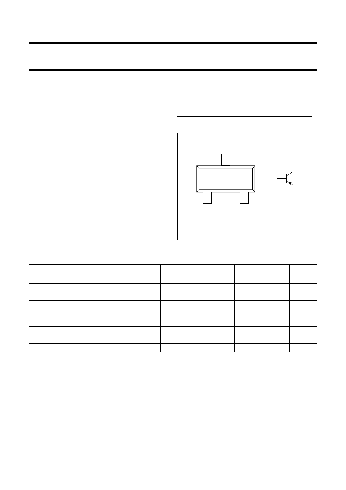
PINNING
PIN DESCRIPTION
1 base
2 emitter
3 collector
handbook, halfpage
Top view
3
1
21
MAM256
Fig.1 Simplified outline (SOT23) and symbol.
3
2
LIMITING VALUES
In accordance with the Absolute Maximum Rating System (IEC 134).
SYMBOL PARAMETER CONDITIONS MIN. MAX. UNIT
V
CBO
V
CEO
V
EBO
I
C
I
CM
P
tot
T
stg
T
j
T
amb
collector-base voltage open emitter −−40 V
collector-emitter voltage open base −−40 V
emitter-base voltage open collector −−4V
collector current (DC) −−25 mA
peak collector current −−25 mA
total power dissipation T
≤ 25 °C; note 1 − 250 mW
amb
storage temperature −65 +150 °C
junction temperature − 150 °C
operating ambient temperature −65 +150 °C
Note
1. Transistor mounted on an FR4 printed-circuit board.
1999 Apr 15 2

Philips Semiconductors Product specification
PNP medium frequency transistor BF550
THERMAL CHARACTERISTICS
SYMBOL PARAMETER CONDITIONS VALUE UNIT
R
th j-a
Note
1. Transistor mounted on an FR4 printed-circuit board.
CHARACTERISTICS
=25°C unless otherwise specified.
T
amb
SYMBOL PARAMETER CONDITIONS MIN. TYP. MAX. UNIT
I
CBO
I
EBO
h
FE
V
BE
C
re
f
T
thermal resistance from junction to ambient note 1 500 K/W
collector cut-off current IE= 0; VCB= −30 V −−−50 nA
emitter cut-off current IC= 0; VEB= −3V −−−100 nA
DC current gain IC= −1 mA; VCE= −10 V 50 −−
base-emitter voltage IC= −1 mA; VCE= −10 V − 750 − mV
feedback capacitance IC= −1 mA; VCB= −10 V; f = 1 MHz − 0.5 − pF
transition frequency IC= −1 mA; VCE= −10 V; f = 100 MHz − 325 − MHz
1999 Apr 15 3
 Loading...