

Philips bf494, bf495 Service manual
DISCRETE SEMICONDUCTORS
DATA SH EET
ook, halfpage
M3D186
BF494; BF495
NPN medium frequency transistors
Product specification
Supersedes data of September 1994
File under Discrete Semiconductors, SC04
1997 Jul 08

Philips Semiconductors Product specification
NPN medium frequency transistors BF494; BF495
FEATURES
• Low current (max. 30 mA)
• Low voltage (max. 20 V).
PINNING
PIN DESCRIPTION
1 base
2 emitter
APPLICATIONS
3 collector
• HF applications in radio and television receivers
• FM tuners
• Low noise AM mixer-oscillators
• IF amplifiers in AM/FM receivers.
DESCRIPTION
handbook, halfpage
1
2
3
1
MAM258
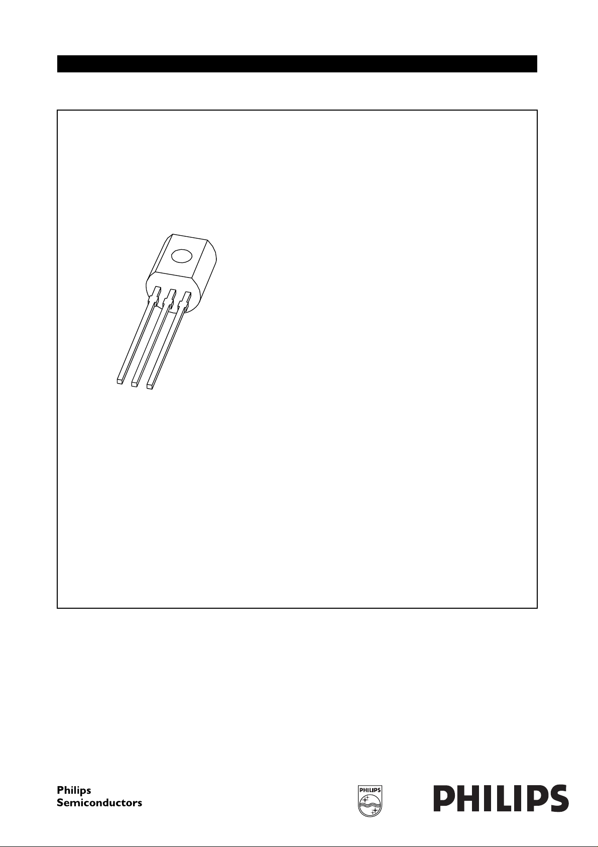
NPN medium frequency transistor in a TO-92; SOT54
plastic package.
Fig.1 Simplified outline (TO-92; SOT54)
and symbol.
QUICK REFERENCE DATA
SYMBOL PARAMETER CONDITIONS MIN. MAX. UNIT
V
V
I
P
h
CBO
CEO
CM
tot
FE
collector-base voltage open emitter − 30 V
collector-emitter voltage open base − 20 V
peak collector current − 30 mA
total power dissipation T
≤ 25 °C − 300 mW
amb
DC current gain IC= 1 mA; VCE=10V
BF494 67 220
BF495 35 125
f
T
transition frequency IC= 1 mA; VCE= 10 V; f = 100 MHz 120 − MHz
3
2
1997 Jul 08 2

Philips Semiconductors Product specification
NPN medium frequency transistors BF494; BF495
LIMITING VALUES
In accordance with the Absolute Maximum Rating System (IEC 134).
SYMBOL PARAMETER CONDITIONS MIN. MAX. UNIT
V
CBO
V
CEO
V
EBO
I
C
I
CM
P
tot
T
stg
T
j
T
amb
Note
1. Transistor mounted on an FR4 printed-circuit board.
collector-base voltage open emitter − 30 V
collector-emitter voltage open base − 20 V
emitter-base voltage open collector − 5V
collector current (DC) − 30 mA
peak collector current − 30 mA
total power dissipation T
≤ 25 °C; note 1 − 300 mW
amb
storage temperature −65 +150 °C
junction temperature − 150 °C
operating ambient temperature −65 +150 °C
THERMAL CHARACTERISTICS
SYMBOL PARAMETER CONDITIONS VALUE UNIT
R
th j-a
thermal resistance from junction to ambient note 1 420 K/W
Note
1. Transistor mounted on an FR4 printed-circuit board.
CHARACTERISTICS
=25°C unless otherwise specified.
T
amb
SYMBOL PARAMETER CONDITIONS MIN. MAX. UNIT
I
CBO
I
EBO
h
FE
collector cut-off current IE= 0; VCB=20V − 100 nA
I
= 0; VCB=20V; T
E
= 150 °C − 4 µA
amb
emitter cut-off current IC= 0; VEB=4V − 100 nA
DC current gain IC= 1 mA; VCE=10V
BF494 67 220
BF494B 100 220
BF495 35 125
BF495B 100 125
V
BE
C
re
f
T
base-emitter voltage IC= 1 mA; VCE= 10 V 650 740 mV
feedback capacitance IC= 0; VCB=10V; f=1MHz − 1pF
transition frequency IC= 1 mA; VCE= 10 V; f = 100 MHz 120 − MHz
1997 Jul 08 3
 Loading...