

Philips BF459 Datasheet
DISCRETE SEMICONDUCTORS
DATA SH EET
ook, halfpage
M3D100
BF458; BF459
NPN high-voltage transistors
Product specification
Supersedes data of 1996 Dec 06
1999 Apr 21
Philips Semiconductors Product specification
NPN high-voltage transistors BF458; BF459
FEATURES
• Low current (max. 100 mA)
• High voltage (max. 300 V).
handbook, halfpage
APPLICATIONS
2
• Intended for video output stages in black-and-white and
in colour television receivers.
3
1
DESCRIPTION
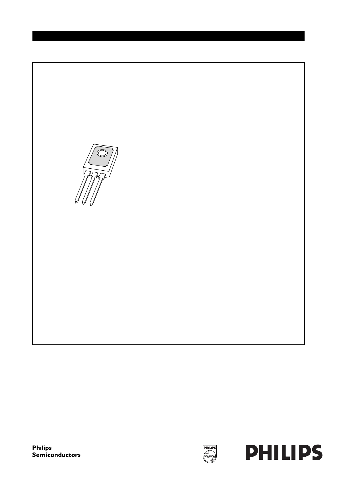
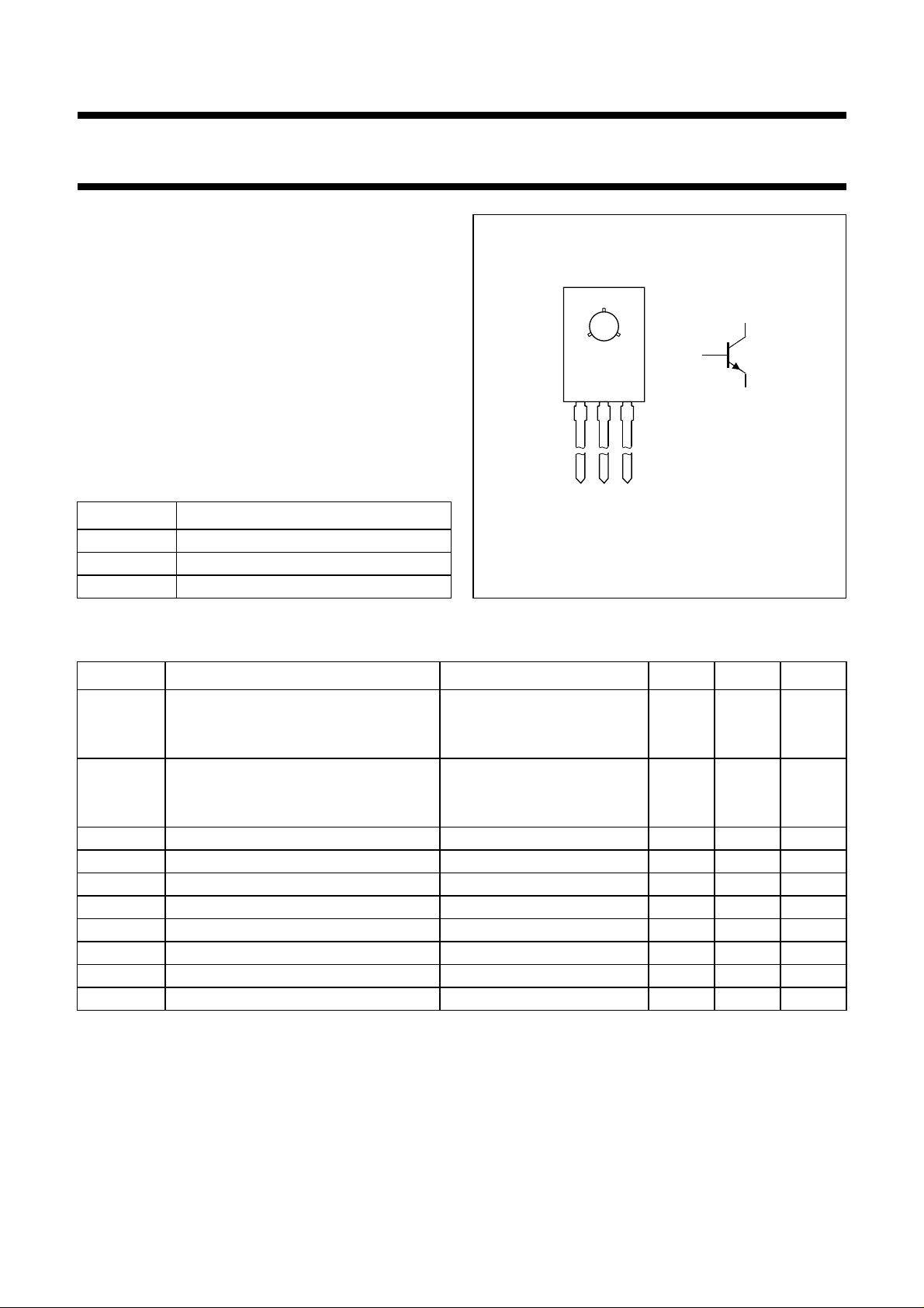
NPN transistors in a TO-126; SOT32 plastic package.
123
Top view
MAM254
PINNING
PIN DESCRIPTION
1 emitter
2 collector, connected to mounting base
Fig.1 Simplified outline (TO-126; SOT32)
and symbol.
3 base
LIMITING VALUES
In accordance with the Absolute Maximum Rating System (IEC 134).
SYMBOL PARAMETER CONDITIONS MIN. MAX. UNIT
V
CBO
collector-base voltage open emitter
BF458 − 250 V
BF459 − 300 V
V
CEO
collector-emitter voltage open base
BF458 − 250 V
BF459 − 300 V
V
EBO
I
C
I
CM
I
BM
P
tot
T
stg
T
j
T
amb
emitter-base voltage open collector − 5V
collector current (DC) − 100 mA
peak collector current − 300 mA
peak base current − 100 mA
total power dissipation Tmb≤ 90 °C − 6W
storage temperature −65 +150 °C
junction temperature − 150 °C
operating ambient temperature −65 +150 °C
1999 Apr 21 2
Philips Semiconductors Product specification
NPN high-voltage transistors BF458; BF459
THERMAL CHARACTERISTICS
SYMBOL PARAMETER VALUE UNIT
R
th j-a
R
th j-mb
CHARACTERISTICS
=25°C unless otherwise specified.
T
j
SYMBOL PARAMETER CONDITIONS MIN. TYP. MAX. UNIT
I
CBO
I
CBO
I
EBO
h
FE
V
CEsat
C
c
C
re
f
T
thermal resistance from junction to ambient 104 K/W
thermal resistance from junction to mounting base 10 K/W
collector cut-off current
BF458 I
= 0; VCB= 200 V −−50 nA
E
I
= 0; VCB= 200 V; Tj= 150 °C −−5µA
E
collector cut-off current
BF459 I
= 0; VCB= 250 V −−50 nA
E
I
= 0; VCB= 250 V; Tj= 150 °C −−5µA
E
emitter cut-off current IC= 0; VEB=5V −−100 nA
DC current gain IC= 30 mA; VCE=10V 26 −−
collector-emitter saturation
IC= 30 mA; IB=6mA −−1V
voltage
collector capacitance IE=ie= 0; VCB= 30 V; f = 1 MHz −−4.5 pF
feedback capacitance IC=ic= 0; VCE= 30 V; f = 1 MHz −−3.5 pF
transition frequency IC= 15 mA; VCE= 10 V; f = 100 MHz − 90 − MHz
1999 Apr 21 3
 Loading...