

Philips bcf81 DATASHEETS

DISCRETE SEMICONDUCTORS
DATA SH EET
BCF81
NPN general purpose transistor
Product specification
Supersedes data of 1997 May 22
File under Discrete Semiconductors, SC04
1997 Sep 03
Philips Semiconductors Product specification
NPN general purpose transistor BCF81
FEATURES
• Low current (max. 100 mA)
• Low voltage (max. 45 V).
PINNING
PIN DESCRIPTION
1 base
2 emitter
APPLICATIONS
3 collector
• Low level, low noise general purpose applications in
thick and thin-film circuits.
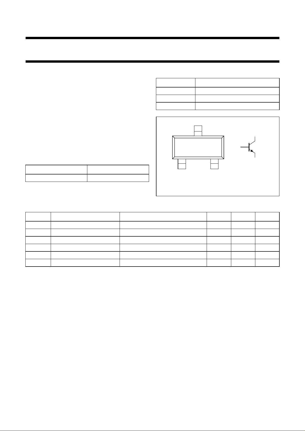
handbook, halfpage
DESCRIPTION
NPN transistor in a SOT23 plastic package.
MARKING
3
1
21
3
2
TYPE NUMBER MARKING CODE
BCF81 K9p
Top view
MAM255
Fig.1 Simplified outline (SOT23) and symbol.
QUICK REFERENCE DATA
SYMBOL PARAMETER CONDITIONS MIN. MAX. UNIT
V
V
I
P
h
f
CBO
CEO
CM
tot
FE
T
collector-base voltage open emitter − 50 V
collector-emitter voltage open base − 45 V
peak collector current − 200 mA
total power dissipation T
≤ 25 °C − 250 mW
amb
DC current gain IC= 2 mA; VCE= 5 V 420 800
transition frequency IC= 10 mA; VCE= 5 V; f = 100 MHz 100 − MHz
1997 Sep 03 2
Philips Semiconductors Product specification
NPN general purpose transistor BCF81
LIMITING VALUES
In accordance with the Absolute Maximum Rating System (IEC 134).
SYMBOL PARAMETER CONDITIONS MIN. MAX. UNIT
V
CBO
V
CEO
V
EBO
I
C
I
CM
I
BM
P
tot
T
stg
T
j
T
amb
Note
1. Transistor mounted on an FR4 printed-circuit board.
collector-base voltage open emitter − 50 V
collector-emitter voltage open base − 45 V
emitter-base voltage open collector − 5V
collector current (DC) − 100 mA
peak collector current − 200 mA
peak base current − 100 mA
total power dissipation T
≤ 25 °C; note 1 − 250 mW
amb
storage temperature −65 +150 °C
junction temperature − 150 °C
operating ambient temperature −65 +150 °C
THERMAL CHARACTERISTICS
SYMBOL PARAMETER CONDITIONS VALUE UNIT
R
th j-a
thermal resistance from junction to ambient note 1 500 K/W
Note
1. Transistor mounted on an FR4 printed-circuit board.
CHARACTERISTICS
=25°C unless otherwise specified.
T
j
SYMBOL PARAMETER CONDITIONS MIN. TYP. MAX. UNIT
I
CBO
I
EBO
h
FE
V
CEsat
V
BEsat
V
BE
C
c
f
T
F noise figure I
collector cut-off current IE= 0; VCB=20V −−100 nA
= 0; VCB= 20 V; Tj= 100 °C −−10 µA
I
E
emitter cut-off current IC= 0; VEB=5V −−100 nA
DC current gain IC= 2 mA; VCE= 5 V 420 − 800
collector-emitter saturation voltage IC= 10 mA; IB= 0.5 mA − 120 250 mV
= 50 mA; IB= 2.5 mA − 210 − mV
I
C
base-emitter saturation voltage IC= 10 mA; IB= 0.5 mA − 750 − mV
I
= 50 mA; IB= 2.5 mA − 850 − mV
C
base-emitter voltage IC= 2 mA; VCE= 5 V 550 − 700 mV
collector capacitance IE=ie= 0; VCB= 10 V; f = 1 MHz − 2.5 − pF
transition frequency IC= 10 mA; VCE= 5 V; f = 100 MHz 100 −−MHz
= 200 µA; VCE=5V; RS=2kΩ;
C
− 1.2 4 dB
f = 1 kHz; B = 200 Hz
1997 Sep 03 3
 Loading...