

Philips BC517 Datasheet
DISCRETE SEMICONDUCTORS
DATA SH EET
ook, halfpage
M3D186
BC517
NPN Darlington transistor
Product specification
Supersedes data of 1997 Apr 23
1999 Apr 23
Philips Semiconductors Product specification
NPN Darlington transistor BC517
FEATURES
• High current (max. 500 mA)
• Low voltage (max. 30 V)
• Very high DC current gain (min. 30000).
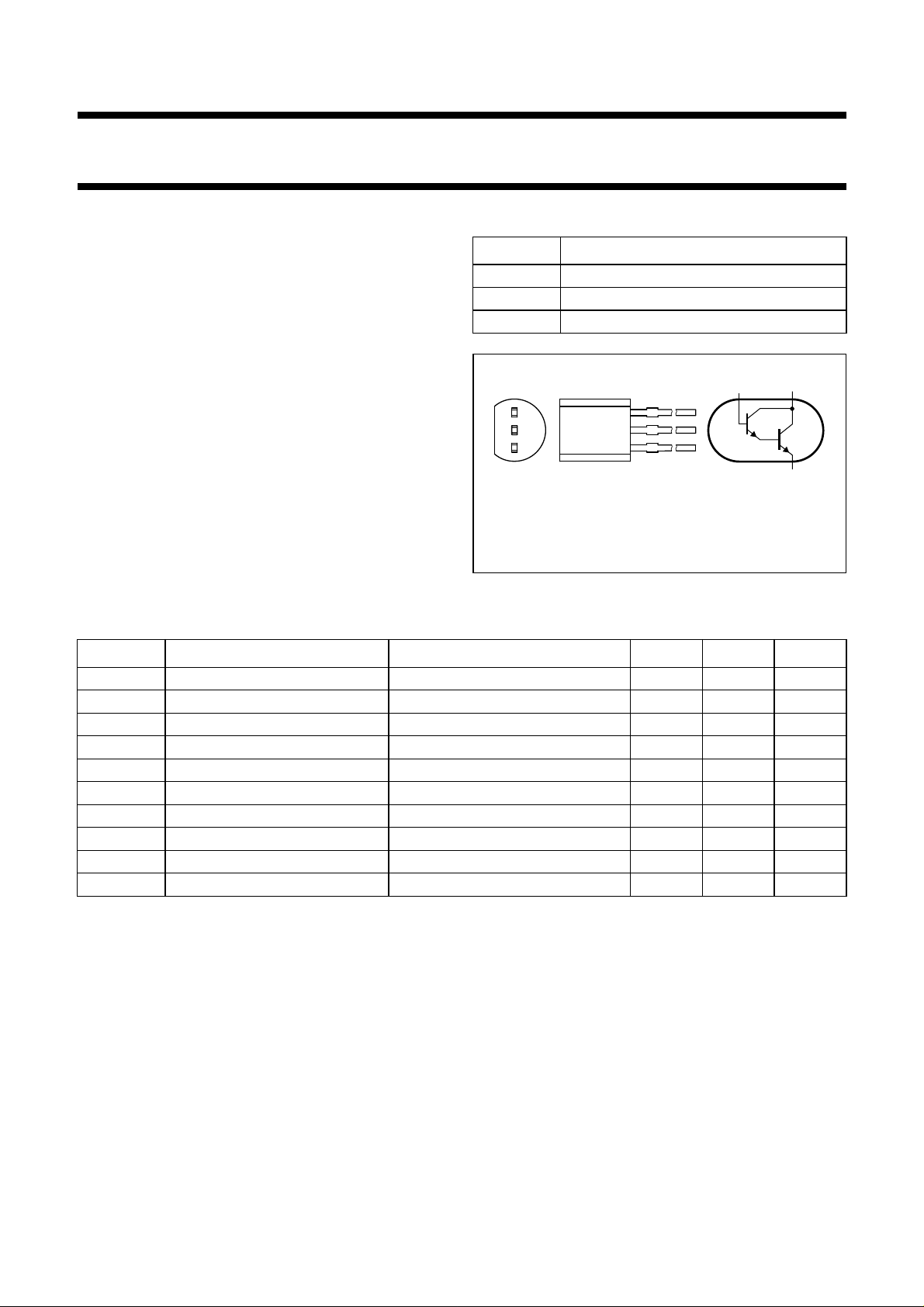
PINNING
PIN DESCRIPTION
1 emitter
2 base
3 collector
APPLICATIONS
• Where very high amplification is required.
23
TR1
TR2
DESCRIPTION
NPN Darlington transistor in a TO-92; SOT54 plastic
handbook, halfpage
1
2
3
package. PNP complement: BC516.
1
MAM302
Fig.1 Simplified outline (TO-92; SOT54)
and symbol.
LIMITING VALUES
In accordance with the Absolute Maximum Rating System (IEC 134).
SYMBOL PARAMETER CONDITIONS MIN. MAX. UNIT
V
V
V
I
I
I
P
T
T
T
CBO
CES
EBO
C
CM
B
tot
stg
j
amb
collector-base voltage open emitter − 40 V
collector-emitter voltage VBE=0 − 30 V
emitter-base voltage open collector − 10 V
collector current (DC) − 500 mA
peak collector current − 800 mA
base current (DC) − 100 mA
total power dissipation T
≤ 25 °C; note 1 − 500 mW
amb
storage temperature −65 +150 °C
junction temperature − 150 °C
operating ambient temperature −65 +150 °C
Note
1. Transistor mounted on an FR4 printed-circuit board.
1999 Apr 23 2
Philips Semiconductors Product specification
NPN Darlington transistor BC517
THERMAL CHARACTERISTICS
SYMBOL PARAMETER CONDITIONS VALUE UNIT
R
th j-a
Note
1. Transistor mounted on an FR4 printed-circuit board.
CHARACTERISTICS
=25°C unless otherwise specified.
T
j
SYMBOL PARAMETER CONDITIONS MIN. TYP. MAX. UNIT
I
CBO
I
EBO
h
FE
V
CEsat
V
BEsat
V
BEon
f
T
thermal resistance from junction to ambient note 1 250 K/W
collector cut-off current IE= 0; VCB=30V −−100 nA
emitter cut-off current IC= 0; VEB=10V −−100 nA
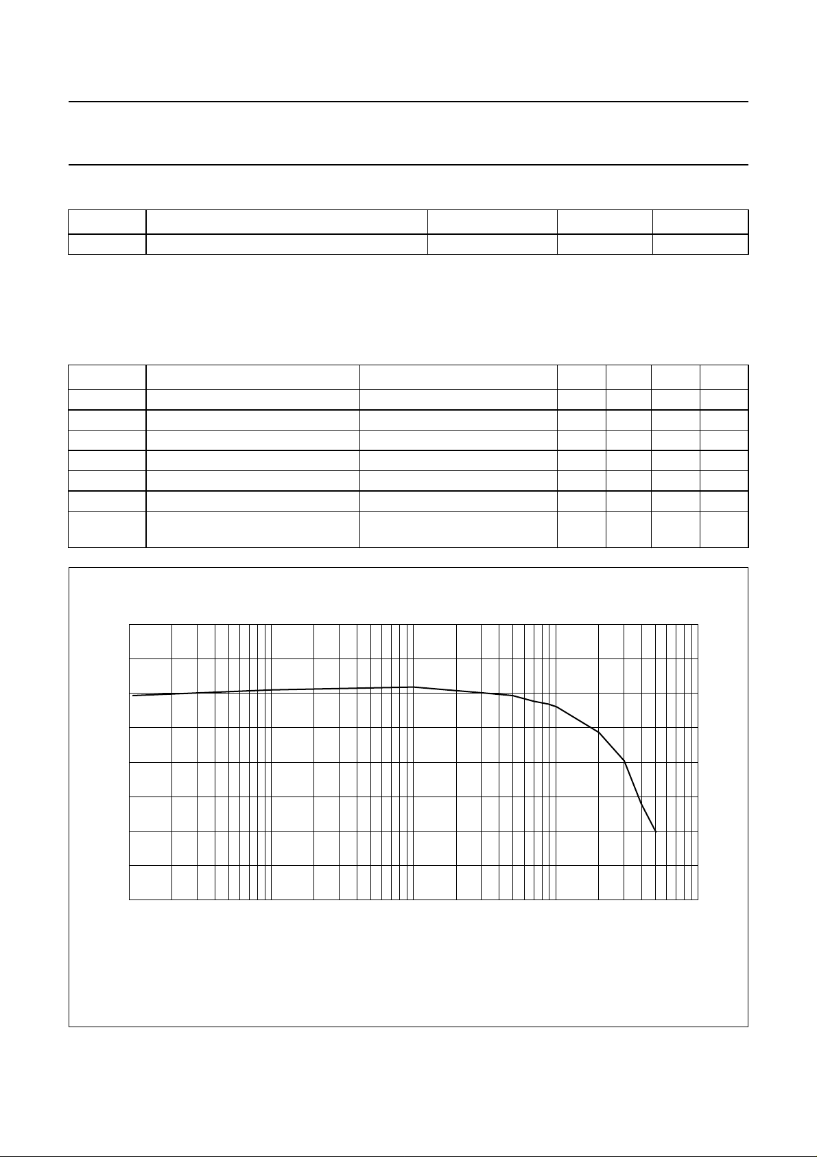
DC current gain IC= 20 mA; VCE= 2 V; see Fig.2 30000 −−
collector-emitter saturation voltage IC= 100 mA; IB= 0.1 mA −−1V
base-emitter saturation voltage IC= 100 mA; IB= 0.1 mA −−1.5 V
base-emitter on-state voltage IC= 10 mA; VCE=5V −−1.4 V
transition frequency IC= 30 mA; VCE=5V;
− 220 − MHz
f = 100 MHz
80000
handbook, full pagewidth
h
FE
60000
40000
20000
0
−1
10
VCE=2V.
1
10 10
Fig.2 DC current gain; typical values.
MGD837
2
IC (mA)
3
10
1999 Apr 23 3
 Loading...