

Philips BAX18 Datasheet
DISCRETE SEMICONDUCTORS
DATA SH EET
M3D176
BAX18
General purpose diode
Product specification
Supersedes data of April 1996
1996 Sep 18
Philips Semiconductors Product specification
General purpose diode BAX18
FEATURES
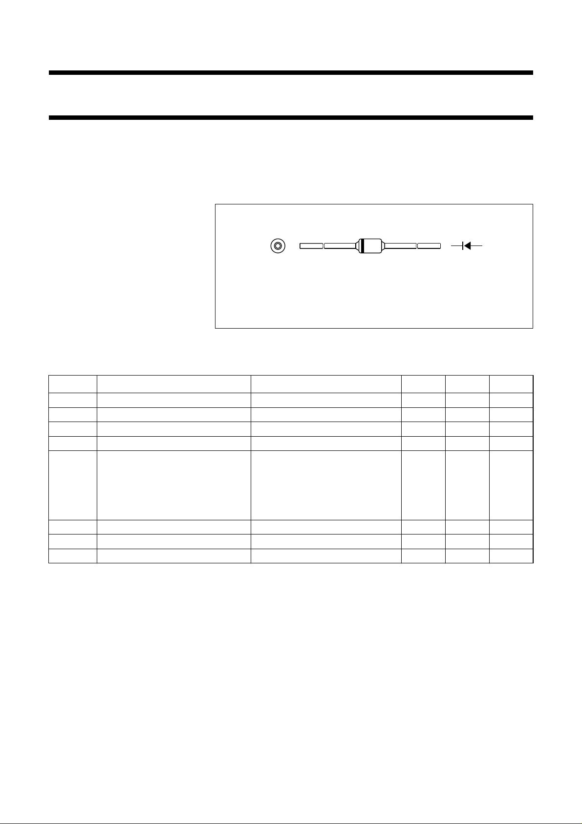
• Hermetically sealed leaded glass
SOD27 (DO-35) package
• Switching speed: max. 50 ns
DESCRIPTION
The BAX18 is a general purpose diode fabricated in planar technology, and
encapsulated in the hermetically sealed leaded glass SOD27 (DO-35)
package.
• General application
• Continuous reverse voltage:
max. 75 V
• Repetitive peak reverse voltage:
handbook, halfpage
k
a
max. 75 V
• Repetitive peak forward current:
MAM246
max. 2 A.
The diode is type branded.
APPLICATIONS
Fig.1 Simplified outline (SOD27; DO-35) and symbol.
• Rectifier applications.
LIMITING VALUES
In accordance with the Absolute Maximum Rating System (IEC 134).
SYMBOL PARAMETER CONDITIONS MIN. MAX. UNIT
V
V
I
F
I
FRM
I
FSM
RRM
R
repetitive peak reverse voltage − 75 V
continuous reverse voltage − 75 V
continuous forward current see Fig.2; note 1 − 500 mA
repetitive peak forward current − 2000 mA
non-repetitive peak forward current square wave; Tj=25°C prior to
surge; see Fig.4
t=1µs − 55 A
t = 100 µs − 15 A
t = 10 ms − 9A
P
tot
T
stg
T
j
total power dissipation T
=25°C; note 1 − 450 mW
amb
storage temperature −65 +200 °C
junction temperature − 200 °C
Note
1. Device mounted on an FR4 printed circuit-board; lead length 10 mm.
1996 Sep 18 2

Philips Semiconductors Product specification
General purpose diode BAX18
ELECTRICAL CHARACTERISTICS
T
=25°C; unless otherwise specified.
j
SYMBOL PARAMETER CONDITIONS MIN. MAX. UNIT
V
F
I
R
C
d
t
rr
THERMAL CHARACTERISTICS
forward voltage see Fig.3
I
= 300 mA − 1.0 V
F
I
= 2 A; Tj= 150 °C − 1.5 V
F
reverse current see Fig.5
V
=75V − 5 µA
R
V
=75V; Tj= 150 °C − 100 µA
R
diode capacitance f = 1 MHz; VR= 0; see Fig.6 − 35 pF
reverse recovery time when switched from IF= 30 mA to
− 50 ns
IR= 30 mA; RL= 100 Ω;
measured at IR= 3 mA; see Fig.7
SYMBOL PARAMETER CONDITIONS VALUE UNIT
R
R
th j-tp
th j-a
thermal resistance from junction to tie-point lead length 10 mm 240 K/W
thermal resistance from junction to ambient lead length 10 mm; note 1 375 K/W
Note
1. Device mounted on a printed circuit-board without metallization pad.
1996 Sep 18 3
 Loading...