

Philips BAV199W Datasheet
DISCRETE SEMICONDUCTORS
DATA SH EET
ook, halfpage
M3D102
BAV199W
Low-leakage double diode
Product specification
Supersedes data of 1998 Jan 09
1999 May 11
Philips Semiconductors Product specification
Low-leakage double diode BAV199W
FEATURES
• Small plastic SMD package
• Low leakage current: typ. 3 pA
• Switching time: typ. 0.8 µs
• Continuous reverse voltage:
max. 75 V
• Repetitive peak reverse voltage:
max. 85 V
• Repetitive peak forward current:
max. 500 mA.
APPLICATIONS
• Low-leakage current applications in
surface mounted circuits.
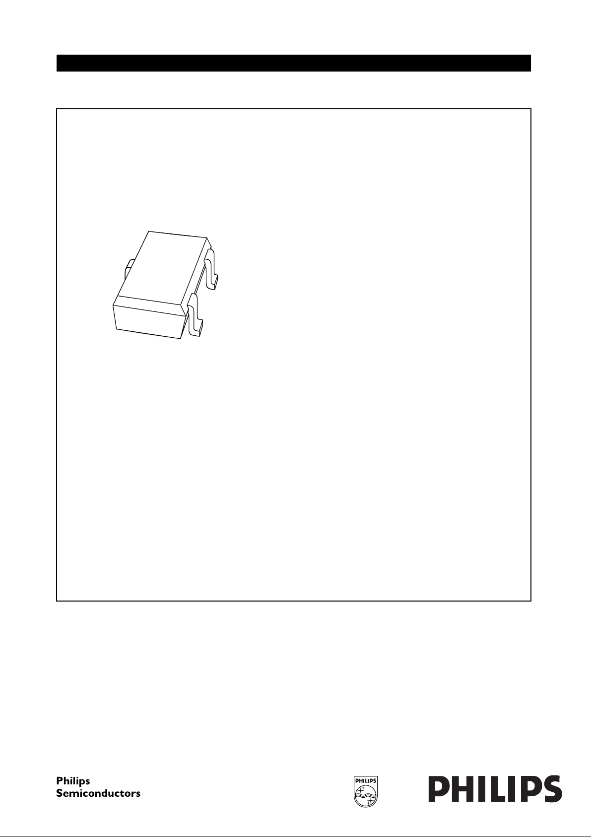
DESCRIPTION
Epitaxial, medium-speed switching,
double diode in a small plastic
SOT323 (SC-70) SMD package.
The diodes are connected in series.
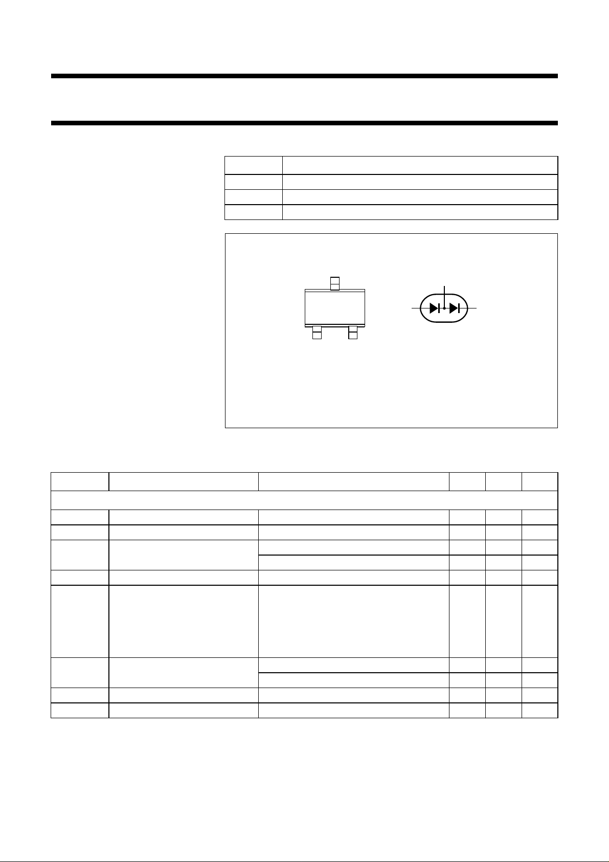
PINNING
PIN DESCRIPTION
1 anode
2 cathode
3 cathode; anode
handbook, halfpage
12
Top view
Marking code: JY- =made in Hong Kong; JYt = made in Malaysia.
3
MAM391
Fig.1 Simplified outline (SOT323; SC-70) and symbol.
3
21
LIMITING VALUES
In accordance with the Absolute Maximum Rating System (IEC 134).
SYMBOL PARAMETER CONDITIONS MIN. MAX. UNIT
Per diode unless otherwise specified
V
V
I
F
I
FRM
I
FSM
P
T
T
RRM
R
tot
stg
j
repetitive peak reverse voltage − 85 V
continuous reverse voltage − 75 V
continuous forward current single diode loaded; Ts=90°C; see Fig.2 − 135 mA
double diode loaded; T
=90°C; see Fig.2 − 110 mA
s
repetitive peak forward current − 500 mA
non-repetitive peak forward
current
square wave; Tj=25°C prior to surge;
see Fig.4
t
=1µs − 4A
p
=1ms − 1A
t
p
=1s − 0.5 A
t
p
total power dissipation single diode loaded; Ts=90°C − 150 mW
double diode loaded; T
=90°C − 240 mW
s
storage temperature −65 +150 °C
junction temperature − 150 °C
1999 May 11 2

Philips Semiconductors Product specification
Low-leakage double diode BAV199W
ELECTRICAL CHARACTERISTICS
T
= 25°C unless otherwise specified.
j
SYMBOL PARAMETER CONDITIONS TYP. MAX. UNIT
Per diode
V
F
I
R
C
d
t
rr
forward voltage see Fig.3
=1mA − 900 mV
I
F
I
=10mA − 1000 mV
F
=50mA − 1100 mV
I
F
I
= 150 mA − 1250 mV
F
reverse current see Fig.5
V
= 75 V 0.003 5 nA
R
= 75 V; Tj= 150 °C 3 80 nA
V
R
diode capacitance f = 1 MHz; VR= 0; see Fig.6 2 − pF
reverse recovery time when switched from IF= 10 mA to
0.8 3 µs
IR= 10 mA; RL= 100 Ω;
measured at IR= 1 mA; see Fig.7
THERMAL CHARACTERISTICS
SYMBOL PARAMETER CONDITIONS VALUE UNIT
R
th j-s
thermal resistance from junction to soldering point Ts=90°C 400 K/W
1999 May 11 3
 Loading...