

Philips BAV105 Datasheet
DISCRETE SEMICONDUCTORS
DATA SH EET
1/3 page (Datasheet)
M3D054
BAV105
High-speed diode
Product specification
Supersedes data of April 1996
1996 Sep 17
Philips Semiconductors Product specification
High-speed diode BAV105
FEATURES
• Small hermetically sealed glass
SMD package
• High switching speed: max. 6 ns
DESCRIPTION
The BAV105 is a high-speed switching diode fabricated in planar technology,
and encapsulated in the small hermetically sealed glass SOD80C SMD
package.
• General application
• Continuous reverse voltage:
max. 60 V
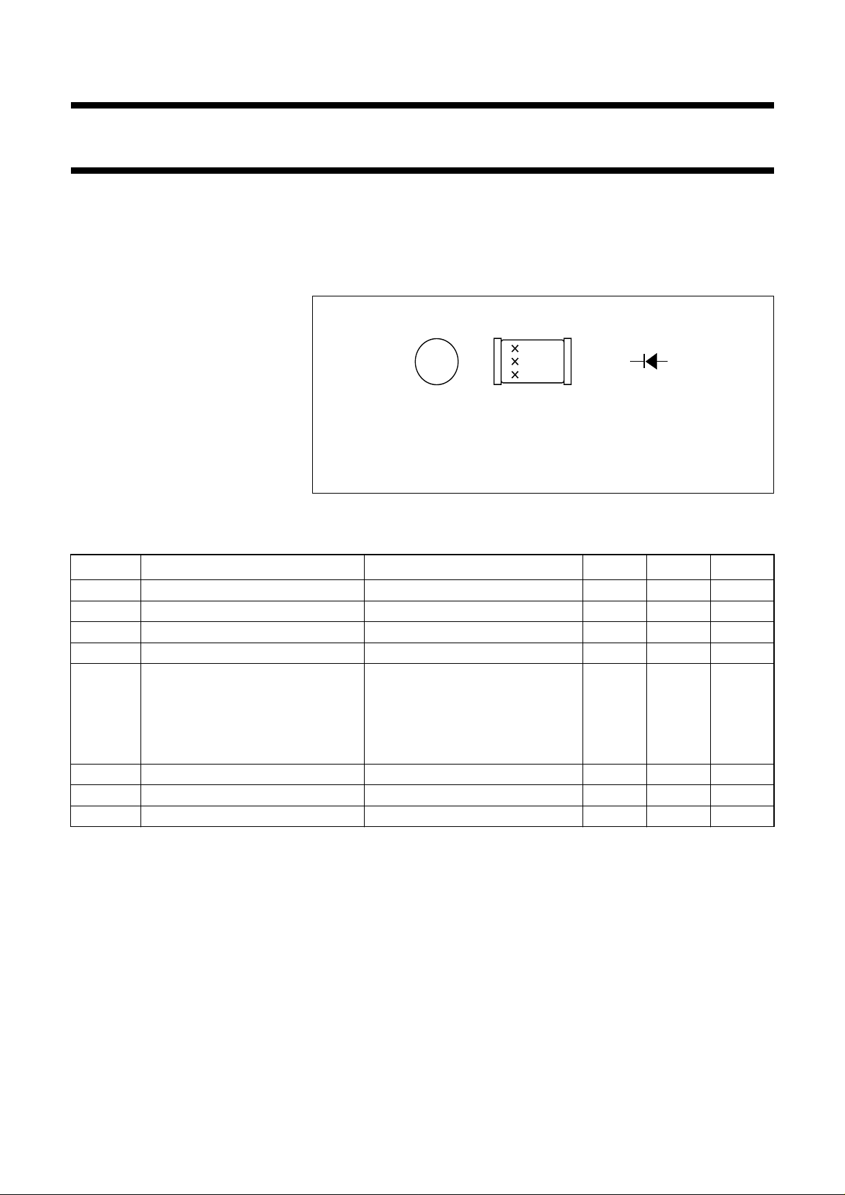
handbook, 4 columns
ka
• Repetitive peak reverse voltage:
max. 60 V
• Repetitive peak forward current:
MAM061
max. 600 mA.
APPLICATIONS
• High-speed switching in e.g.
Cathode indicated by black band.
Fig.1 Simplified outline (SOD80C) and symbol.
surface mounted circuits.
LIMITING VALUES
In accordance with the Absolute Maximum Rating System (IEC 134).
SYMBOL PARAMETER CONDITIONS MIN. MAX. UNIT
V
V
I
F
I
FRM
I
FSM
RRM
R
repetitive peak reverse voltage − 60 V
continuous reverse voltage − 60 V
continuous forward current see Fig.2; note 1 − 300 mA
repetitive peak forward current − 600 mA
non-repetitive peak forward current square wave; Tj=25°C prior to
surge; see Fig.4
t=1µs − 9A
t = 100 µs − 3A
t=1s − 1A
P
tot
T
stg
T
j
total power dissipation T
=25°C; note 1 − 500 mW
amb
storage temperature −65 +200 °C
junction temperature − 200 °C
Note
1. Device mounted on an FR4 printed-circuit board.
1996 Sep 17 2

Philips Semiconductors Product specification
High-speed diode BAV105
ELECTRICAL CHARACTERISTICS
T
=25°C; unless otherwise specified.
j
SYMBOL PARAMETER CONDITIONS MIN. MAX. UNIT
V
F
I
R
C
d
t
rr
V
fr
forward voltage see Fig.3
I
=10mA − 750 mV
F
I
= 200 mA − 1000 mV
F
= 500 mA − 1.25 V
I
F
I
= 200 mA; Tj= 100 °C − 950 mV
F
reverse current see Fig.5
=60V − 100 nA
V
R
V
= 60 V; Tj= 150 °C − 100 µA
R
diode capacitance f = 1 MHz; VR= 0; see Fig.6 − 2.5 pF
reverse recovery time when switched from IF= 400 mA to
− 6ns
IR= 400 mA; RL= 100 Ω; measured at
IR= 40 mA; see Fig.7
forward recovery voltage when switched from IF= 400 mA;
− 2V
tr1= 30 ns; see Fig.8
when switched from I
= 400 mA;
F
− 1.5 V
tr2= 100 ns; see Fig.8
THERMAL CHARACTERISTICS
SYMBOL PARAMETER CONDITIONS VALUE UNIT
R
R
th j-tp
th j-a
thermal resistance from junction to tie-point 300 K/W
thermal resistance from junction to ambient note 1 350 K/W
Note
1. Device mounted on an FR4 printed-circuit board.
1996 Sep 17 3
 Loading...