

Philips BAT74S Datasheet
DISCRETE SEMICONDUCTORS
DATA SH EET
alfpage
MBD128
BAT74S
Schottky barrier double diode
Product specification
Supersedes data of 1998 Feb 06
1998 Jul 10
Philips Semiconductors Product specification
Schottky barrier double diode BAT74S
FEATURES
• Low forward voltage
• Guard ring protected
• Small SMD package.
APPLICATIONS
• Ultra high-speed switching
• Voltage clamping
• Protection circuits
• Blocking diodes.
DESCRIPTION
Planar Schottky barrier double diode
with an integrated guard ring for
stress protection.
Two separate dies are encapsulated
in a SOT363 small SMD plastic
package.
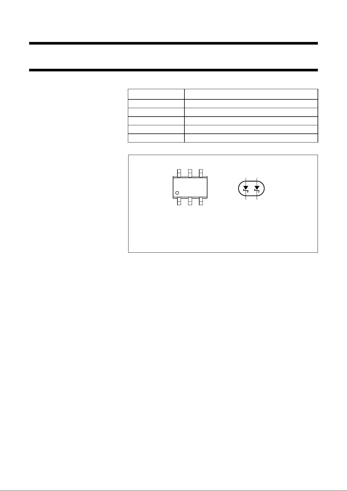
PINNING
Marking code: 74.
PIN DESCRIPTION
1 anode (a
)
1
2,5 not connected
3 cathode (k
4 anode (a
6 cathode (k
654
123
Top view
)
2
)
2
)
1
handbook, 2 columns
MSA370
14
63
MBK149
Fig.1 Simplified outline (SOT363) and symbol.
1998 Jul 10 2

Philips Semiconductors Product specification
Schottky barrier double diode BAT74S
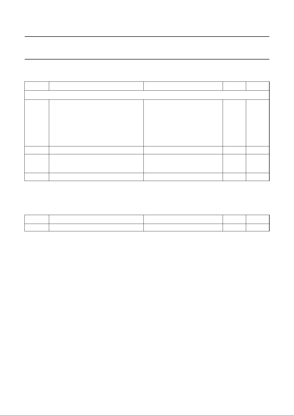
LIMITING VALUES
In accordance with the Absolute Maximum Rating System (IEC 134).
SYMBOL PARAMETER CONDITIONS MIN. MAX. UNIT
Per diode
V
I
F
I
FRM
I
FSM
P
T
T
T
R
tot
stg
j
amb
continuous reverse voltage
continuous forward current −
repetitive peak forward current tp≤ 1s;δ≤0.5
non-repetitive peak forward current tp< 10 ms 600 mA
total power dissipation
storage temperature
junction temperature
operating ambient temperature
Double diode operation
V
V
I
F
I
FRM
R
R
continuous reverse voltage
continuous reverse voltage
continuous forward current −
repetitive peak forward current tp≤ 1s;δ≤0.5
≤ 25 °C; see Fig.2
T
amb
series connection −
−
−
−
−65
−
−65
−
−
30 V
200 mA
300 mA
230 mW
+150 °C
125 °C
+125 °C
30 V
60 V
(1)
110
mA
200 mA
Note
1. If both diodes are in forward operation at the same moment, total device current is max. 110 mA. If one diode is in
reverse and the other in forward operation at the same moment, total device current is max. 200 mA.
1998 Jul 10 3
Philips Semiconductors Product specification
Schottky barrier double diode BAT74S
ELECTRICAL CHARACTERISTICS
T
=25°C unless otherwise specified.
amb
SYMBOL PARAMETER CONDITIONS MAX. UNIT
Per diode
V
F
I
R
t
rr
C
d
forward voltage see Fig.3
= 0.1 mA
I
F
I
=1mA
F
I
=10mA
F
I
=30mA
F
I
= 100 mA
F
reverse current VR= 25 V; note 1; see Fig.4
reverse recovery time when switched from IF= 10 mA to
IR= 10 mA; RL= 100 Ω;
measured at IR=1mA
diode capacitance f = 1 MHz; VR= 1 V; see Fig.5
240 mV
320 mV
400 mV
500 mV
800 mV
2
µA
5ns
10 pF
Note
1. Pulsed test: t
= 300 µs; δ = 0.02.
p
THERMAL CHARACTERISTICS
SYMBOL PARAMETER CONDITIONS VALUE UNIT
R
th j-a
thermal resistance from junction to ambient note 1 416 K/W
Note
1. Refer to SOT363 standard mounting conditions.
1998 Jul 10 4
 Loading...