

Philips BAT54C, BAT54 Datasheet
DISCRETE SEMICONDUCTORS
DATA SH EET
ok, halfpage
M3D088
BAT54 series
Schottky barrier (double) diodes
Product specification
Supersedes data of 1996 Mar 19
1999 May 06
Philips Semiconductors Product specification
Schottky barrier (double) diodes BAT54 series
FEATURES
• Low forward voltage
• Guard ring protected
• Small plastic SMD package.
APPLICATIONS
• Ultra high-speed switching
• Voltage clamping
• Protection circuits
• Blocking diodes.
DESCRIPTION
Planar Schottky barrier diodes
encapsulated in a SOT23 small
plastic SMD package. Single diodes
and double diodes with different
pinning are available.
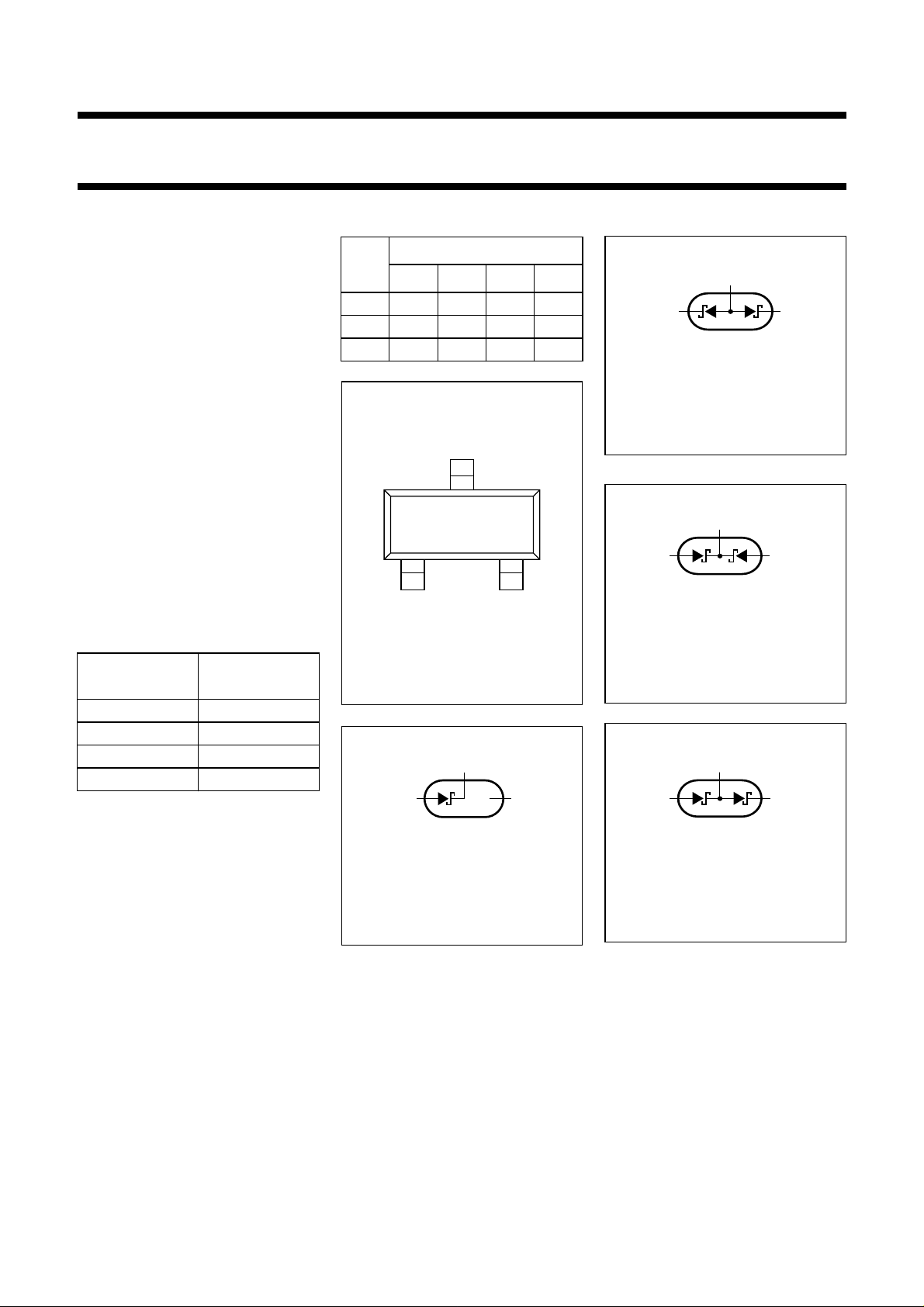
MARKING
TYPE NUMBER
MARKING
(1)
CODE
BAT54 L4∗
BAT54A L42
BAT54C L43
BAT54S L44
Note
1. ∗ = p : Made in Hong Kong.
∗ = t : Made in Malaysia.
PINNING
BAT54
PIN
ACS
1ak
2 n.c. k
3ka
handbook, 2 columns
Top view
1
2
1,a2k1,k2k1,a2
Fig.1 Simplified outline
(SOT23) and pin
configuration.
3
12
3
MLC357
a
1
a
2
21
MGC421
n.c.
a
1
k
2
3
12
MLC360
Fig.3 BAT54A diode
configuration (symbol).
3
12
MLC359
Fig.4 BAT54C diode
configuration (symbol).
3
12
MLC358
Fig.2 BAT54 single diode
configuration (symbol).
1999 May 06 2
Fig.5 BAT54S diode
configuration (symbol).
Philips Semiconductors Product specification
Schottky barrier (double) diodes BAT54 series
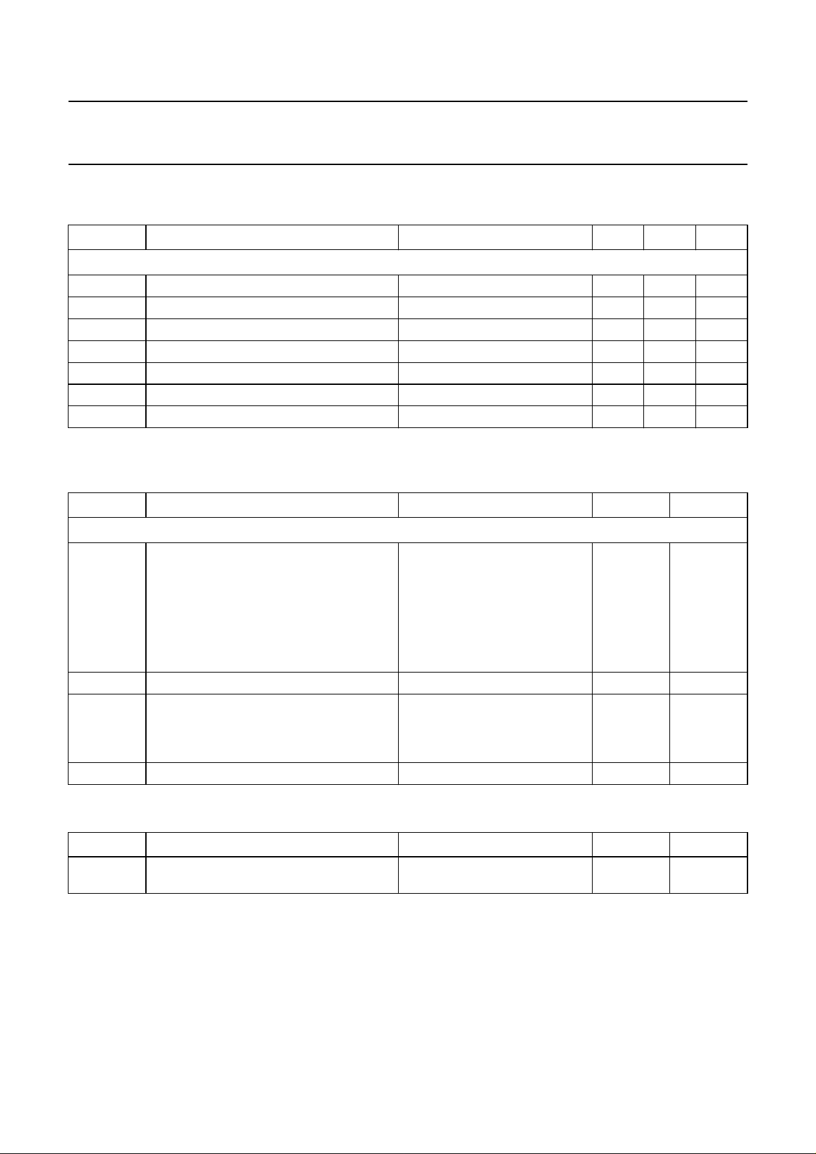
LIMITING VALUES
In accordance with the Absolute Maximum Rating System (IEC 134).
SYMBOL PARAMETER CONDITIONS MIN. MAX. UNIT
Per diode
V
R
I
F
I
FRM
I
FSM
P
tot
T
stg
T
j
ELECTRICAL CHARACTERISTICS
T
=25°C unless otherwise specified.
amb
continuous reverse voltage
continuous forward current −
repetitive peak forward current tp≤ 1s;δ≤0.5
non-repetitive peak forward current tp<10ms
≤ 25 °C
total power dissipation (per package)
T
amb
storage temperature
junction temperature
−
−
−
−
−65
−
30 V
200 mA
300 mA
600 mA
230 mW
+150 °C
125 °C
SYMBOL PARAMETER CONDITIONS MAX. UNIT
Per diode
V
F
I
R
t
rr
forward voltage see Fig.6
I
= 0.1 mA
F
=1mA
I
F
I
=10mA
F
I
=30mA
F
I
= 100 mA
F
reverse current VR= 25 V; see Fig.7
reverse recovery time when switched from IF=10mA
240 mV
320 mV
400 mV
500 mV
800 mV
2
µA
5ns
to IR= 10 mA; RL= 100 Ω;
measured at IR= 1 mA;
see Fig.9
C
d
diode capacitance f = 1 MHz; VR= 1 V; see Fig.8
10 pF
THERMAL CHARACTERISTICS
SYMBOL PARAMETER CONDITIONS VALUE UNIT
R
th j-a
thermal resistance from junction to
note 1 500 K/W
ambient
Note
1. Refer to SOT23 standard mounting conditions.
1999 May 06 3
 Loading...