

Philips BAT254 Datasheet
DISCRETE SEMICONDUCTORS
DATA SH EET
book, halfpage
M3D154
BAT254
Schottky barrier diode
Product specification
Supersedes data of 1996 Mar 19
1999 Apr 22
Philips Semiconductors Product specification
Schottky barrier diode BAT254
FEATURES
• Low forward voltage
• Guard ring protected
DESCRIPTION
Planar Schottky barrier diode encapsulated in a SOD110 very small ceramic
SMD package.
• Very small ceramic SMD package.
APPLICATIONS
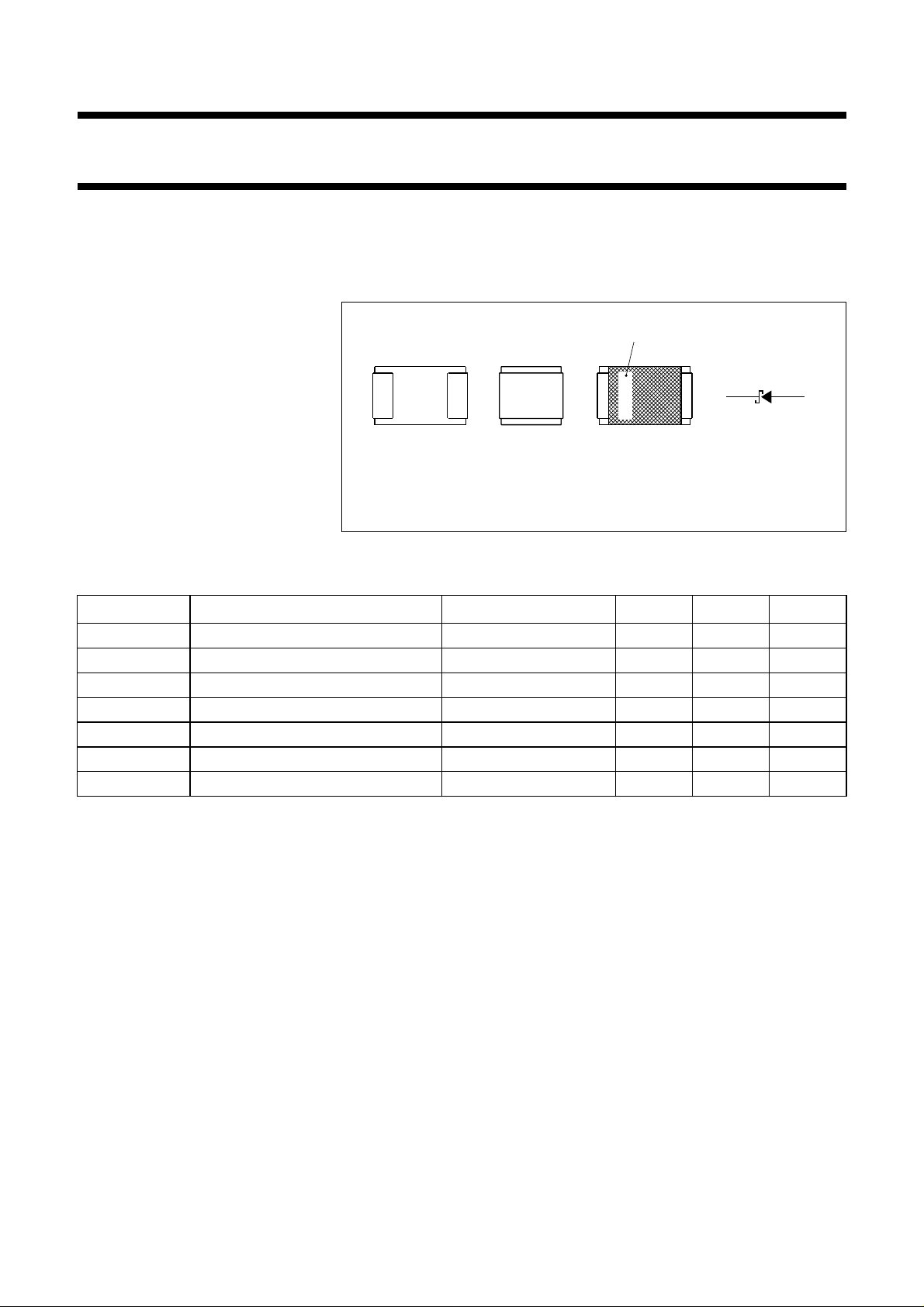
handbook, 4 columns
ak
cathode mark
ka
• Ultra high-speed switching
• Voltage clamping
• Protection circuits
• Blocking diodes.
top viewside viewbottom view
Marking code: L4.
MAM214
Fig.1 Simplified outline (SOD110) and symbol.
LIMITING VALUES
In accordance with the Absolute Maximum Rating System (IEC 134).
SYMBOL PARAMETER CONDITIONS MIN. MAX. UNIT
V
I
F
I
FRM
I
FSM
T
T
T
R
stg
j
amb
continuous reverse voltage
continuous forward current −
repetitive peak forward current tp≤ 1s;δ≤0.5
non-repetitive peak forward current tp< 10 ms
storage temperature
junction temperature
operating ambient temperature
−
−
−
−65
−
−65
30 V
200 mA
300 mA
600 mA
+150 °C
125 °C
+125 °C
1999 Apr 22 2

Philips Semiconductors Product specification
Schottky barrier diode BAT254
ELECTRICAL CHARACTERISTICS
T
=25°C unless otherwise specified.
amb
SYMBOL PARAMETER CONDITIONS MAX. UNIT
V
F
I
R
t
rr
C
d
forward voltage see Fig.2
= 0.1 mA
I
F
I
= 1mA
F
=10mA
I
F
I
=30mA
F
I
= 100 mA
F
reverse current VR= 25 V; note 1; see Fig.3
reverse recovery time when switched from IF= 10 mA to
IR= 10 mA; RL= 100 Ω; measured at
IR= 1 mA: see Fig.5
diode capacitance f = 1 MHz; VR= 1 V; see Fig.4
240 mV
320 mV
400 mV
500 mV
800 mV
2
µA
5ns
10 pF
Note
1. Pulse test: t
= 300 µs; δ = 0.02.
p
THERMAL CHARACTERISTICS
SYMBOL PARAMETER CONDITIONS VALUE UNIT
R
th j-a
thermal resistance from junction to ambient note 1 315 K/W
Note
1. Refer to SOD110 standard mounting conditions.
1999 Apr 22 3
 Loading...