

Philips bat160 DATASHEETS
DISCRETE SEMICONDUCTORS
DATA SH EET
halfpage
M3D087
BAT160 series
Schottky barrier double diodes
Product specification
Supersedes data of 1999 Mar 26
1999 Sep 20
Philips Semiconductors Product specification
Schottky barrier double diodes BAT160 series
FEATURES
• Low switching losses
• Capability of absorbing very high
surge current
• Fast recovery time
• Guard ring protected
• Plastic SMD package.
APPLICATIONS
• Low power switched-mode power
supplies
• Rectification
• Polarity protection.
DESCRIPTION
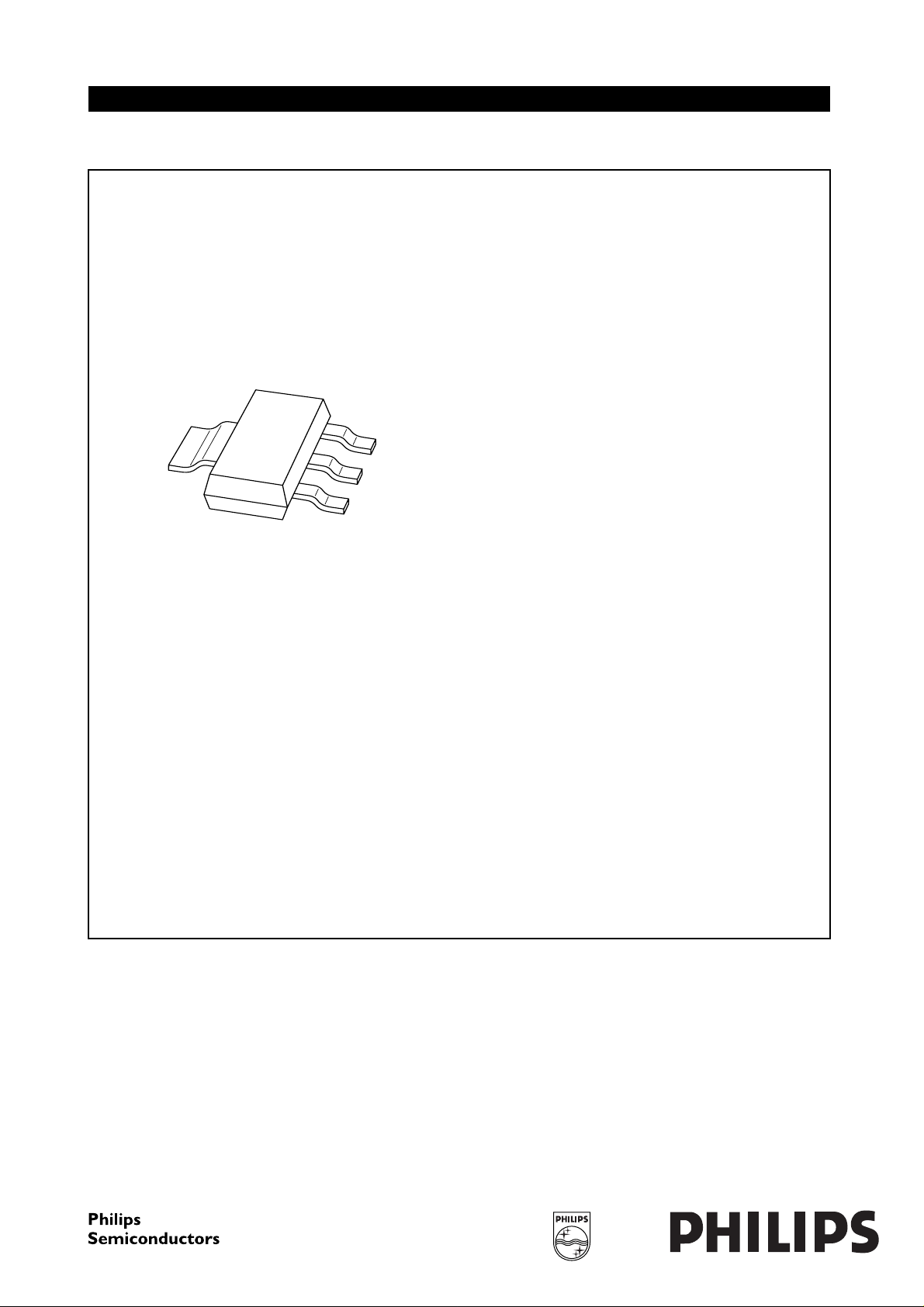
PlanarSchottkybarrierdoublediodes
encapsulated in a SOT223 plastic
SMD package.
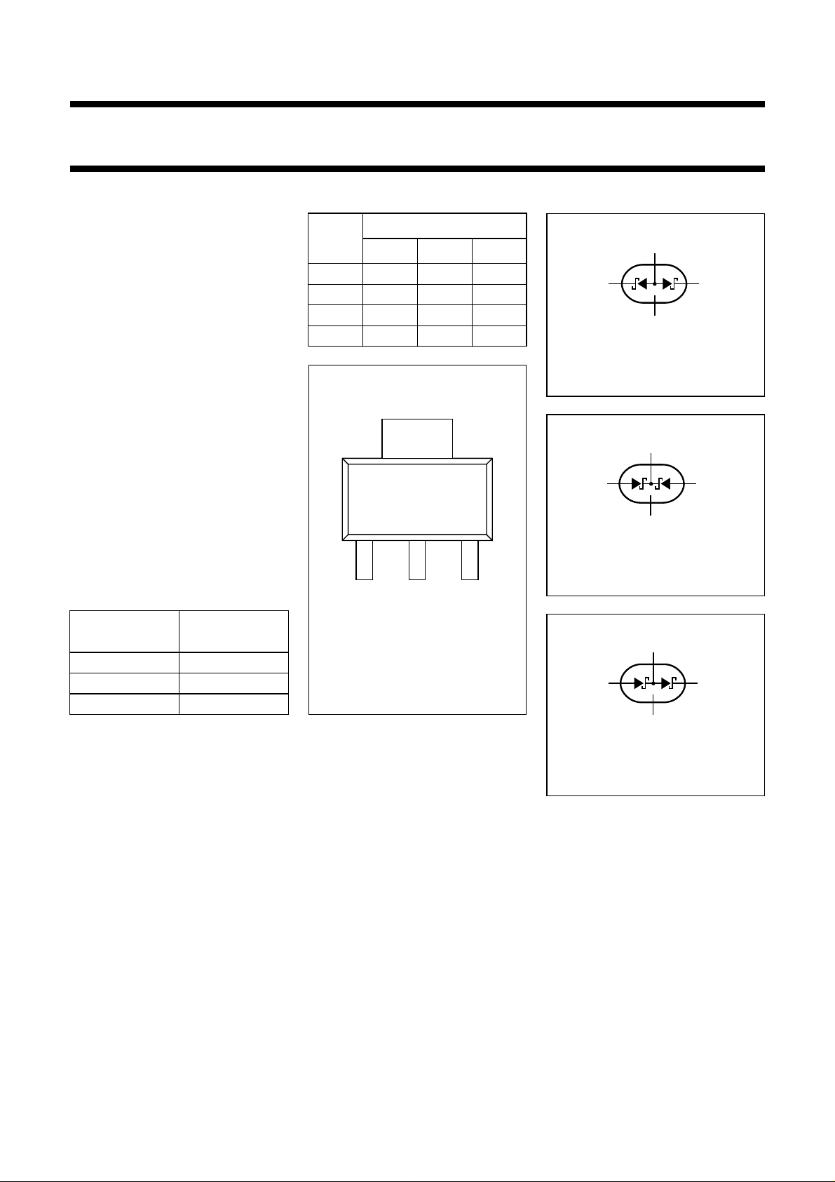
MARKING
PINNING
BAT160
PIN
ACS
1k
1
a
1
2 n.c. n.c. n.c.
3k
4a
ge
1
123
Top view
2
, a2k1, k
a
2
2
4
MSB002 - 1
a
1
k
2
k1, a
2
age
13
4
2 n.c.
Fig.2 BAT160A diode
configuration (symbol).
age
13
4
2 n.c.
Fig.3 BAT160C diode
configuration (symbol).
MGL171
MGL172
TYPE NUMBER
MARKING
CODE
BAT160A AT160A
BAT160C AT160C
BAT160S AT160S
Fig.1 Simplified outline
(SOT223) and pin
configuration.
age
13
4
2 n.c.
Fig.4 BAT160S diode
configuration (symbol).
MGL173
1999 Sep 20 2
Philips Semiconductors Product specification
Schottky barrier double diodes BAT160 series
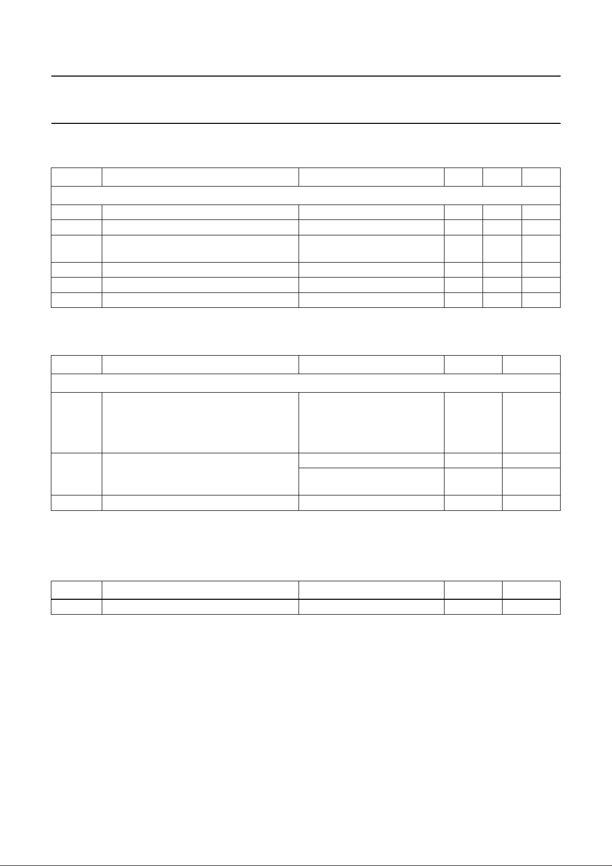
LIMITING VALUES
In accordance with the Absolute Maximum Rating System (IEC 134).
SYMBOL PARAMETER CONDITIONS MIN. MAX. UNIT
Per diode
V
R
I
F
I
FSM
I
RSM
T
stg
T
j
ELECTRICAL CHARACTERISTICS
T
=25°C unless otherwise specified.
amb
continuous reverse voltage − 60 V
continuous forward current − 1A
non-repetitive peak forward current tp= 8.3 ms; half sinewave;
− 10 A
JEDEC method
non-repetitive peak reverse current tp= 100 µs − 0.5 A
storage temperature −65 +150 °C
junction temperature − 150 °C
SYMBOL PARAMETER CONDITIONS MAX. UNIT
Per diode
V
F
I
R
forward voltage see Fig.5
= 100 mA 400 mV
I
F
I
= 1 A 650 mV
F
I
= 2 A 850 mV
F
reverse current VR= 60 V; note 1; see Fig.6 350 µA
V
= 60 V; Tj= 100 °C; note 1;
R
8mA
see Fig.6
C
d
diode capacitance f = 1 MHz; VR= 4 V; see Fig 7 60 pF
Note
1. Pulse test: t
= 300 µs; δ = 0.02.
p
THERMAL CHARACTERISTICS
SYMBOL PARAMETER CONDITIONS VALUE UNIT
R
th j-a
thermal resistance from junction to ambient note 1 100 K/W
Note
1. Refer to SOT223 standard mounting conditions.
1999 Sep 20 3
 Loading...