

Philips bat140 DATASHEETS
DISCRETE SEMICONDUCTORS
DATA SH EET
ok, halfpage
M3D087
BAT140 series
Schottky barrier double diodes
Product specification
File under Discrete Semiconductors, SC01
1997 Oct 03
Philips Semiconductors Product specification
Schottky barrier double diodes BAT140 series
FEATURES
• Low switching losses
• Capability of absorbing very high
surge current
• Fast recovery time
• Guard ring protected
• Plastic SMD package.
APPLICATIONS
• Low power switched-mode power
supplies
• Rectification
• Polarity protection.
DESCRIPTION
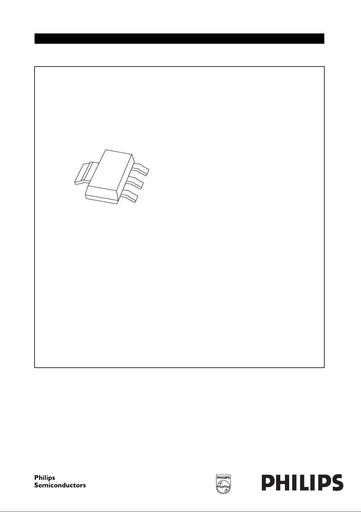
Planar Schottky barrier double diodes
encapsulated in a SOT223 plastic
SMD package.
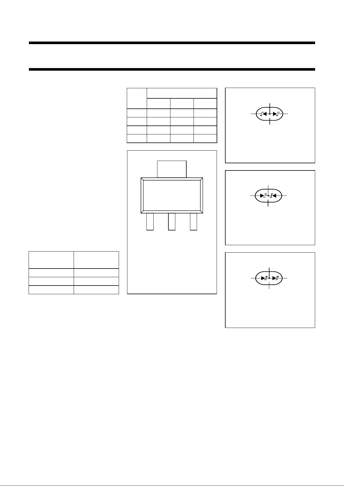
MARKING
PINNING
BAT140
PIN
ACS
1k
1
a
1
2 n.c. n.c. n.c.
3k
2
a
2
4a1,a2k1,k2k1,a
ge
123
Top view
4
MSB002 - 1
a
1
k
2
2
age
13
4
2 n.c.
Fig.2 BAT140A diode
configuration (symbol).
age
13
4
2 n.c.
Fig.3 BAT140C diode
configuration (symbol).
MGL171
MGL172
TYPE NUMBER
MARKING
BAT140A AT140A
BAT140C AT140C
BAT140S AT140S
CODE
Fig.1 Simplified outline
(SOT223) and pin
configuration.
age
13
4
2 n.c.
Fig.4 BAT140S diode
configuration (symbol).
MGL173
1997 Oct 03 2
Philips Semiconductors Product specification
Schottky barrier double diodes BAT140 series
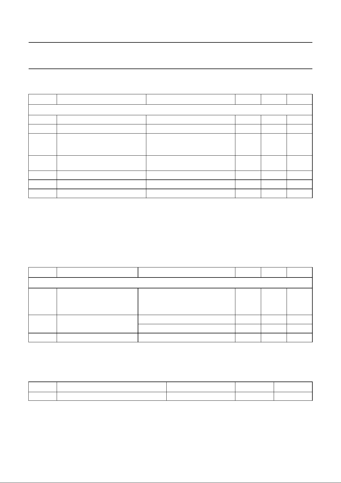
LIMITING VALUES
In accordance with the Absolute Maximum Rating System (IEC 134).
SYMBOL PARAMETER CONDITIONS MIN. MAX. UNIT
Per diode
V
R
I
F
I
F(AV)
I
FSM
I
RSM
T
stg
T
j
continuous reverse voltage
continuous forward current −
T
average forward current
=65°C;
amb
R
= 80 K/W; note 1;
th j-a
V
R(equiv)
= 0.2 V; note 2
non-repetitive peak forward current t = 8.3 µs half sinewave;
JEDEC method
non-repetitive peak reverse current tp= 100 µs
storage temperature
junction temperature
−
−
−
−
−65
−
40 V
1A
1A
10 A
0.5 A
+150 °C
125 °C
Notes
1. Refer to SOT223 standard mounting conditions.
2. For Schottky barrier diodes thermal run-away has to be considered, as in some applications, the reverse power
losses P
PR and I
are a significant part of the total power losses. Nomograms for determination of the reverse power losses
R
rating will be available on request.
F(AV)
ELECTRICAL CHARACTERISTICS
T
=25°C unless otherwise specified.
amb
SYMBOL PARAMETER CONDITIONS TYP. MAX. UNIT
Per diode
V
F
I
R
C
d
forward voltage see Fig.5
I
= 100 mA; note 1
F
I
= 1 A; note 1
F
reverse current VR= 10 V; note 1; see Fig.6
= 40 V; note 1; see Fig.6
V
R
diode capacitance VR= 4 V; f = 1 MHz; see Fig.7
280 330 mV
460 500 mV
15 40
60 300
µA
µA
65 80 pF
Note
1. Pulsed test: t
= 300 µs; δ = 0.02.
p
THERMAL CHARACTERISTICS
SYMBOL PARAMETER CONDITIONS VALUE UNIT
R
th j-a
thermal resistance from junction to ambient note 1 100 K/W
Note
1. Refer to SOT223 standard mounting conditions.
1997 Oct 03 3
 Loading...