

Philips 74lv04 DATASHEETS

INTEGRATED CIRCUITS
74LV04
Hex inverter
Product specification
Supersedes data of 1997 Feb 03
IC24 Data Handbook
1998 Apr 20
Philips Semiconductors Product specification
74L V04Hex inverter
FEA TURES
•Wide operating voltage: 1.0 to 5.5 V
•Optimized for low voltage applications: 1.0 to 3.6 V
•Accepts TTL input levels between V
•Typical V
T
amb
•Typical V
T
amb
(output ground bounce) < 0.8 V at V
OLP
= 25°C
(output VOH undershoot) > 2 V at V
OHV
= 25°C
= 2.7 V and V
CC
CC
CC
CC
= 3.3 V,
= 3.3 V,
•Output capability: standard
•I
category: SSI
CC
QUICK REFERENCE DATA
GND = 0 V; T
SYMBOL
t
NOTES:
is used to determine the dynamic power dissipation (PD in µW)
1. C
PD
P
= CPD V
D
= input frequency in MHz; CL = output load capacitance in pF;
f
i
f
= output frequency in MHz; VCC = supply voltage in V;
o
(C
L
2. The condition is V
= 25°C; tr = tf 2.5 ns
amb
PHL/tPLH
C
I
C
PD
CC
2
V
fo) = sum of the outputs.
CC
PARAMETER CONDITIONS TYPICAL UNIT
Propagation delay
nA to nY
Input capacitance 3.5 pF
Power dissipation capacitance per gate See Notes NO TAG and 2 21 pF
2
fi (CL V
is V1 = GND to V
1
2
fo) where:
CC
CC.
= 3.6 V
DESCRIPTION
The 74LV04 is a low-voltage Si-gate CMOS device that is pin and
function compatible with 74HC/HCT04.
The 74LV04 provides six inverting buffers.
CL = 15 pF;
VCC = 3.3 V
6 ns
ORDERING INFORMATION
PACKAGES TEMPERATURE RANGE OUTSIDE NORTH AMERICA NORTH AMERICA PKG. DWG. #
14-Pin Plastic DIL –40°C to +125°C 74LV04 N 74LV04 N SOT27-1
14-Pin Plastic SO –40°C to +125°C 74LV04 D 74LV04 D SOT108-1
14-Pin Plastic SSOP Type II –40°C to +125°C 74LV04 DB 74LV04 DB SOT337-1
14-Pin Plastic TSSOP Type I –40°C to +125°C 74LV04 PW 74LV04PW DH SOT402-1
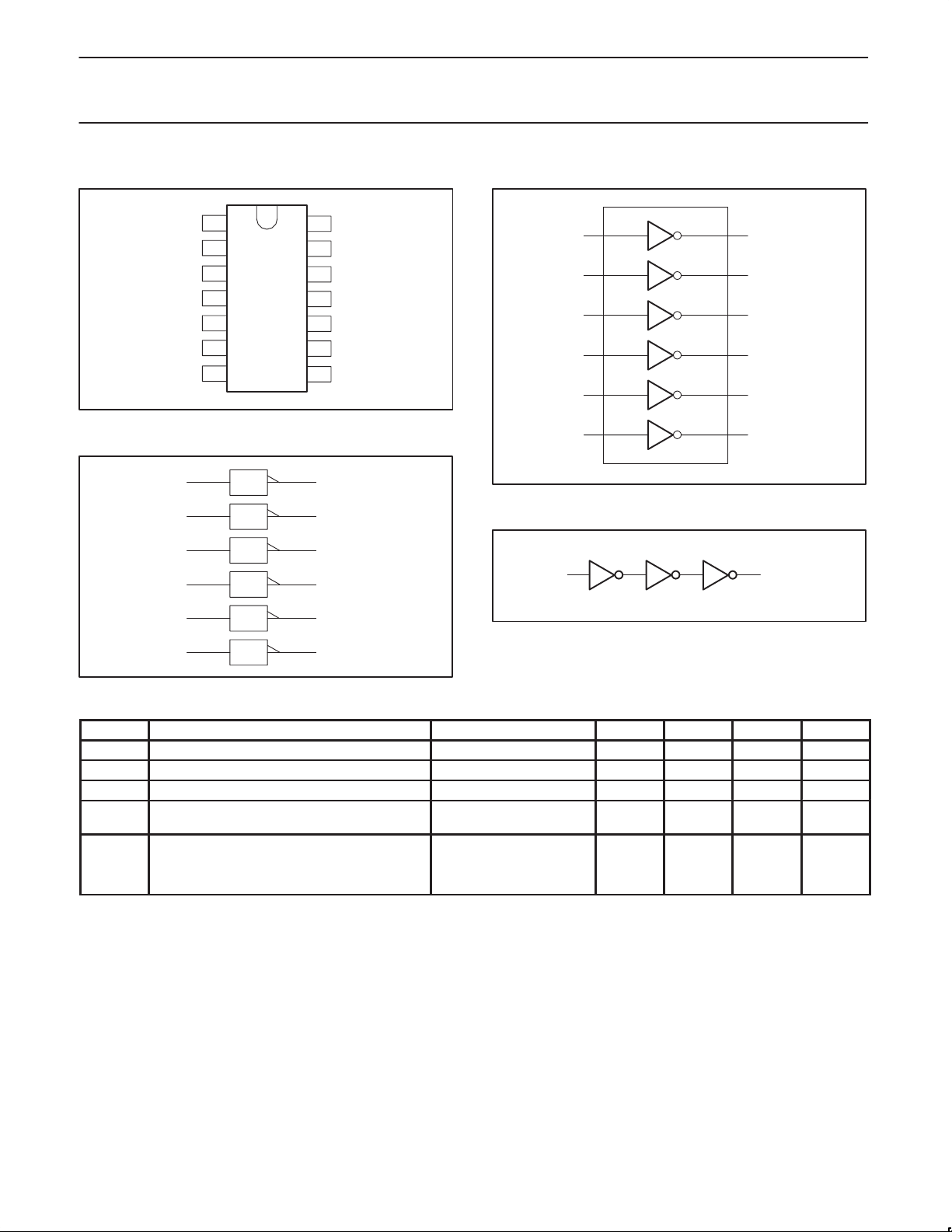
PIN DESCRIPTION
PIN NUMBER SYMBOL FUNCTION
1, 3, 5, 9, 11, 13 1A – 6A Data inputs
2, 4, 6, 8, 10, 12 1Y – 6Y Data outputs
7 GND Ground (0 V)
14 V
CC
Positive supply voltage
FUNCTION TABLE
INPUTS OUTPUTS
nA nY
L H
H L
NOTES:
H = HIGH voltage level
L =LOW voltage level
1998 Apr 20 853–1900 19257
2
Philips Semiconductors Product specification
Hex inverter
PIN CONFIGURATION
1
1A
2
1Y
3
2A
4
2Y
5
3A
6
3Y
GND
7
LOGIC SYMBOL (IEEE/IEC)
12
34
56
98
1
1
1
1
74LV04
LOGIC SYMBOL
14
V
CC
13
6A
12
6Y
11
5A
10
5Y
9
4A
8
4Y
SV00396
1A 1Y
1
2A
3
3A 3Y
5
9
4A 4Y
5A 5Y
11
6A
13
LOGIC DIAGRAM (ONE INVERTER)
AY
2
4
2Y
6
8
10
12
6Y
SV00397
11 10
13 12
1
1
SV00398
SV00399
RECOMMENDED OPERA TING CONDITIONS
SYMBOL PARAMETER CONDITIONS MIN TYP MAX UNIT
NO TAG
characteristics
= 2.0V to 2.7V
1.0 3.3 5.5 V
CC
CC
–40
–40
–
–
–
–
–
–
–
–
+85
+125
500
200
100
50
ns/V
T
V
V
V
amb
tr, t
DC supply voltage See Note
CC
Input voltage 0 – V
I
Output voltage 0 – V
O
Operating ambient temperature range in free air
Input rise and fall times
f
NOTE:
1. The LV is guaranteed to function down to V
See DC and AC
VCC = 1.0V to 2.0V
V
CC
VCC = 2.7V to 3.6V
VCC = 3.6V to 5.5V
= 1.0V (input levels GND or VCC); DC characteristics are guaranteed from VCC = 1.2V to VCC = 5.5V.
CC
V
V
°C
1998 Apr 20
3
 Loading...