

Philips 74HCT93U, 74HCT93N, 74HC93U, 74HC93DB, 74HC93D Datasheet
DATA SH EET
Product specification
File under Integrated Circuits, IC06
December 1990
INTEGRATED CIRCUITS
74HC/HCT93
4-bit binary ripple counter
For a complete data sheet, please also download:
•The IC06 74HC/HCT/HCU/HCMOS Logic Family Specifications
•The IC06 74HC/HCT/HCU/HCMOS Logic Package Information
•The IC06 74HC/HCT/HCU/HCMOS Logic Package Outlines

December 1990 2
Philips Semiconductors Product specification
4-bit binary ripple counter 74HC/HCT93
FEATURES
• Various counting modes
• Asynchronous master reset
• Output capability: standard
• ICC category: MSI
GENERAL DESCRIPTION
The 74HC/HCT93 are high-speed
Si-gate CMOS devices and are pin
compatible with low power Schottky
TTL (LSTTL). They are specified in
compliance with JEDEC standard
no. 7A.
The 74HC/HCT93 are 4-bit binary
ripple counters. The devices consist
of four master-slave flip-flops
internally connected to provide a
divide-by-two section and a
divide-by-eight section. Each section
has a separate clock input (
CP0 and
CP1) to initiate state changes of the
counter on the HIGH-to-LOW clock
transition. State changes of the Q
n
outputs do not occur simultaneously
because of internal ripple delays.
Therefore, decoded output signals
are subject to decoding spikes and
should not be used for clocks or
strobes.
A gated AND asynchronous master
reset (MR1 and MR2) is provided
which overrides both clocks and
resets (clears) all flip-flops.
Since the output from the
divide-by-two section is not internally
connected to the succeeding stages,
the device may be operated in various
counting modes. In a 4-bit ripple
counter the output Q0 must be
connected externally to input CP1.
The input count pulses are applied to
clock input CP0. Simultaneous
frequency divisions of 2, 4, 8 and 16
are performed at the Q0, Q1, Q2 and
Q3 outputs as shown in the function
table. As a 3-bit ripple counter the
input count pulses are applied to input
CP1.
Simultaneous frequency divisions of
2, 4 and 8 are available at the Q1, Q
2
and Q3 outputs. Independent use of
the first flip-flop is available if the reset
function coincides with reset of the
3-bit ripple-through counter.
QUICK REFERENCE DATA
GND = 0 V; T
amb
=25°C; tr=tf= 6 ns
Notes
1. C
PD
is used to determine the dynamic power dissipation (PD in µW):
PD=CPD× V
CC
2
× fi+∑(CL× V
CC
2
× fo) where:
fi= input frequency in MHz; fo= output frequency in MHz
∑ (CL× V
CC
2
× fo) = sum of outputs
CL= output load capacitance in pF; VCC= supply voltage in V
2. For HC the condition is VI= GND to VCC; for HCT the condition is VI= GND to VCC− 1.5 V
ORDERING INFORMATION
See
“74HC/HCT/HCU/HCMOS Logic Package Information”
.
SYMBOL PARAMETER CONDITIONS
TYPICAL
UNIT
HC HCT
t
PHL
/ t
PLH
propagation delay CP0 to Q
0
CL= 15 pF; VCC=5 V
12 15 ns
f
max
maximum clock frequency 100 77 MHz
C
I
input capacitance 3.5 3.5 pF
C
PD
power dissipation capacitance per package notes 1 and 2 22 22 pF
December 1990 3
Philips Semiconductors Product specification
4-bit binary ripple counter 74HC/HCT93
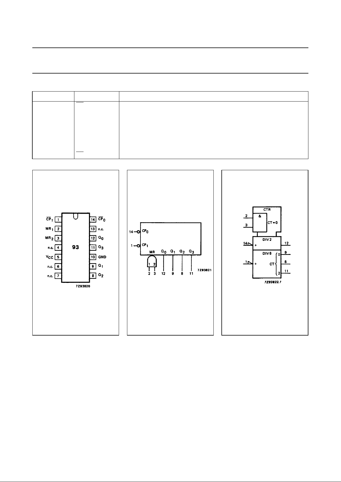
PIN DESCRIPTION
PIN NO. SYMBOL NAME AND FUNCTION
1
CP
1
clock input 2nd, 3rd and 4th section (HIGH-to-LOW, edge-triggered)
2, 3 MR
1
, MR
2
asynchronous master reset (active HIGH)
4, 6, 7, 13 n.c. not connected
5V
CC
positive supply voltage
10 GND ground (0 V)
12, 9, 8, 11 Q
0
to Q
3
flip-flop outputs
14
CP
0
clock input 1st section (HIGH-to-LOW, edge-triggered)
Fig.1 Pin configuration. Fig.2 Logic symbol. Fig.3 IEC logic symbol.
 Loading...