

Philips 74hct9046a DATASHEETS

INTEGRATED CIRCUITS
DATA SH EET
74HCT9046A
PLL with bandgap controlled VCO
Product specification
Supersedes data of March 1994
File under Integrated Circuits, IC06
1999 Jan 11
Philips Semiconductors Product specification
PLL with bandgap controlled VCO 74HCT9046A
FEATURES
• Low power consumption
• Centre frequency up to
17 MHz (typ.) at VCC = 5.5 V
• Choice of two phase
comparators
(1)
:
– EXCLUSIVE-OR (PC1)
– Edge-triggered JK flip-flop (PC2)
• No dead zone of PC2
• Charge pump output on PC2,
whose current is set by an external
resistor R
b
• Centre frequency tolerance ±10%
• Excellent
voltage-controlled-oscillator (VCO)
linearity
• Low frequency drift with supply
voltage and temperature variations
• On chip bandgap reference
• Glitch free operation of VCO, even
at very low frequencies
• Inhibit control for ON/OFF keying
and for low standby power
consumption
• Operation power supply voltage
range 4.5 to 5.5 V
• Zero voltage offset due to op-amp
buffering
• Output capability: standard
• ICC category: MSI.
APPLICATIONS
• Tone decoding
• Data synchronization and
conditioning
• Voltage-to-frequency conversion
• Motor-speed control.
GENERAL DESCRIPTION
The 74HCT9046A is a high-speed
Si-gate CMOS device. It is specified
in compliance with
no. 7A”
.
“JEDEC standard
QUICK REFERENCE DATA
GND = 0 V; T
= 25 °C; tr = tf≤ 6 ns.
amb
SYMBOL PARAMETER CONDITIONS TYP. UNIT
f
c
VCO centre frequency C1 = 40 pF;
16 MHz
R1 = 3 kΩ;
VCC= 5 V
C
I
C
PD
input capacitance 3.5 pF
power dissipation
notes 1 and 2 20 pF
capacitance per
package
Notes
1. C
is used to determine the dynamic power dissipation (PD in µW)
PD
a) PD = CPD× V
2
× fi + Σ(CL× V
CC
2
× fo) where:
CC
b) fi = input frequency in MHz; CL = output load capacity in pF;
fo = output frequency in MHz; VCC = supply voltage in V;
Σ(CL× V
2
× fo) = sum of the outputs.
CC
2. Applies to the phase comparator section only (inhibit = HIGH). For power
dissipation of the VCO and demodulator sections see Figs 26 to 28.
ORDERING INFORMATION
EXTENDED
TYPE NUMBER
PINS PIN POSITION MATERIAL CODE
PACKAGE
74HCT9046AN 16 DIL16 plastic SOT38Z
74HCT9046AD 16 SO16 plastic SOT109A
• FM modulation and demodulation
where a small centre frequency
tolerance is essential
• Frequency synthesis and
multiplication where a low jitter is
required (e.g. Video
picture-in-picture)
• Frequency discrimination
(1) Rb connected between pin 15 and
ground: PC2 mode, with PCP
pin 2.
Pin 15 left open or connected to V
PC1 mode with PC1
OUT
at pin 2.
OUT
at
CC
:
1999 Jan 11 2

Philips Semiconductors Product specification
PLL with bandgap controlled VCO 74HCT9046A
PINNING
SYMBOL PIN DESCRIPTION
GND 1 ground (0 V) (phase comparators)
PC1
PCP
COMP
VCO
INH 5 inhibit input
C1
C1
GND 8 ground (0 V) (VCO)
VCO
DEM
R1 11 resistor R1 connection
R2 12 resistor R2 connection
PC2
SIG
R
V
b
CC
A
B
OUT
OUT
OUT
IN
OUT
OUT
IN
/
2 phase comparator 1 output/phase
comparator pulse output
IN
3 comparator input
4 VCO output
6 capacitor C1 connection A
7 capacitor C1 connection B
9 VCO input
10 demodulator output
13 phase comparator 2 output
GND
PC1 /
OUT
PCP
OUT
COMP
VCO
OUT
C1
C1
GND
INH
1
2
3
IN
4
9046A
5
6
A
7
B
8
MBD037 - 1
V
16
CC
R
15
b
SIG
14
IN
PC2
13
OUT
R2
12
R1
11
DEM
10
9
VCO
OUT
IN
(current source adjustable with Rb)
14 signal input
15 bias resistor (Rb) connection
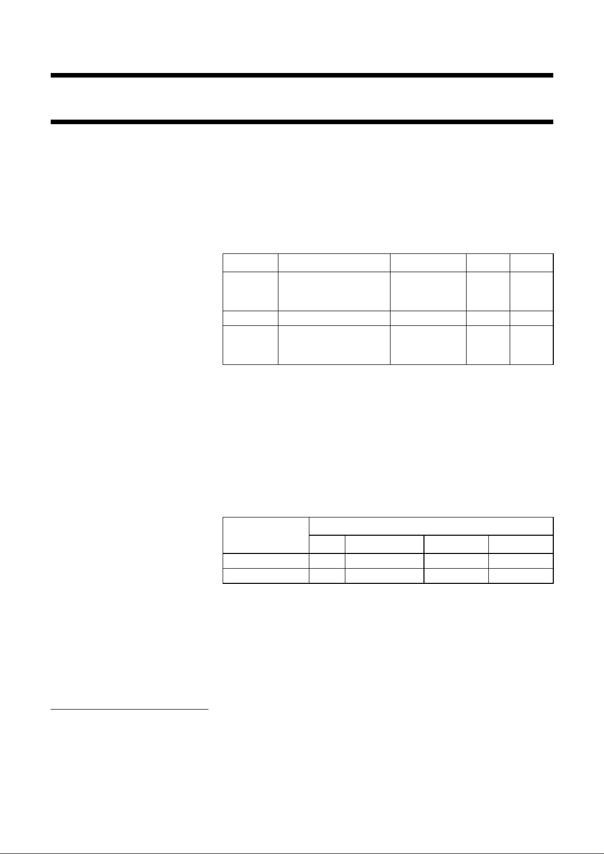
Fig.1 Pin configuration.
16 supply voltage
LOGIC/FUNCTIONAL SYMBOLS AND DIAGRAMS
PC1 /
14
15
11
12
COMP
3
6
7
9
5
SIG
R
b
C1
C1
R1
R2
VCO
INH
IN
Φ
IN
A
B
VCO
IN
PCP
PC2
VCO
DEM
MBD038 - 1
OUT
OUT
OUT
OUT
OUT
2
13
4
10
14
11
12
15
Φ
PLL
9046A
PC1 /
COMP
3
6
7
9
5
SIG
C1
C1
R1
R2
R
b
VCO
INH
IN
IN
A
B
IN
PCP
PC2
DEM
VCO
MBD039 - 1
OUT
OUT
OUT
OUT
OUT
2
13
10
4
Fig.2 Logic symbol.
1999 Jan 11 3
Fig.3 IEC logic symbol.
Philips Semiconductors Product specification
PLL with bandgap controlled VCO 74HCT9046A
C1
R2
R1
C1
A
12
R2
11
R1
5109
C1
VCO
DEM
R
B
s
VCO
OUT
COMP
314476
SIG
IN
IN
9046A
PC1 /
OUT
PHASE
COMPARATOR
1
PHASE
COMPARATOR
2
VCO
OUTINH
IN
PCP
OUT
2
PC2
13
OUT
R
15
b
R
b
R3
R4
C2
MBD040 - 1
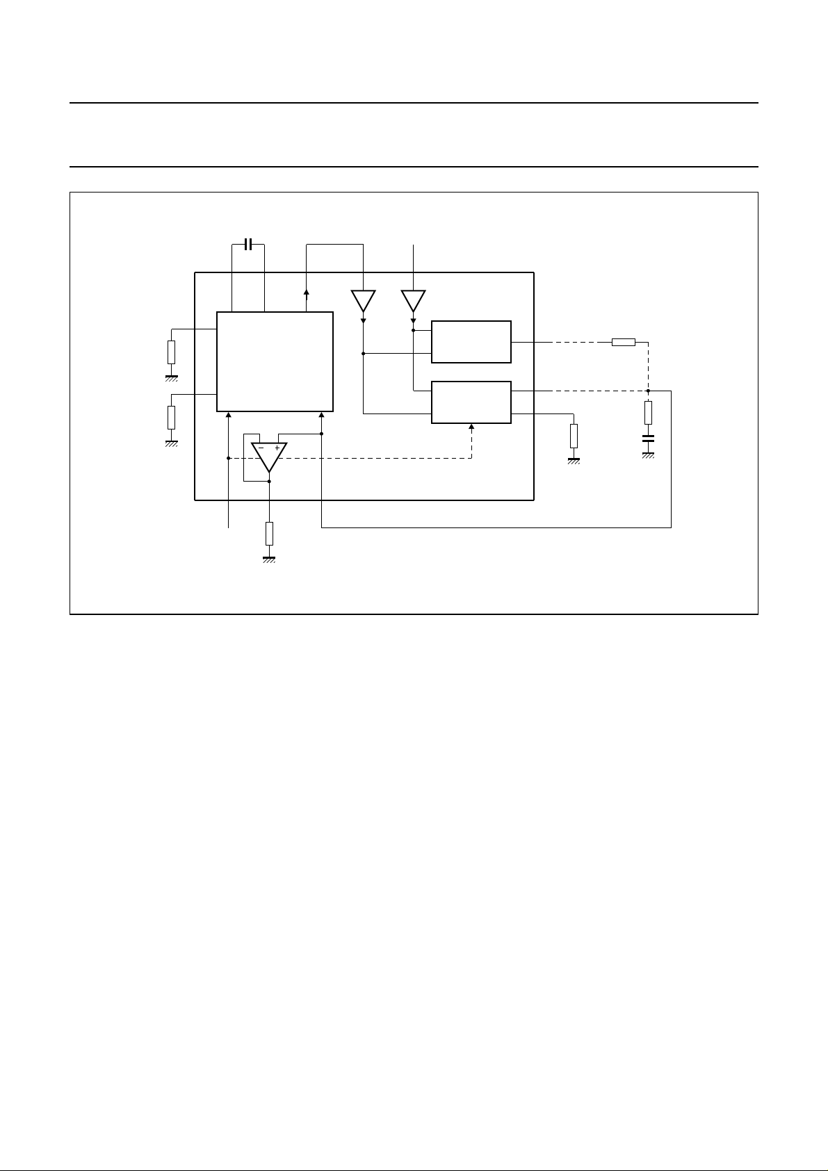
Fig.4 Functional diagram.
1999 Jan 11 4
This text is here in white to force landscape pages to be rotated correctly when browsing through the pdf in the Acrobat reader.This text is here in
_white to force landscape pages to be rotated correctly when browsing through the pdf in the Acrobat reader.This text is here inThis text is here in
white to force landscape pages to be rotated correctly when browsing through the pdf in the Acrobat reader. white to force landscape pages to be ...
1999 Jan 11 5
Philips Semiconductors Product specification
PLL with bandgap controlled VCO 74HCT9046A
R2
R1
R
f
VCO
OUT
OUT
V
ref1
BAND
GAP
COMP
V
ref2
C1
764
C1
C1
V
R2
12
R1
11
DEM
10
OUT
ref2
B
A
VCO
V
ref1
s
f
314
IN
IN
SIG
IN
PC1 /
OUT
PCP
OUT
PC2
OUT
R
2
R3
13
R4
C2
15
b
R
b
logic
1
logic
1
DQ
CP
Q
R
D
DQ
CP
Q
R
D
up
down
PC1
PCP
V
ref2
CHARGE
PUMP
9
VCO
5
IN
INH
MBD102 - 1
Fig.5 Logic diagram.

Philips Semiconductors Product specification
PLL with bandgap controlled VCO 74HCT9046A
FUNCTIONAL DESCRIPTION
The 74HCT9046A is a
phase-locked-loop circuit that
comprises a linear VCO and two
different phase comparators (PC1
and PC2) with a common signal input
amplifier and a common comparator
input (see Fig.4). The signal input can
be directly coupled to large voltage
signals (CMOS level), or indirectly
coupled (with a series capacitor) to
small voltage signals. A self-bias
input circuit keeps small voltage
signals within the linear region of the
input amplifiers. With a passive
low-pass filter, the '9046A' forms a
second-order loop PLL.
The principle of this
phase-locked-loop is based on the
familiar HCT4046A. However extra
features are built in, allowing very
high performance phase-locked-loop
applications. This is done, at the
expense of PC3, which is skipped in
this HCT9046A. The PC2 is equipped
with a current source output stage
here. Further a bandgap is applied for
all internal references, allowing a
small centre frequency tolerance. The
details are summed up in the next
section called: “Differences with
respect to the familiar HCT4046A”.
If one is familiar with the HCT4046A
already, it will do to read this section
only.
DIFFERENCES WITH RESPECT TO THE FAMILIAR HCT4046A
• A centre frequency tolerance of
maximum ±10%.
• The on board bandgap sets the
internal references resulting in a
minimal frequency shift at supply
voltage variations and temperature
variations.
• The value of the frequency offset is
determined by an internal
reference voltage of 2.5 V instead
− 0.7 V. In this way the offset
of V
CC
frequency will not shift over the
supply voltage range.
• A current switch charge pump
output on PC2 allows a virtually
ideal performance of PC2. The gain
of PC2 is independent of the
voltage across the low-pass filter.
Further a passive low-pass filter in
the loop achieves an active
performance now. The influence of
the parasitic capacitance of the
PC2 output plays no role here,
resulting in a true correspondence
of the output correction pulse and
the phase difference even up to
phase differences as small as a few
nanoseconds.
• Because of its linear performance
without dead zone, higher
impedance values for the filter,
hence lower C-values, can now be
chosen. Correct operation will not
be influenced by parasitic
capacitances as in the instance
with voltage source output of the
4046A.
• No PC3 on pin 15 but instead a
resistor connected to GND, which
sets the load/unload currents of the
charge pump (PC2).
• Extra GND pin at pin 1 to allow an
excellent FM demodulator
performance even at 10 MHz and
higher.
• Combined function of pin 2. If
pin 15 is connected to V
(no bias
CC
resistor Rb) pin 2 has its familiar
function viz. output of PC1. If at
pin 15 a resistor (Rb) is connected
to GND it is assumed that PC2 has
been chosen as phase comparator.
Connection of Rb is sensed by
internal circuitry and this changes
the function of pin 2 into a lock
detect output (PCP
same characteristics as PCP
) with the
OUT
OUT
of
pin 1 of the well known
74HCT4046A.
• The inhibit function differs. For the
HCT4046A a HIGH level at the
inhibit input (INH) disables the VCO
and demodulator, while a LOW
level turns both on. For the
74HCT9046A a HIGH level on the
inhibit input disables the whole
circuit to minimize standby power
consumption.
VCO
The VCO requires one external
capacitor C1 (between C1
and C1B)
A
and one external resistor R1
(between R1 and GND) or two
external resistors R1 and R2
(between R1 and GND, and R2 and
GND). Resistor R1 and capacitor C1
determine the frequency range of the
VCO. Resistor R2 enables the VCO
to have a frequency offset if required
(see Fig.5).
The high input impedance of the VCO
simplifies the design of the low-pass
filters by giving the designer a wide
choice of resistor/capacitor ranges. In
order not to load the low-pass filter, a
demodulator output of the VCO input
voltage is provided at pin 10
(DEM
). The DEM
OUT
OUT
voltage
equals that of the VCO input. If
DEM
is used, a load resistor (Rs)
OUT
should be connected from pin 10 to
GND; if unused, DEM
left open. The VCO output (VCO
should be
OUT
OUT
can be connected directly to the
comparator input (COMPIN), or
connected via a frequency-divider.
The VCO output signal has a duty
factor of 50% (maximum expected
deviation 1%), if the VCO input is held
at a constant DC level. A LOW level at
the inhibit input (INH) enables the
VCO and demodulator, while a HIGH
level turns both off to minimize
standby power consumption.
)
1999 Jan 11 6

Philips Semiconductors Product specification
PLL with bandgap controlled VCO 74HCT9046A
Phase comparators
The signal input (SIGIN) can be
directly coupled to the self-biasing
amplifier at pin 14, provided that the
signal swing is between the standard
HC family input logic levels.
Capacitive coupling is required for
signals with smaller swings.
P
HASE COMPARATOR 1 (PC1)
This circuit is an EXCLUSIVE-OR
network. The signal and comparator
input frequencies (f
) must have a
i
50% duty factor to obtain the
maximum locking range. The transfer
characteristic of PC1, assuming
ripple (f
V
= 2fi) is suppressed, is:
r
V
CC
DEMOUT
---------- -
π
–()=
Φ
SIGINΦCOMPIN
where:
V
DEMOUT
is the demodulator output
at pin 10.
V
DEMOUT
= V
PC1OUT
(via low-pass).
The phase comparator gain is:
V
K
CC
Vr⁄()=
---------- -
p
π
The average output voltage from
PC1, fed to the VCO input via the
low-pass filter and seen at the
demodulator output at pin 10
(V
DEMOUT
), is the resultant of the
phase differences of signals (SIGIN)
and the comparator input (COMPIN)
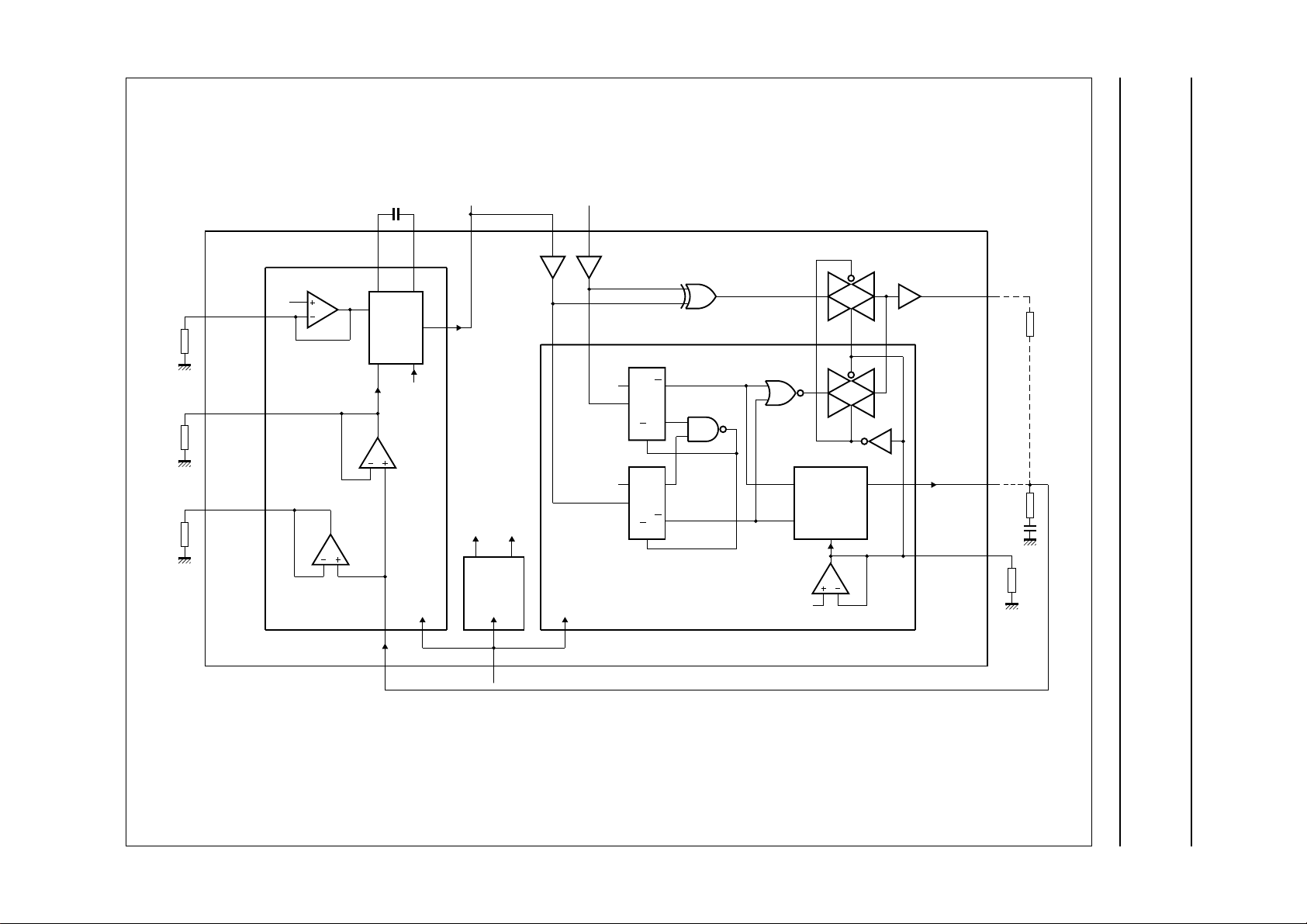
as shown in Fig.6. The average of
V
DEMOUT
there is no signal or noise at SIG
is equal to1⁄2VCC when
IN
and with this input the VCO oscillates
at the centre frequency (fc). Typical
waveforms for the PC1 loop locked at
fc are shown in Fig.7. This figure also
shows the actual waveforms across
the VCO capacitor at pins 6 and 7
(V
C1A
and V
) to show the relation
C1B
between these ramps and the
VCO
OUT
voltage.
The frequency capture range (2f
c
) is
defined as the frequency range of
input signals on which the PLL will
lock if it was initially out-of-lock. The
frequency lock range (2fL) is defined
as the frequency range of the input
signals on which the loop will stay
locked if it was initially in lock. The
capture range is smaller or equal to
the lock range.
With PC1, the capture range depends
on the low-pass filter characteristics
and can be made as large as the lock
range. This configuration remains
locked even with very noisy input
signals. Typical behaviour of this type
of phase comparator is that it may
lock to input frequencies close to the
harmonics of the VCO centre
frequency.
P
HASE COMPARATOR 2 (PC2)
This is a positive edge-triggered
phase and frequency detector. When
the PLL is using this comparator, the
loop is controlled by positive signal
transitions and the duty factors of
SIGIN and COMPIN are not important.
PC2 comprises two D-type flip-flops,
control gating and a 3-state output
stage with sink and source transistors
acting as current sources, henceforth
called charge pump output of PC2.
The circuit functions as an up-down
counter (Fig.5) where SIGIN causes
an up-count and COMPIN a down
count. The current switch charge
pump output allows a virtually ideal
performance of PC2, due to appliance
of some pulse overlap of the up and
down signals. See Fig.8a.
1999 Jan 11 7

Philips Semiconductors Product specification
PLL with bandgap controlled VCO 74HCT9046A
V
DEMOUTVPC1OUT
Φ
PCIN
Φ
SIGINΦCOMPIN
Fig.6 Phase comparator 1; average output voltage as a function of input phase difference.
–()=
V
---------- -
CC
Φ
π
V
DEMOUT(AV)
–()==
SIGINΦCOMPIN
1/2V
Φ
MBD101 - 1
PCIN
180
o
V
CC
CC
0
o
0
o
90
SIGN
IN
COMP
IN
VCO
OUT
PC1
OUT
VCO
IN
V
C1A
V
C1B
Fig.7 Typical waveforms for PLL using phase comparator 1; loop-locked at fc.
1999 Jan 11 8
V
CC
GND
pin 6
pin 7
MBD100

Philips Semiconductors Product specification
PLL with bandgap controlled VCO 74HCT9046A
The pump current IP is independent
from the supply voltage and is set by
the internal bandgap reference of
2.5 V.
17
2.5
-------R
A()×=
b
I
P
is the external bias resistor
R
b
between pin 15 and ground.
The current and voltage transfer
function of PC2 are shown in Fig.9.
The phase comparator gain is:
I
P
------2π
Ar⁄()=
K
p
Typical waveforms for the PC2 loop
locked at f
are shown in Fig.10.
c
When the frequencies of SIGIN and
COMPIN are equal but the phase of
SIGIN leads that of COMPIN, the up
output driver at PC2
is held ‘ON’
OUT
for a time corresponding to the phase
difference (Φ
). When the phase of
PCIN
SIGIN lags that of COMPIN, the down
or sink driver is held ‘ON’.
When the frequency of SIGIN is higher
than that of COMPIN, the source
output driver is held ‘ON’ for most of
the input signal cycle time and for the
remainder of the cycle time both
drivers are ‘OFF’ (3-state). If the
SIGIN frequency is lower than the
COMPIN frequency, then it is the sink
driver that is held ‘ON’ for most of the
cycle. Subsequently the voltage at the
capacitor (C2) of the low-pass filter
connected to PC2
varies until the
OUT
signal and comparator inputs are
equal in both phase and frequency. At
this stable point the voltage on C2
remains constant as the PC2 output is
in 3-state and the VCO input at pin 9
is a high impedance. Also in this
condition the signal at the phase
comparator pulse output (PCP
OUT
)
has a minimum output pulse width
equal to the overlap time, so can be
used for indicating a locked condition.
Thus for PC2 no phase difference
exists between SIGIN and COMP
IN
over the full frequency range of the
VCO. Moreover, the power
dissipation due to the low-pass filter is
reduced because both output drivers
are OFF for most of the signal input
cycle. It should be noted that the PLL
lock range for this type of phase
comparator is equal to the capture
range and is independent of the
low-pass filter. With no signal present
at SIGIN the VCO adjust, via PC2, to
its lowest frequency.
By using current sources as charge
pump output on PC2, the dead zone
or backlash time could be reduced to
zero. Also, the pulse widening due to
the parasitic output capacitance plays
no role here. This enables a linear
transfer function, even in the vicinity
of the zero crossing. The differences
between a voltage switch charge
pump and a current switch charge
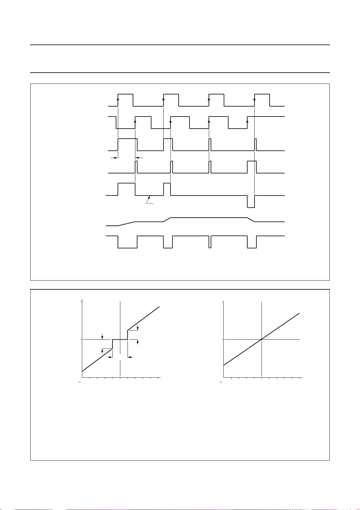
pump are shown in Fig.11.
The design of the low-pass filter is
somewhat different when using
current sources. The external resistor
R3 is no longer present when using
PC2 as phase comparator. The
current source is set by Rb. A simple
capacitor behaves as an ideal
integrator now, because the capacitor
is charged by a constant current. The
transfer function of the voltage switch
charge pump may be used. In fact it is
even more valid, because the transfer
function is no longer restricted for
small changes only. Further the
current is independent from both the
supply voltage and the voltage across
the filter. For one that is familiar with
the low-pass filter design of the
4046A a relation may show how R
b
relates with a fictive series resistance,
called R3'.
This relation can be derived by
assuming first that a voltage
controlled switch PC2 of the 4046A is
connected to the filter capacitance C2
via this fictive R3' (see Fig.8b). Then
during the PC2 output pulse the
charge current equals:
V
–
=
-----------------------------------
P
CCVC2 0()
R3'
I
P
at:
C2(0)
2.5
=
-------- R3'
I
With the initial voltage V
1
⁄2VCC = 2.5 V,
As shown before the charge current
of the current switch of the 9046A is:
2.5
17
×=
------- R
b
I
P
Hence:
R
------ 17
b
Ω()=
R3'
Using this equivalent resistance R3'
for the filter design the voltage can
now be expressed as a transfer
function of PC2; assuming ripple
(f
) is suppressed, as:
r=fi
5
K
PC2
------ 4π
Vr⁄()=
Again this illustrates the supply
voltage independent behaviour of
PC2.
Examples of PC2 combined with a
passive filter are shown in Figs 12
and 13. Figure 12 shows that PC2
with only a C2 filter behaves as a
high-gain filter. For stability the
damped version of Fig.13 with series
resistance R4 is preferred.
Practical design values for R
are
b
between 25 and 250 kΩ with
R3' = 1.5 to 15 kΩ for the filter design.
Higher values for R3' require lower
values for the filter capacitance which
is very advantageous at low values
the loop natural frequency ω
.
n
1999 Jan 11 9

Philips Semiconductors Product specification
PLL with bandgap controlled VCO 74HCT9046A
V
CC
up
V
CC
I
P
PC2
∆ Φ = Φ
PCIN
pulse overlap of
approximately 15 ns
down
OUT
I
P
C2
MBD046 - 1
up
R3'
I
down C2
P
PC2
VC2
OUT
OUT
MBD099
a. At every ∆Φ, even at zero∆Φ both switches are closed simultaneously for a short period (typically 15 ns).
b. Comparable voltage-controlled switch.
Fig.8 The current switch charge pump output of PC2.
Φ
MSB306 - 1
PCIN
I
P
0
I
P
20
π
Φ
PCIN
2
π
V
DEMOUT(AV)
1/2V
V
CC
CC
0
20
π
b.a.
b.a.
I x R
P
PCIN
Φ
=
SIGINΦCOMPIN
Φ
2
π
Two kinds of transfer functions may be regarded:
I
Φ
PCIN
------2π
P
Φ
PCIN
by connecting a resistor (R = 10 kΩ) between PC2
OUT
a. The current transfer:
b. The voltage transfer; this transfer can be observed at PC2
V
==
DEMOUTVPC2OUT
pump current
5
------ 4π
Fig.9 Phase comparator 2.
1999 Jan 11 10
and1⁄2VCC;
OUT
Philips Semiconductors Product specification
PLL with bandgap controlled VCO 74HCT9046A
SIG
IN
COMP
IN
VCO
OUT
UP
OPC
IN
DOWN
CURRENT AT
PC2
OUT
high impedance OFF state,
(zero current)
PC2 /VCO
OUT IN
PCP
OUT
The pulse overlap of the up and down signals (typically 15 ns).
Fig.10 Timing diagram for PC2.
2.75
VCO
IN
2.50
2.25
(1)
25
(1)
(2)
025
phase error (ns)
VCO
2.75
IN
2.50
2.25
MBD047 - 1
25
025
phase error (ns)
a. Response with traditional voltage-switch charge-pump PC2
(1) Due to parasitic capacitance on PC2
(2) Backlash time (dead zone).
b. Response with current switch charge-pump PC2
OUT
.
as applied in the HCT9046A.
OUT
OUT
(4046A).
Fig.11 The response of a locked-loop in the vicinity of the zero crossing of the phase error.
1999 Jan 11 11
b.a.
MBD043
Philips Semiconductors Product specification
PLL with bandgap controlled VCO 74HCT9046A
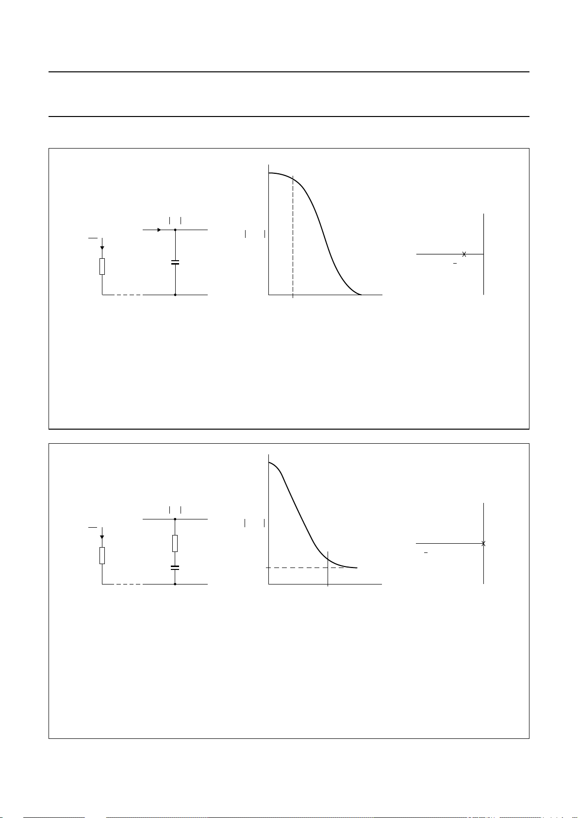
LOOP FILTER COMPONENT SELECTION
A
I
P
I
P
17
R
b
C2
F
ωj()
1/OUTPUTINPUT
τ
A
1
R
b
a.
τ
1
b. Amplitude characteristic:
c. Pole zero diagram.
C2× R3' C2×==
------ 17
I
P
17
R
b
1/
τ
A
1
ω
a. b. c.
F
---------------------------- -
jω()
1A⁄ jωτ1+
1
1
≈=
----------j ωτ
1
Fig.12 Simple loop filter for PC2 without damping.
A
I
P
F
ωj()
R4
C2
OUTPUTINPUT
m
MBD045 - 1
O
1/
τ
2
1/
τ
A
1
1/
τ
A
1
a. b. c.
R
b
a.
τ
1
τ
2
b. Amplitude characteristic:
c. Pole zero diagram.
A = DC gain limit, due to leakage.
C2× R3' C2×==
------ 17
R4 C2×=
jω()
1jωτ2+
=
---------------------------- 1A⁄ jωτ
+
1
F
Fig.13 Simple loop filter for PC2 with damping.
1999 Jan 11 12
1 /
ω
τ
2
MBD044 - 1
 Loading...