

Philips 74HCT75N, 74HCT75DB, 74HCT75D, 74HC75U, 74HC75PW Datasheet
...
DATA SH EET
Product specification
File under Integrated Circuits, IC06
December 1990
INTEGRATED CIRCUITS
74HC/HCT75
Quad bistable transparent latch
For a complete data sheet, please also download:
•The IC06 74HC/HCT/HCU/HCMOS Logic Family Specifications
•The IC06 74HC/HCT/HCU/HCMOS Logic Package Information
•The IC06 74HC/HCT/HCU/HCMOS Logic Package Outlines
December 1990 2
Philips Semiconductors Product specification
Quad bistable transparent latch 74HC/HCT75
FEATURES
• Complementary Q and Q outputs
• VCC and GND on the centre pins
• Output capability: standard
• ICC category: MSI
GENERAL DESCRIPTION
The 74HC/HCT75 are high-speed Si-gate CMOS devices
and are pin compatible with low power Schottky TTL
(LSTTL). They are specified in compliance with JEDEC
standard no. 7A.
The 74HC/HCT75 have four bistable latches. The two
latches are simultaneously controlled by one of two active
HIGH enable inputs (LE
1-2
and LE
3-4
). When LE
n-n
is
HIGH, the data enters the latches and appears at the nQ
outputs. The nQ outputs follow the data inputs (nD) as long
as LE
n-n
is HIGH (transparent). The data on the nD inputs
one set-up time prior to the HIGH-to-LOW transition of the
LE
n-n
will be stored in the latches. The latched outputs
remain stable as long as the LE
n-n
is LOW.
QUICK REFERENCE DATA
GND = 0 V; T
amb
=25°C; tr=tf=6ns
Notes
1. C
PD
is used to determine the dynamic power dissipation (PD in µW):
PD=CPD× V
CC
2
× fi+∑ (CL× V
CC
2
× fo) where:
fi= input frequency in MHz
fo= output frequency in MHz
∑ (CL× V
CC
2
× fo) = sum of outputs
CL= output load capacitance in pF
VCC= supply voltage in V
2. For HC the condition is VI= GND to V
CC
For HCT the condition is VI= GND to VCC−1.5 V
ORDERING INFORMATION
See
“74HC/HCT/HCU/HCMOS Logic Package Information”
.
SYMBOL PARAMETER CONDITIONS
TYPICAL
UNIT
HC HCT
t
PHL
/ t
PLH
propagation delay CL= 15 pF; VCC=5V
nD to nQ, n
Q1112ns
LE
n-n
to nQ, nQ1111ns
C
I
input capacitance 3.5 3.5 pF
C
PD
power dissipation capacitance per latch notes 1 and 2 42 42 pF
December 1990 3
Philips Semiconductors Product specification
Quad bistable transparent latch 74HC/HCT75
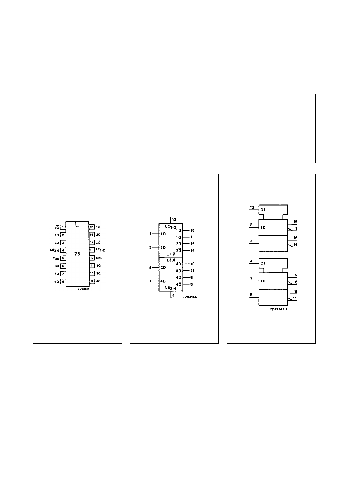
PIN DESCRIPTION
PIN NO. SYMBOL NAME AND FUNCTION
1, 14, 11, 8 1
Q to 4Q complementary latch outputs
2, 3, 6, 7 1D to 4D data inputs
4LE
3-4
latch enable input, latches 3 and 4 (active HIGH)
5V
CC
positive supply voltage
12 GND ground (0 V)
13 LE
1-2
latch enable input, latches 1 and 2 (active HIGH)
16, 15, 10, 9 1Q to 4Q latch outputs
Fig.1 Pin configuration. Fig.2 Logic symbol. Fig.3 IEC logic symbol.
 Loading...