

Philips 74HCT7403N, 74HCT7403D, 74HC7403N, 74HC7403D Datasheet
INTEGRATED CIRCUITS
DATA SH EET
For a complete data sheet, please also download:
•The IC06 74HC/HCT/HCU/HCMOS Logic Family Specifications
•The IC06 74HC/HCT/HCU/HCMOS Logic Package Information
•The IC06 74HC/HCT/HCU/HCMOS Logic Package Outlines
74HC/HCT7403
4-Bit x 64-word FIFO register;
3-state
Product specification
Supersedes data of October 1990
File under Integrated Circuits, IC06
September 1993
Philips Semiconductors Product specification
4-Bit x 64-word FIFO register; 3-state 74HC/HCT7403
FEATURES
• Synchronous or asynchronous
operation
• 3-state outputs
• 30 MHz (typical) shift-in and
shift-out rates
• Readily expandable in word and bit
dimensions
• Pinning arranged for easy board
layout: input pins directly opposite
output pins
• Output capability: driver (8 mA)
• ICC category: LSI.
APPLICATIONS
• High-speed disc or tape controller
• Communications buffer.
GENERAL DESCRIPTION
The 74HC/HCT7403 are high-speed
Si-gate CMOS devices. They are
specified in compliance with JEDEC
standard no.7A.
QUICK REFERENCE DATA
GND = 0 V; T
= 25 °C; tr = tf = 6 ns.
amb
TYP.
SYMBOL PARAMETER CONDITIONS
HC HCT
t
PHL/tPLH
f
max
propagation delay SO,
SI to DIR and DOR
maximum clock
CL = 15 pF;
VCC = 5 V
15 17 ns
30 30 MHz
frequency
C
I
C
PD
input capacitance 3.5 3.5 pF
power dissipation
note 1 475 490 pF
capacitance per
package
Note
1. For HC the condition is V
= GND to VCC.
I
For HCT the condition is VI = GND to VCC−1.5 V.
ORDERING INFORMATION
EXTENDED
TYPE NUMBER
PINS PIN POSITION MATERIAL CODE
PACKAGE
74HC/HCT7403N 16 DIL plastic SOT38Z
74HC/HCT7403D 16 SO16L plastic SOT162
UNIT
The “7403” is an expandable, First-In
First-Out (FIFO) memory organized
as 64 words by 4 bits. A guaranteed
15 MHz data-rate makes it ideal for
high-speed applications. A higher
data-rate can be obtained in
applications where the status flags
are not used (burst-mode).
With separate controls for shift-in (SI)
and shift-out (
SO), reading and
writing operations are completely
independent, allowing synchronous
and asynchronous data transfers.
Additional controls include a
master-reset input (MR), an output
enable input (OE) and flags. The
data-in-ready (DIR) and
data-out-ready (DOR) flags indicate
the status of the device.
September 1993 2
Philips Semiconductors Product specification
4-Bit x 64-word FIFO register; 3-state 74HC/HCT7403
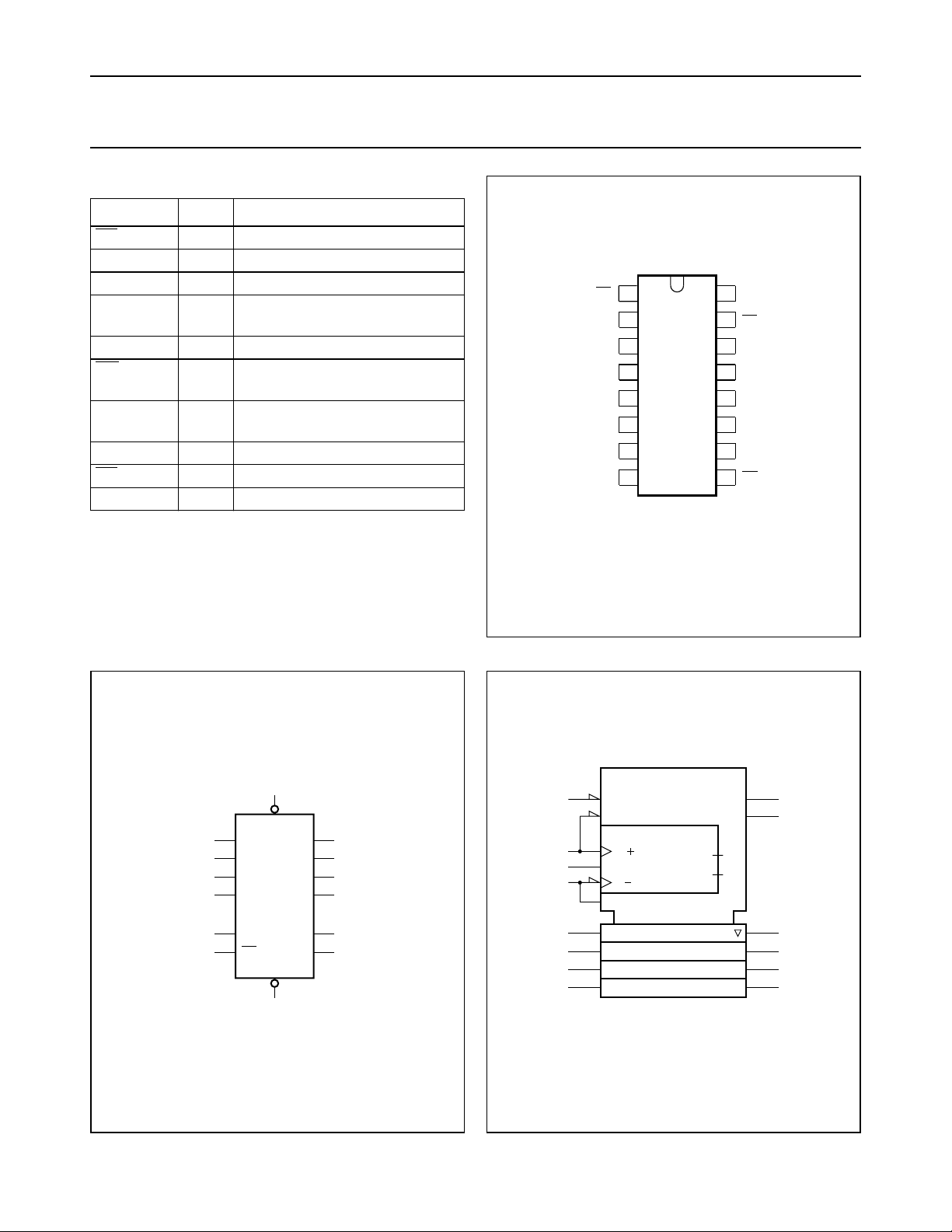
PINNING
SYMBOL PIN DESCRIPTION
OE 1 output enable input (active LOW)
DIR 2 data-in-ready output
SI 3 shift-in input (active HIGH)
D
to D
O
4, 5,
3
parallel data input
6, 7
GND 8 ground
MR 9 asynchronous master-reset
input (active LOW)
Q
to Q
3
10, 1 1,
0
data output
12, 13
DOR 14 data-out-ready output
SO 15 shift-out input (active LOW)
V
CC
16 positive supply voltage
handbook, halfpage
OE
DIR
D
D
D
D
GND
1
2
SI
3
4
0
1
2
3
7403
5
6
7
8
MGA672
V
16
CC
15
SO
14
DOR
Q
13
0
Q
12
1
Q
11
2
Q
10
3
9
MR
handbook, halfpage
Fig.1 Pin configuration.
1
OE
D
4
D
5
D
6
D
7
SI
3
15
SO
Q
13
MR
9
Q
Q
Q
DOR
DIR
0
1
2
3
MGA674
12
11
10
14
2
0
1
2
3
handbook, halfpage
1
3
9
15
4
5
6
7
EN4
1Z2
1 ( /C2)
CT = 0
5
5Z6
2D
FIFO 64 x 4
CTR
<
CT 64
CT 0
>
[IR] 3
[OR] 6
G1
G5
MGA676
2
14
13
4
12
11
10
Fig.2 Logic symbol.
September 1993 3
Fig.3 IEC logic symbol.
Philips Semiconductors Product specification
4-Bit x 64-word FIFO register; 3-state 74HC/HCT7403
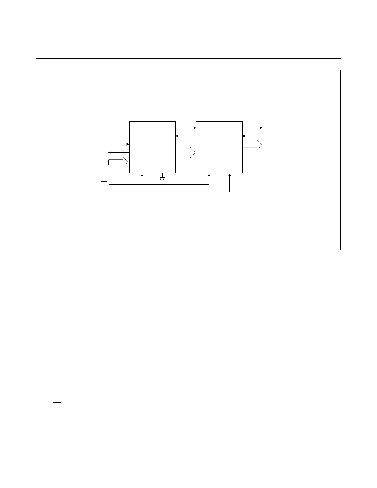
SI
DIR
DATA INPUT
4
MR
OE
FUNCTIONAL DESCRIPTION
A DIR flag indicates the input stage
status, either empty and ready to
receive data (DIR = HIGH) or full and
busy (DIR = LOW). When DIR and SI
are HIGH, data present at D0 to D3 is
shifted into the input stage; once
complete DIR goes LOW. When SI is
set LOW, data is automatically shifted
to the output stage or to the last
empty location. A FIFO which can
receive data is indicated by DIR set
HIGH.
SI
B
DIR
B
4
D
nB
MR
SI
DIR
D
nA
A
A
MR
7403
FIFO A
DOR
OE
SO
Q
A
A
nA
Fig.4 Functional diagram.
Expanded format (see Fig.17)
The DOR and DIR signals are used to
allow the “7403” to be cascaded. Both
parallel and serial expansion is
possible.
Serial expansion is only possible with
typical devices.
Parallel expansion
Parallel expansion is accomplished
by logically ANDing the DOR and DIR
signals to form a composite signal.
7403
FIFO B
DOR
OE
4
DOR
SO
DATA OUTPUT
SO
Q
B
B
nB
MGA679
Serial expansion
Serial expansion is accomplished by:
• tying the data outputs of the first
device to the data inputs of the
second device
• connecting the DOR pin of the first
device to the SI pin of the second
device
• connecting the SO pin of the first
device to the DIR pin of the second
device.
A DOR flag indicates the output stage
status, either data available (DOR =
HIGH) or busy (DOR = LOW). When
SO and DOR are HIGH, data is
available at the outputs (Q0 to Q3).
When SO is set LOW new data may
be shifted into the output stage, once
complete DOR is set HIGH.
September 1993 4
Philips Semiconductors Product specification
4-Bit x 64-word FIFO register; 3-state 74HC/HCT7403
DOR
ll pagewidth
SO
FP
(1)
R
SQ
R
61 x
FB
(1)
R
(2)
FF64
R
RQ
to
FF3
FF63
R
RQ
SQ
SQ
SQ
OE
Q0Q
CL CL
CL CL
1
3-STATE
4
4
OUTPUT
LATCHES
LATCHES
Q2Q
BUFFER
3
MSB118
position 64
position 3 to 63
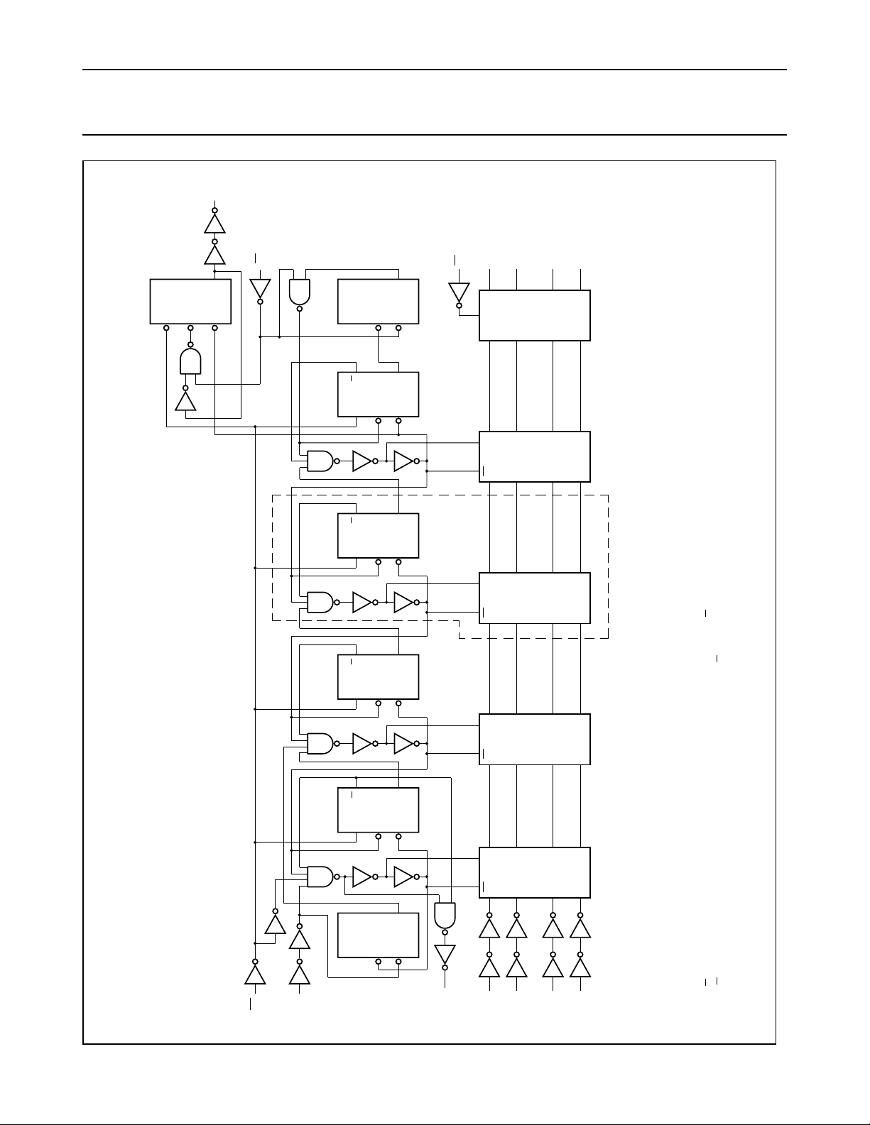
Fig.5 Logic diagram.
(2)
FF2
RQ
SQ
R
(2)
FF1
SQ
R
FS
SQ
R
MR
RQ
(1)
SI
September 1993 5
DIR
4
CL CL
CL CL
D0D1D2D
LATCHES
4
LATCHES
3
position 2
position 1
R input of FF1 to FF64 will set Q output to LOW independent of state on S input.
S input of flip-flops FS, FB and FP will set Q output to HIGH independent of state on R input.
LOW on
(see control flip-flops)
LOW on
Philips Semiconductors Product specification
4-Bit x 64-word FIFO register; 3-state 74HC/HCT7403
DC CHARACTERISTICS FOR 74HC
For the DC characteristics see
“74HC/HCT/HCU/HCMOS Logic Family Specifications”
valid for driver output.
They are replaced by the values given below.
Output capability: driver 8 mA
ICC category: LSI.
Voltages are referenced to GND (ground = 0 V).
DC CHARACTERISTICS FOR 74HC
SYMBOL PARAMETER
+25 −40 to +85 −40 to +125
MIN TYP MAX MIN MAX MIN MAX
V
OH
V
OH
HIGH level
output voltage
all outputs
HIGH level
output voltage
1.9
4.4
5.9
3.98
5.48
2.0
4.5
6
4.32
5.81−−
driver outputs
V
OL
V
OL
LOW level
output voltage
all outputs
LOW level
output voltage
−
−
−
−
−
0
0
0
0.15
0.15
driver outputs
T
−
−
−
0.1
0.1
0.1
0.26
0.26−−
(°C)
amb
1.9
4.4
5.9
3.84
5.34−−
−
−
−
−
−
−
0.1
0.1
0.1
0.33
0.33−−
1.9
4.4
5.9
3.70
5.20−−
−
−
−
−
−
−
0.1
0.1
0.1
0.40
0.40VV
, except that VOH and VOL are not
TEST CONDITION
UNIT
V
V
V
V
V
V
V
V
V
(V)
2.0
4.5
6.0
4.5
6.0
2.0
4.5
6.0
4.5
6.0
CC
V
or
V
V
or
V
V
or
V
V
or
V
V
I
IH
IL
IH
IL
IH
IL
IH
IL
OTHER
IO = −20 µA
IO = −8 mA
IO = −10 mA
IO = 20 µA
IO = 8 mA
IO = 10 mA
September 1993 6
Philips Semiconductors Product specification
4-Bit x 64-word FIFO register; 3-state 74HC/HCT7403
AC CHARACTERISTICS FOR 74HC
GND = 0 V; t
= tf = 6 ns; CL = 50 pF.
r
SYMBOL PARAMETER
t
PHL/tPLH
propagation
delay
MR to DIR,
DOR
t
PHL
propagation
delay
t
PHL/tPLH
MR to Q
propagation
n
delay
SI to DIR
t
PHL/tPLH
propagation
delay
SO to DOR
t
PHL/tPLH
propagation
delay
t
PHL/tPLH
DOR to Q
propagation
n
delay
t
PLH
SO to Q
propagation
n
delay/ripple
through delay
SI to DOR
t
PLH
propagation
delay/bubble-up
delay
SO to DIR
t
PZH/tPZL
3-state output
enable
t
PHZ/tPLZ
OE to Q
3-state output
n
disable
t
THL/tTLH
OE to Q
output
n
transition time−−
t
W
SI pulse
width
HIGH or LOW
t
W
SO pulse
width
HIGH or LOW
(°C)
T
amb
+25 −40 to +85 −40 to +125
MIN TYP MAX MIN MAX MIN MAX
−
−
−
−
−
−
−
−
−
−
−
−
−
−
−
−
−
−
−
−
−
−
−
−
−
−
−
−
−
−
−
35
7
6.0
70
14
12
69
25
20
52
19
15
66
24
19
94
34
27
11
4
3
105
38
30
2.2
0.8
0.6
2.8
1.0
0.8
44
16
13
50
18
14
14
5
4
11
4
3
22
8
6.0
210
42
36
160
32
27
205
41
35
290
58
49
35
7
6.0
325
65
55
7
1.4
1.2
9
1.8
1.5
150
30
26
150
30
26
60
12
10
−
−
−
−
−
−
−
−
−
−
−
−
−
−
−
−
−
−
−
−
−
−
−
−
−
−
−
−
−
−
−
−
−
−
−
−
−
−
−
45
9
8
90
18
15
265
53
45
200
40
34
255
51
43
365
73
62
45
9
8
406
81
69
8.8
1.8
1.5
11.2
2.2
1.9
190
38
32
190
38
33
75
15
13
−
−
−
−
−
−
−
−
−
−
−
−
−
−
−
−
−
−
−
−
−
−
−
−
−
−
−
−
−
−
−
−
−
−
−
−
−
−
−
55
11
9
105
21
18
315
63
54
240
48
41
310
62
53
435
87
74
55
11
9
488
98
83
10.5
2.1
1.8
13.5
2.7
2.3
225
45
38
225
45
38
90
18
15
−
−
−
−
−
−
UNIT
ns
ns
ns
ns
ns
ns
ns
ns
ns
ns
ns
ns
ns
ns
ns
ns
ns
ns
µs
µs
µs
µs
µs
µs
ns
ns
ns
ns
ns
ns
ns
ns
ns
ns
ns
ns
ns
ns
ns
TEST CONDITION
V
CC
(V)
2.0
WAVEFORMS
Fig.8
4.5
6.0
2.0
Fig.8
4.5
6.0
2.0
Fig.6
4.5
6.0
2.0
Fig.9
4.5
6.0
2.0
Fig.10
4.5
6.0
2.0
Fig.14
4.5
6.0
2.0
Fig.10
4.5
6.0
2.0
Fig.7
4.5
6.0
2.0
Fig.16
4.5
6.0
2.0
Fig.16
4.5
6.0
2.0
Fig.16
4.5
6.0
2.0
Fig.6
4.5
6.0
2.0
Fig.9
4.5
6.0
September 1993 7
Philips Semiconductors Product specification
4-Bit x 64-word FIFO register; 3-state 74HC/HCT7403
T
SYMBOL PARAMETER
t
W
DIR pulse width
HIGH
t
W
DOR pulse
width HIGH
t
W
MR pulse width
LOW
t
rem
removal time
MR to SI
t
su
set-up time
Dn to SI
t
h
hold time
Dn to SI
f
max
maximum
clock pulse
frequency
SI, SO burst
mode
f
max
maximum clock
pulse frequency
SI, SO using
flags
f
max
maximum clock
pulse frequency
SI, SO
cascaded
(°C)
amb
+25 −40 to +85 −40 to +125
MIN TYP MAX MIN MAX MIN MAX
10
5
4
14
7
6.0
120
24
20
80
16
14
−8
−4
−3
135
27
23
3.6
18
21
3.6
18
21
−
−
−
41
15
12
52
19
15
39
14
11
24
8
7
−36
−13
−10
44
16
13
9.9
30
36
9.9
30
36
7.6
23
27
130
26
22
160
32
27
−
−
−
−
−
−
−
−
−
−
−
−
−
−
−
−
−
−
−
−
−
8
4
3
12
6
5
150
30
26
100
20
17
−6
−3
−3
170
34
29
2.8
14
16
2.8
14
16
−
−
−
165
33
28
200
40
34
−
−
−
−
−
−
−
−
−
−
−
−
−
−
−
−
−
−
−
−
−
8
4
3
12
6.0
5.0
180
36
31
120
24
20
−6
−3
−3
205
41
35
2.4
12
14
2.4
12
14
−
−
−
195
39
33
240
48
41
−
−
−
−
−
−
−
−
−
−
−
−
−
−
−
−
−
−
−
−
−
UNIT
ns
ns
ns
ns
ns
ns
ns
ns
ns
ns
ns
ns
ns
ns
ns
ns
ns
ns
MHz
MHz
MHz
MHz
MHz
MHz
MHz
MHz
MHz
TEST CONDITION
V
CC
(V)
2.0
WAVEFORMS
Fig.7
4.5
6.0
2.0
Fig.10
4.5
6.0
2.0
Fig.8
4.5
6.0
2.0
Fig.15
4.5
6.0
2.0
Fig.13
4.5
6.0
2.0
Fig.13
4.5
6.0
2.0
Figs 11 and 12
4.5
6.0
2.0
Figs 6 and 9
4.5
6.0
2.0
Figs 6 and 9
4.5
6.0
September 1993 8
Philips Semiconductors Product specification
4-Bit x 64-word FIFO register; 3-state 74HC/HCT7403
DC CHARACTERISTICS FOR 74HCT
For the DC characteristics see
“74HC/HCT/HCU/HCMOS Logic Family Specifications”
valid for driver output.
They are replaced by the values given below.
Output capability: driver 8 mA.
ICC category: LSI.
Voltages are referenced to GND (ground = 0 V).
DC CHARACTERISTICS FOR 74HCT
SYMBOL PARAMETER
+25 −40 to +85 −40 to +125
MIN TYP MAX MIN MAX MIN MAX
V
OH
HIGH level
4.4 4.5 − 4.4 − 4.4 − V 4.5 V
output voltage
all outputs
V
OH
HIGH level
3.98 4.32 − 3.84 − 3.7 − V 4.5 V
output voltage
driver outputs
V
OL
LOW level
− 0 0.1 − 0.1 − 0.1 V 4.5 V
output voltage
all outputs
V
OL
LOW level
− 0.15 0.26 − 0.33 − 0.4 V 4.5 V
output voltage
driver outputs
T
amb
(°C)
, except that VOH and VOL are not
TEST CONDITION
UNIT
V
(V)
CC
V
I
IH
OTHER
IO = −20 µA
or
V
IL
IH
IO = −8 mA
or
V
IL
IH
IO = 20 µA
or
V
IL
IH
IO = 8 mA
or
V
IL
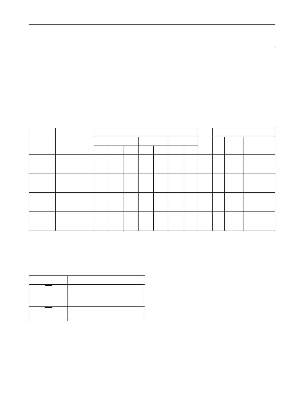
Notes to the HCT DC Characteristics
1. The value of additional quiescent supply current (∆I
) for a unit load of 1 is given in the family specifications.
CC
2. To determine ∆ICC per input, multiply this value by the unit load coefficient shown in the table below.
UNIT LOAD COEFFICIENT
INPUT UNIT LOAD COEFFICIENT
OE 1
SI 1.5
D
n
0.75
MR 1.5
SO 1.5
September 1993 9
 Loading...