

Philips 74HCT73DB, 74HCT73D, 74HCT73U, 74HCT73N, 74HC73U Datasheet
...
DATA SH EET
Product specification
File under Integrated Circuits, IC06
December 1990
INTEGRATED CIRCUITS
74HC/HCT73
Dual JK flip-flop with reset;
negative-edge trigger
For a complete data sheet, please also download:
•The IC06 74HC/HCT/HCU/HCMOS Logic Family Specifications
•The IC06 74HC/HCT/HCU/HCMOS Logic Package Information
•The IC06 74HC/HCT/HCU/HCMOS Logic Package Outlines
December 1990 2
Philips Semiconductors Product specification
Dual JK flip-flop with reset; negative-edge trigger 74HC/HCT73
FEATURES
• Output capability: standard
• ICC category: flip-flops
GENERAL DESCRIPTION
The 74HC/HCT73 are high-speed Si-gate CMOS devices
and are pin compatible with low power Schottky TTL
(LSTTL). They are specified in compliance with JEDEC
standard no. 7A.
The 74HC/HCT73 are dual negative-edge triggered
JK-type flip-flops featuring individual J, K, clock (n
CP) and
reset (nR) inputs; also complementary Q and Q outputs.
The J and K inputs must be stable one set-up time prior to
the HIGH-to-LOW clock transition for predictable
operation.
The reset (nR) is an asynchronous active LOW input.
When LOW, it overrides the clock and data inputs, forcing
the Q output LOW and the Q output HIGH.
Schmitt-trigger action in the clock input makes the circuit
highly tolerant to slower clock rise and fall times.
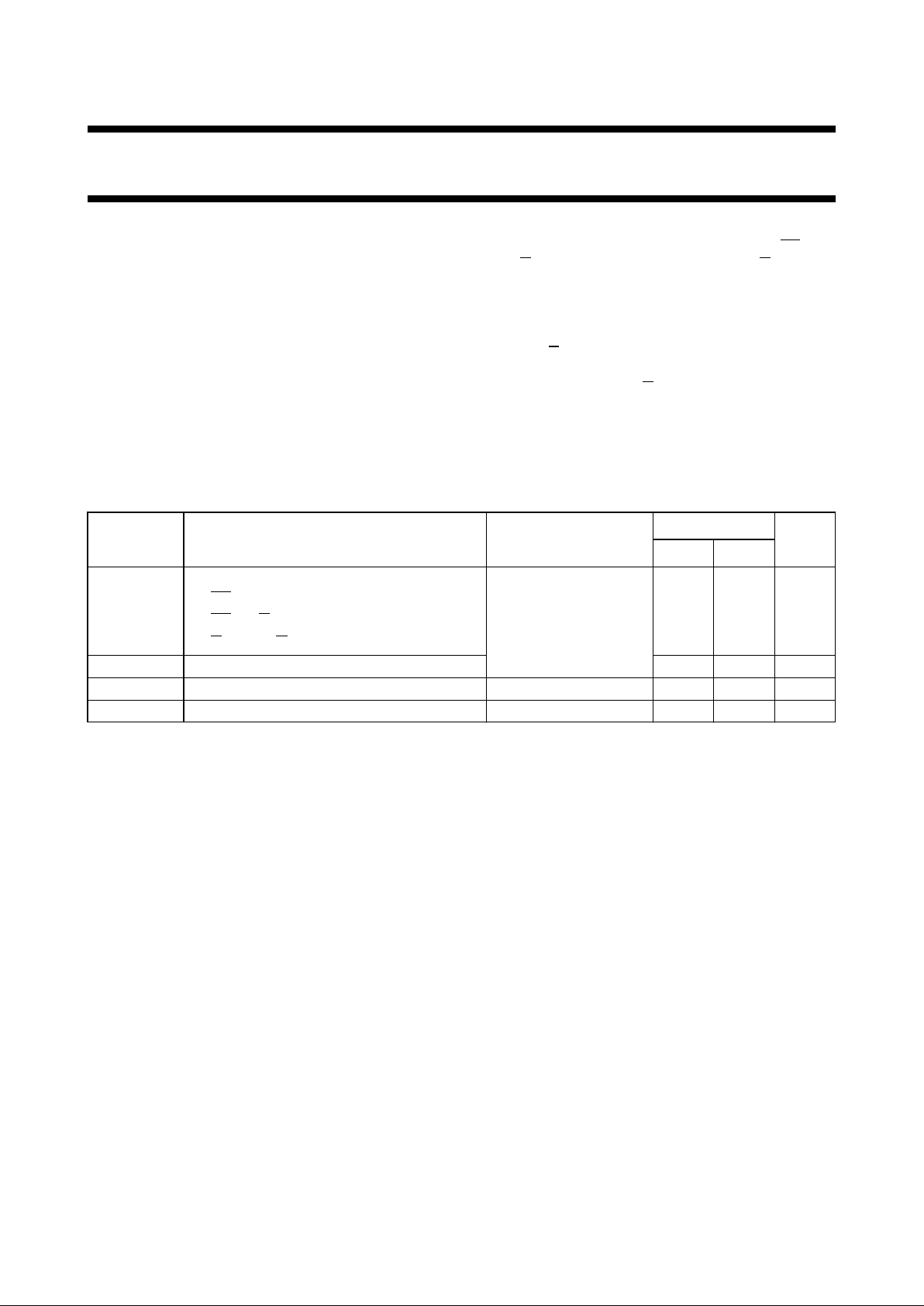
QUICK REFERENCE DATA
GND = 0 V; T
amb
=25°C; tr=tf= 6 ns
Notes
1. C
PD
is used to determine the dynamic power dissipation (PD in µW):
PD=CPD× V
CC
2
× fi+∑(CL× V
CC
2
× fo) where:
fi= input frequency in MHz
fo= output frequency in MHz
∑ (CL× V
CC
2
× fo) = sum of outputs
CL= output load capacitance in pF
VCC= supply voltage in V
2. For HC the condition is VI= GND to V
CC
For HCT the condition is VI= GND to VCC− 1.5 V
ORDERING INFORMATION
See
“74HC/HCT/HCU/HCMOS Logic Package Information”
.
SYMBOL PARAMETER CONDITIONS
TYPICAL
UNIT
HC HCT
t
PHL
/ t
PLH
propagation delay CL= 15 pF; VCC=5 V
n
CP to nQ 16 15 ns
n
CP to nQ 1618ns
n
R to nQ, nQ 1515ns
f
max
maximum clock frequency 77 79 MHz
C
I
input capacitance 3.5 3.5 pF
C
PD
power dissipation capacitance per flip-flop notes 1 and 2 30 30 pF
December 1990 3
Philips Semiconductors Product specification
Dual JK flip-flop with reset; negative-edge trigger 74HC/HCT73
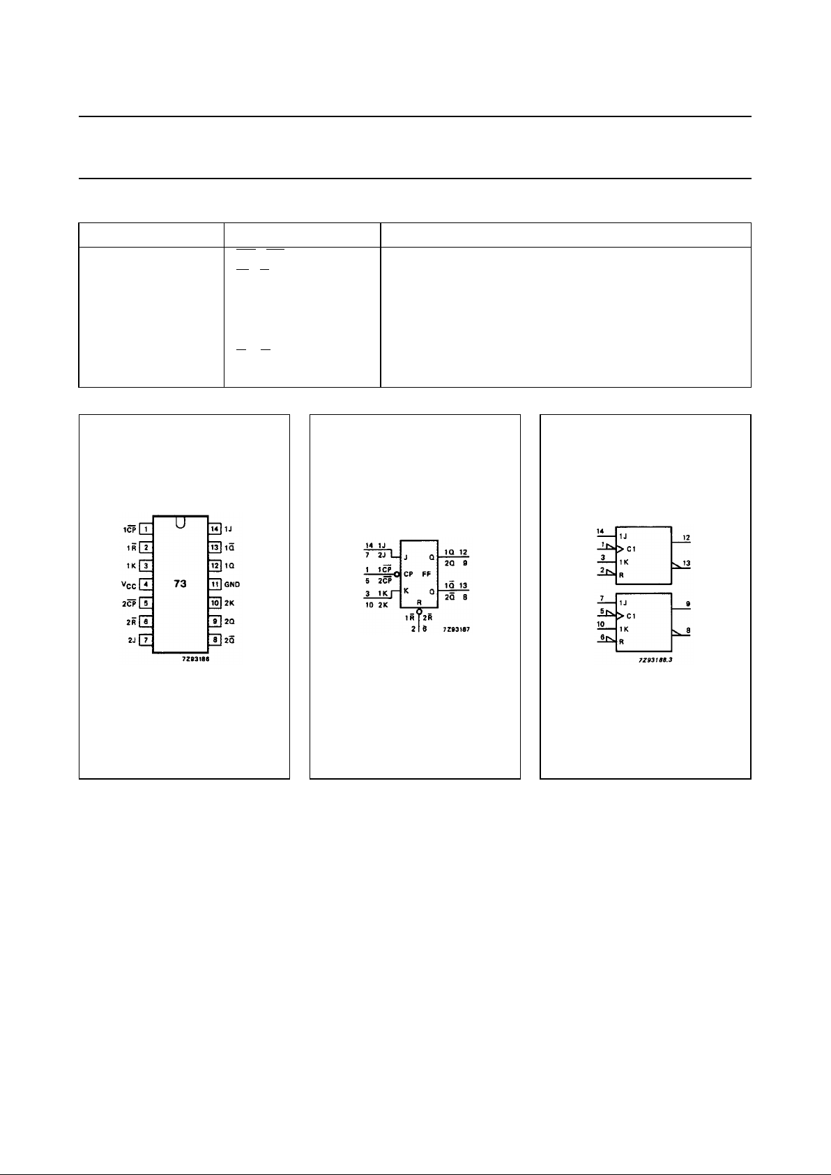
PIN DESCRIPTION
PIN NO. SYMBOL NAME AND FUNCTION
1, 5 1
CP, 2CP clock input (HIGH-to-LOW, edge-triggered)
2, 6 1
R, 2R asynchronous reset inputs (active LOW)
4V
CC
positive supply voltage
11 GND ground (0 V)
12, 9 1Q, 2Q true flip-flop outputs
13, 8 1
Q, 2Q complement flip-flop outputs
14, 7, 3, 10 1J, 2J, 1K, 2K synchronous inputs; flip-flops 1 and 2
Fig.1 Pin configuration. Fig.2 Logic symbol. Fig.3 IEC logic symbol.
 Loading...