

Philips 74HCT688U, 74HCT688PW, 74HCT688NB, 74HCT688N, 74HCT688DB Datasheet
...
DATA SH EET
Product specification
File under Integrated Circuits, IC06
December 1990
INTEGRATED CIRCUITS
74HC/HCT688
8-bit magnitude comparator
For a complete data sheet, please also download:
•The IC06 74HC/HCT/HCU/HCMOS Logic Family Specifications
•The IC06 74HC/HCT/HCU/HCMOS Logic Package Information
•The IC06 74HC/HCT/HCU/HCMOS Logic Package Outlines
December 1990 2
Philips Semiconductors Product specification
8-bit magnitude comparator 74HC/HCT688
FEATURES
• Compare two 8-bit words
• Output capability: standard
• ICCcategory: MSI
GENERAL DESCRIPTION
The 74HC/HCT688 are high-speed Si-gate CMOS devices
and are pin compatible with low power Schottky TTL
(LSTTL). They are specified in compliance with JEDEC
standard no. 7A.
The 74HC/HCT688 are 8-bit magnitude comparators.
They perform comparison of two 8-bit binary or BCD
words.
The output provides P = Q.
QUICK REFERENCE DATA
GND = 0 V; T
amb
=25°C; tr=tf= 6 ns
Notes
1. C
PD
is used to determine the dynamic power dissipation (PD in µW):
PD=CPD× V
CC
2
× fi+ ∑ (CL× V
CC
2
× fo) where:
fi= input frequency in MHz
fo= output frequency in MHz
∑ (CL× V
CC
2
× fo) = sum of outputs
CL= output load capacitance in pF
VCC= supply voltage in V
2. For HC the condition is VI= GND to V
CC
For HCT the condition is VI= GND to VCC− 1.5 V
ORDERING INFORMATION
See
“74HC/HCT/HCU/HCMOS Logic Package Information”
.
SYMBOL PARAMETER CONDITIONS
TYPICAL
UNIT
HC HCT
t
PHL/ tPLH
propagation delay CL= 15 pF; VCC=5 V
P
n
, Qnto P = Q 1717ns
E to
P = Q 8 12 ns
C
I
input capacitance 3.5 3.5 pF
C
PD
power dissipation capacitance per package notes 1 and 2 30 30 pF
December 1990 3
Philips Semiconductors Product specification
8-bit magnitude comparator 74HC/HCT688
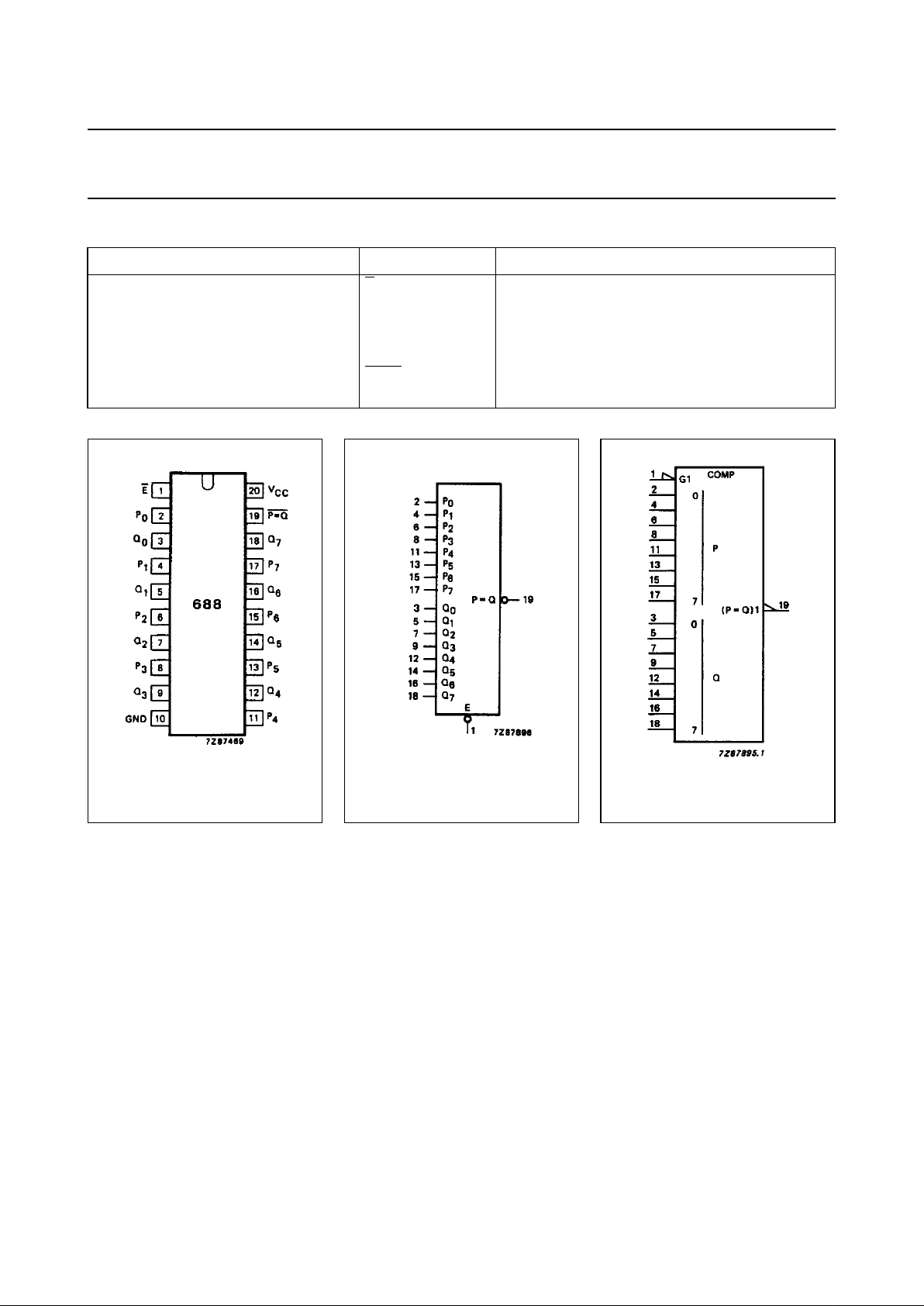
PIN DESCRIPTION
PIN NO. SYMBOL NAME AND FUNCTION
1
E enable input (active LOW)
2, 4, 6, 8, 11, 13, 15, 17 P
0
to P
7
word inputs
3, 5, 7, 9, 12, 14, 16, 18 Q
0
to Q
7
word inputs
10 GND ground (0 V)
19
P = Q equal to output
20 V
CC
positive supply voltage
Fig.1 Pin configuration. Fig.2 Logic symbol. Fig.3 IEC logic symbol.
 Loading...