

Philips 74HCT157U, 74HCT157PW, 74HCT157N, 74HCT157DB, 74HC157U Datasheet
...
DATA SH EET
Product specification
File under Integrated Circuits, IC06
December 1990
INTEGRATED CIRCUITS
74HC/HCT157
Quad 2-input multiplexer
For a complete data sheet, please also download:
•The IC06 74HC/HCT/HCU/HCMOS Logic Family Specifications
•The IC06 74HC/HCT/HCU/HCMOS Logic Package Information
•The IC06 74HC/HCT/HCU/HCMOS Logic Package Outlines
December 1990 2
Philips Semiconductors Product specification
Quad 2-input multiplexer 74HC/HCT157
FEATURES
• Non-inverting data path
• Output capability: standard
• ICCcategory: MSI
GENERAL DESCRIPTION
The 74HC/HCT157 are high-speed Si-gate CMOS devices
and are pin compatible with low power Schottky TTL
(LSTTL). They are specified in compliance with JEDEC
standard no. 7A.
The 74HC/HCT157 are quad 2-input multiplexers which
select 4 bits of data from two sources under the control of
a common data select input (S). The four outputs present
the selected data in the true (non-inverted) form. The
enable input (
E) is active LOW. When E is HIGH, all of the
outputs (1Y to 4Y) are forced LOW regardless of all other
input conditions.
Moving the data from two groups of registers to four
common output buses is a common use of the “157”. The
state of the common data select input (S) determines the
particular register from which the data comes. It can also
be used as function generator.
The device is useful for implementing highly irregular logic
by generating any four of the 16 different functions of two
variables with one variable common.
The “157” is the logic implementation of a 4-pole,
2-position switch, where the position of the switch is
determined by the logic levels applied to S.
The logic equations are:
1Y = E.(1l1.S + 1l0.S)
2Y = E.(2l1.S + 2l0.S)
3Y = E.(3l1.S + 3l0.S)
4Y = E.(4l1.S + 4l0.S)
The “157” is identical to the “158” but has non-inverting
(true) outputs.
QUICK REFERENCE DATA
GND = 0 V; T
amb
= 25 °C; tr= tf= 6 ns
Notes
1. C
PD
is used to determine the dynamic power dissipation (PDin µW):
PD= CPD× V
CC
2
× fi+ ∑ (CL× V
CC
2
× fo) where:
fi= input frequency in MHz
fo= output frequency in MHz
∑ (CL× V
CC
2
× fo) = sum of outputs
CL= output load capacitance in pF
VCC= supply voltage in V
2. For HC the condition is VI= GND to V
CC
For HCT the condition is VI= GND to VCC− 1.5 V
ORDERING INFORMATION
See
“74HC/HCT/HCU/HCMOS Logic Package Information”
.
SYMBOL PARAMETER CONDITIONS
TYPICAL
UNIT
HC HCT
t
PHL
/ t
PLH
propagation delay CL= 15 pF; VCC= 5 V
nI
0
, nI1to nY 11 13 ns
E to nY 11 12 ns
S to nY 12 19 ns
C
I
input capacitance 3.5 3.5 pF
C
PD
power dissipation capacitance per multiplexer notes 1 and 2 70 70 pF
December 1990 3
Philips Semiconductors Product specification
Quad 2-input multiplexer 74HC/HCT157
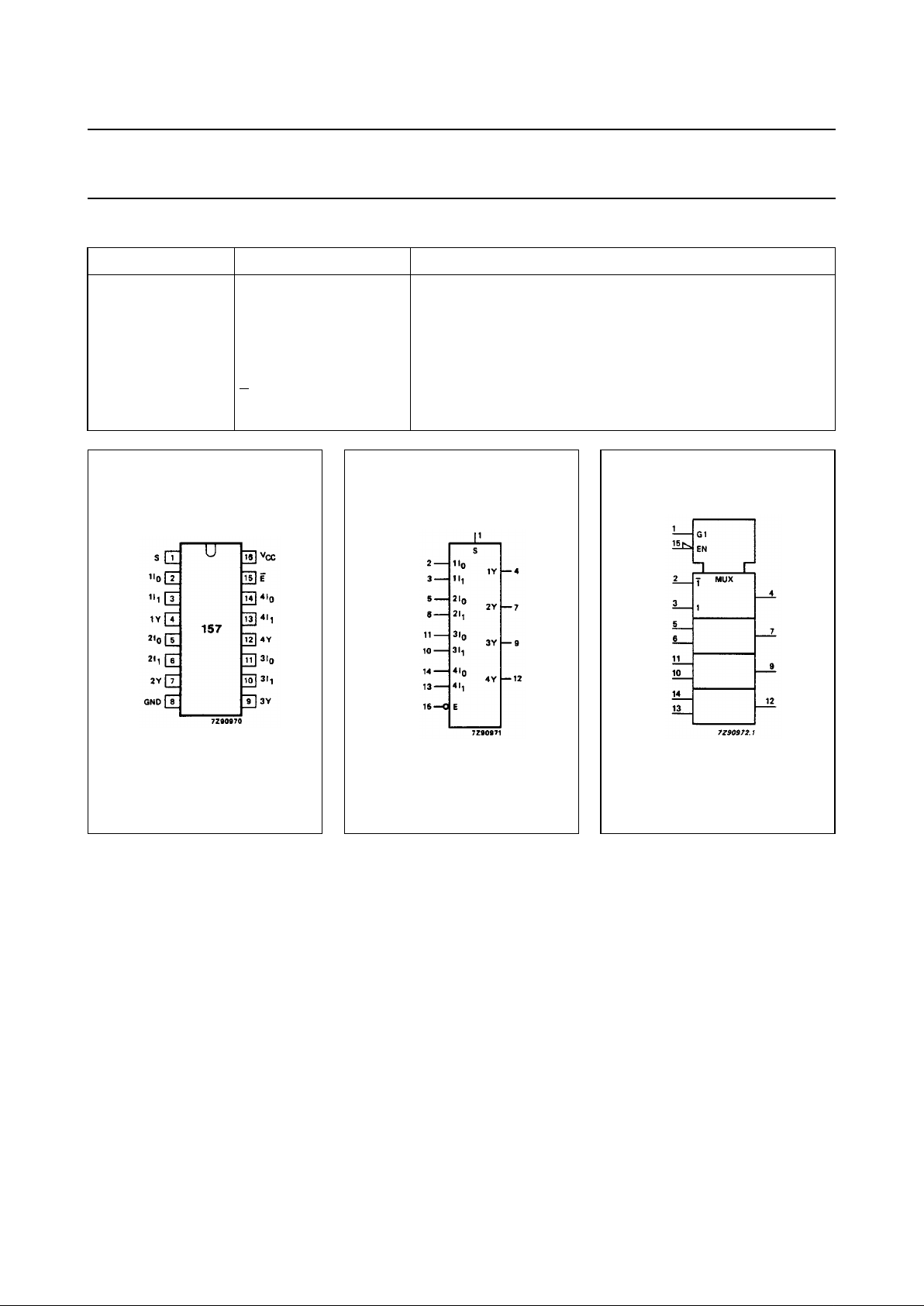
PIN DESCRIPTION
PIN NO. SYMBOL NAME AND FUNCTION
1 S common data select input
2, 5, 11, 14 1I
0
to 4I
0
data inputs from source 0
3, 6, 10, 13 1I
1
to 4I
1
data inputs from source 1
4, 7, 9, 12 1Y to 4Y multiplexer outputs
8 GND ground (0 V)
15
E enable input (active LOW)
16 V
CC
positive supply voltage
Fig.1 Pin configuration. Fig.2 Logic symbol. Fig.3 IEC logic symbol.
 Loading...