

Philips 74ABT374APW, 74ABT374AN, 74ABT374ADB, 74ABT374AD Datasheet

Philips Semiconductors Product specification
Octal D-type flip-flop; positive-edge trigger
(3-State)
FEA TURES
•8-bit positive edge triggered register
•3-State output buffers
•Output capability: +64mA/–32mA
•Latch-up protection exceeds 500mA per Jedec Std 17
•ESD protection exceeds 2000 V per MIL STD 883 Method 3015
and 200 V per Machine Model
•Power-up 3-State
•Power-up reset
•Live insertion/extraction permitted
QUICK REFERENCE DAT A
SYMBOL PARAMETER
C
t
PLH
t
PHL
C
OUT
I
CCZ
IN
Propagation delay
CP to Qn
Input capacitance VI = 0V or V
Output capacitance Outputs disabled; VO = 0V or V
Total supply current Outputs disabled; VCC =5.5V 110 µA
CL = 50pF; VCC = 5V
DESCRIPTION
The 74ABT374A high-performance BiCMOS device combines low
static and dynamic power dissipation with high speed and high
output drive.
The 74ABT374A is an 8-bit, edge triggered register coupled to eight
3-State output buffers. The two sections of the device are controlled
independently by the clock (CP) and Output Enable (OE
gates.
The register is fully edge triggered. The state of each D input, one
set-up time before the Low-to-High clock transition, is transferred to
the corresponding flip-flop’s Q output.
The 3-State output buffers are designed to drive heavily loaded
3-State buses, MOS memories, or MOS microprocessors. The
active-Low Output Enable (OE
independent of the clock operation.
When OE
is High, the outputs are in the High-impedance “OFF” state, which
means they will neither drive nor load the bus.
T
is Low, the stored data appears at the outputs. When OE
CONDITIONS
= 25°C; GND = 0V
amb
CC
CC
74ABT374A
) control
) controls all eight 3-State buffers
TYPICAL UNIT
3.4
3.8
4 pF
7 pF
ns
ORDERING INFORMATION
PACKAGES TEMPERATURE RANGE OUTSIDE NORTH AMERICA NORTH AMERICA DWG NUMBER
20-Pin Plastic DIP –40°C to +85°C 74ABT374A N 74ABT374A N SOT146-1
20-Pin plastic SO –40°C to +85°C 74ABT374A D 74ABT374A D SOT163-1
20-Pin Plastic SSOP Type II –40°C to +85°C 74ABT374A DB 74ABT374A DB SOT339-1
20-Pin Plastic TSSOP Type I –40°C to +85°C 74ABT374A PW 74ABT374APW DH SOT360-1
PIN CONFIGURA TION
1
OE
2
Q0
3
D0
4
D1
5
Q1
6
Q2
7
D2
8
D3
9
Q3 Q4
10 11
GND
20
V
CC
Q7
19
D7
18
D6
17
Q6
16
Q5
15
D5
14
D4
13
12
CP
SA00110
PIN DESCRIPTION
PIN
NUMBER
1 OE Output enable input (active-Low)
3, 4, 7, 8,
13, 14, 17,
18
2, 5, 6, 9,
12, 15, 16,
19
11 CP Clock pulse input (active rising edge)
10 GND Ground (0V)
20 V
SYMBOL FUNCTION
D0-D7 Data inputs
Q0-Q7 Data outputs
Positive supply voltage
CC
1995 Sep 06 853-1448 15704
1
Philips Semiconductors Product specification
INTERNAL
OPERATING MODE
Latch
Disabl
Octal D-type flip-flop; positive-edge trigger
(3-State)
LOGIC SYMBOL
3 4 7 8 13 14 1817
D0 D1 D2 D3 D4 D5 D6 D7
CP
11
OE
1
Q0 Q1 Q2 Q3 Q4 Q5 Q6 Q7
2 5 6 9 12 15 16 19
SA00111
FUNCTION TABLE
INPUTS
OE CP Dn
INTERNAL
REGISTER
L ↑ l L L
L ↑ h H H
L ↑ X NC NC Hold
H ↑ X NC Z
H ↑ Dn Dn Z
H = High voltage level
h = High voltage level one set-up time prior to the Low-to-High clock transition
L = Low voltage level
l = Low voltage level one set-up time prior to the Low-to-High clock transition
NC= No change
X = Don’t care
Z = High impedance “off” state
↑ = Low-to-High clock transition
= not a Low-to-High clock transition
↑
OUTPUTS
Q0 – Q7
LOGIC SYMBOL (IEEE/IEC)
and read register
e outputs
74ABT374A
1
11
32
45
76
89
13 12
14 15
17 16
18 19
EN
C1
1D
SA00112
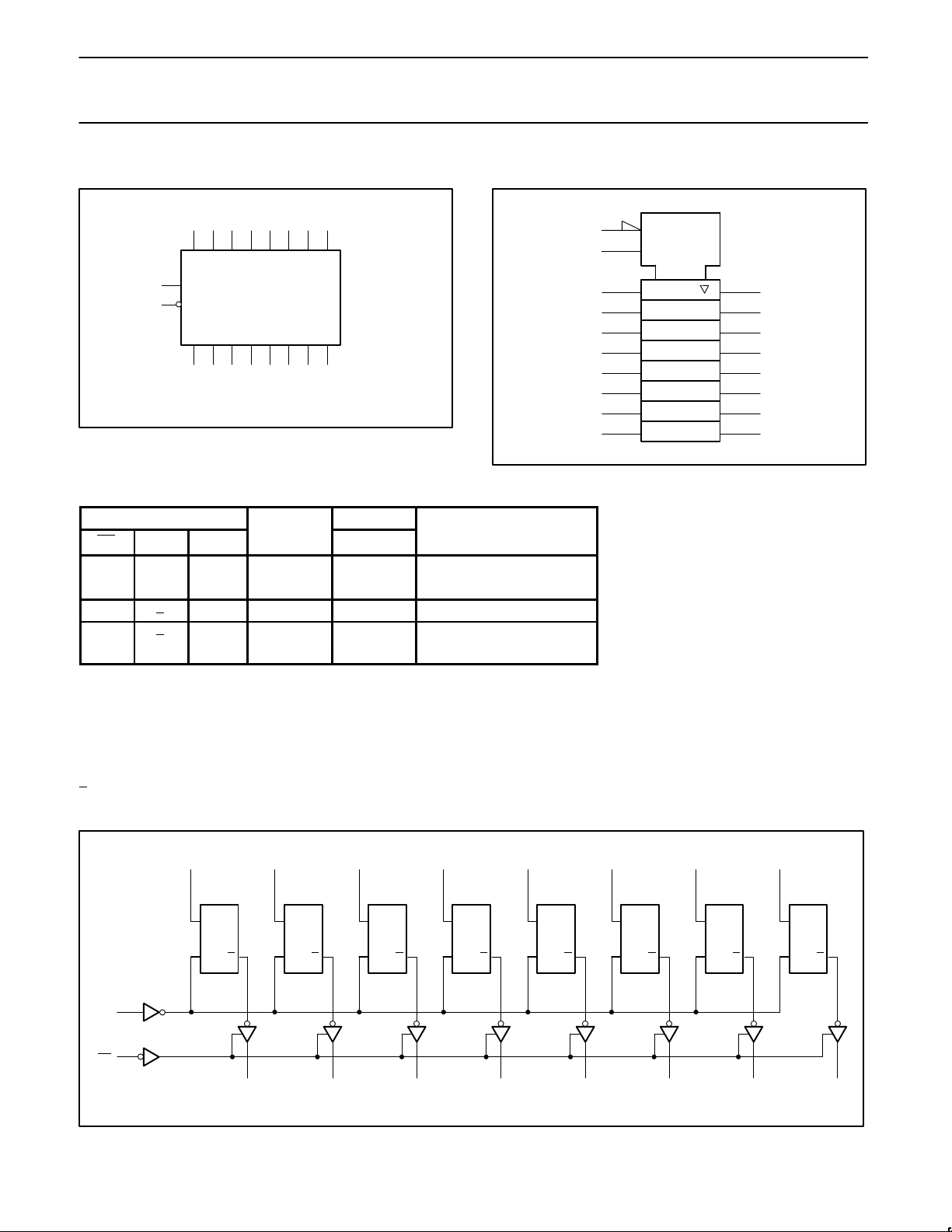
LOGIC DIAGRAM
D0
11
CP
1
OE
1995 Sep 06
D1
3 4 7 8 13 14 17 18
D
CP Q
Q0
D
CP Q
2 5 6 9 12 15 16 19
D2
D
CP Q
Q1 Q2 Q3 Q4 Q5 Q6 Q7
D3
D
CP Q
D4
D
CP Q
D5
D
CP Q
D6
D
CP Q
D7
2
D
CP Q
SA00113
 Loading...