

Philips 74abt2952 DATASHEETS

INTEGRATED CIRCUITS
74ABT2952
Octal registered transceiver (3-State)
Product specification
Supersedes data of 1995 Jun 15
IC23 Data Handbook
1998 Feb 11
Philips Semiconductors Product specification
74ABT2952Octal registered transceiver (3-State)
FEA TURES
•8-bit registered transceiver
•Independent registers for A and B buses
•Output capability: +64mA/–32mA
•Latch-up protection exceeds 500mA per JEDEC Std 17
•ESD protection exceeds 2000V per MIL STD 883 Method 3015
and 200V per Machine Model
•Power-up 3-State
•Power-up reset
DESCRIPTION
The 74ABT2952 high-performance BiCMOS device combines low
static and dynamic power dissipation with high speed and high
output drive.
The 74ABT2952 device is an 8-bit registered transceiver. Two 8-bit
back-to-back registers store data flowing in both directions between
two bidirectional buses. Data applied to the inputs is entered and
stored on the rising edge of the Clock (CPXX) provided that the
Clock Enable (CEXX
output buffers, but is only accessible when the Output Enable
(OEXX) is Low. Data flow from A inputs to B outputs is the same as
for B inputs to A outputs.
) is Low. The data is then present at the 3-State
•Live insertion/extraction permitted
QUICK REFERENCE DATA
SYMBOL PARAMETER
t
PLH
t
PHL
C
C
I
CCZ
IN
I/O
Propagation delay
CPBA to An or
CL = 50pF; VCC = 5V 5.7 ns
CPAB to Bn
Input capacitance VI = 0V or V
I/O capacitance Outputs disabled; VO = 0V or V
Total supply current Outputs disabled; VCC =5.5V 110 µA
ORDERING INFORMATION
PACKAGES TEMPERATURE RANGE OUTSIDE NORTH AMERICA NORTH AMERICA DWG NUMBER
24-Pin Plastic DIP –40°C to +85°C 74ABT2952 N 74ABT2952 N SOT222-1
24-Pin plastic SO –40°C to +85°C 74ABT2952 D 74ABT2952 D SOT137-1
24-Pin Plastic SSOP Type II –40°C to +85°C 74ABT2952 DB 74ABT2952 DB SOT340-1
24-Pin Plastic TSSOP Type I –40°C to +85°C 74ABT2952 PW 7ABT2952PW DH SOT355-1
CONDITIONS
T
= 25°C; GND = 0V
amb
CC
CC
TYPICAL UNIT
4 pF
7 pF
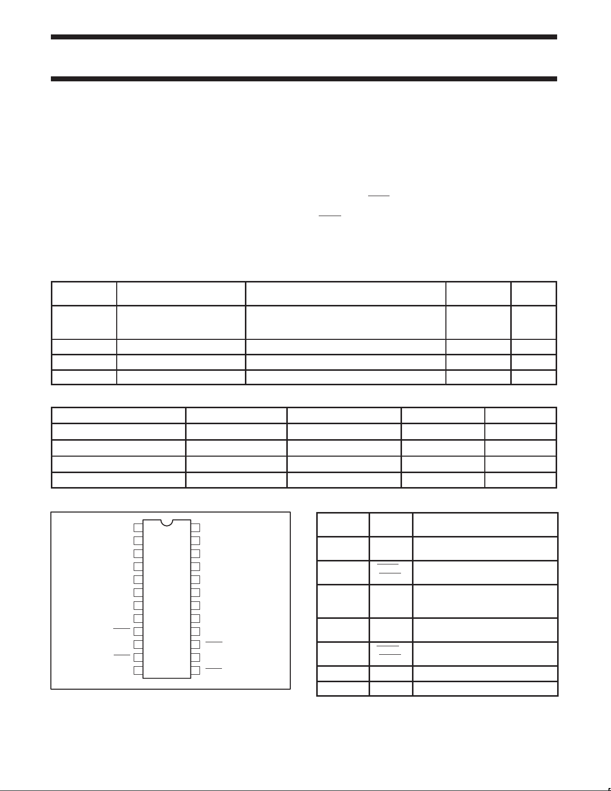
PIN CONFIGURATION
V
1
B7
2
B6
3
B5
4
B4
5
B3
6
B2
7
B1
8
B0
9
OEAB
10 15
CPAB
11 14CEAB
12 13GND
1998 Feb 1 1 853-1554 18949
24
23
22
21
20
19
18
17
16
SA00114
CC
A7
A6
A5
A4
A3
A2
A1
A0
OEBA
CPBA
CEBA
PIN DESCRIPTION
PIN
NUMBER
10, 14
11, 13
16, 17, 18,
19, 20, 21,
22, 23
1, 2, 3, 4, 5,
6, 7, 8
9, 15
12 GND Ground (0V)
24 V
2
SYMBOL NAME AND FUNCTION
CPAB /
CPBA
CEAB /
CEBA
Clock input A to B / Clock input B to A
Clock enable input A to B / Clock
enable input B to A
A0 – A7 Data inputs/outputs (A side)
B0 – B7 Data outputs/outputs (B side)
OEAB /
OEBA
Output enable inputs
Positive supply voltage
CC
Philips Semiconductors Product specification
74ABT2952Octal registered transceiver (3-State)
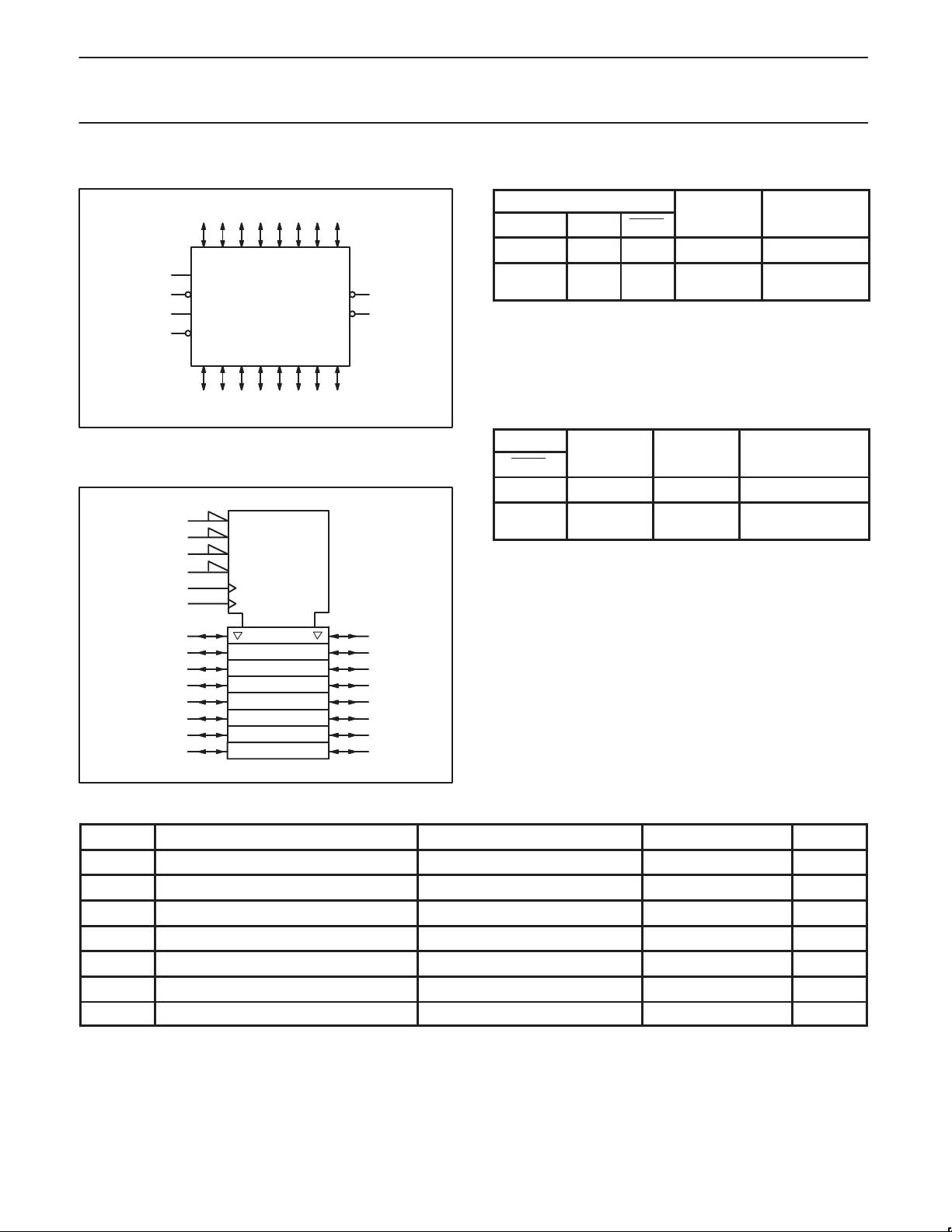
LOGIC SYMBOL
16 17 18 19 20 21 22 23
A0 A1 A2 A3 A4 A5 A6 A7
10
CPAB
11
CEAB
14
CPBA
13
CEBA
B0 B1 B2 B3 B4 B5 B6 B7
87654321
LOGIC SYMBOL (IEEE/IEC)
11
13
15
9
10
14
EN1
EN2
EN3
EN4
C5
C6
OEBA
OEAB
SA00115
FUNCTION TABLE for Register An or Bn
INPUTS
An or Bn CPXX CEXX
X X H NC Hold data
L
15
9
H
H = High voltage level
↑
↑
L =Low voltage level
↑ =Low–to–High transition
X = Don’t care
XX= AB or BA
NC=No change
INTERNAL OPERATING
Q MODE
L
L
L
H
Load data
FUNCTION TABLE for Output Enable
INPUTS
OEXX
H X Z Disable outputs
L
L
H = High voltage level
L =Low voltage level
X = Don’t care
XX= AB or BA
Z =High impedance “off” state
INTERNAL An or Bn OPERATING
Q OUTPUTS MODE
L
H
L
H
Enable outputs
16
17
18
19
20
21
22
23
1, 4, 52, 3, 6
ABSOLUTE MAXIMUM RATINGS
SYMBOL
V
CC
I
IK
V
I
I
OK
V
OUT
I
OUT
T
stg
DC supply voltage –0.5 to +7.0 V
DC input diode current VI < 0 –18 mA
DC input voltage
DC output diode current VO < 0 –50 mA
DC output voltage
DC output current output in Low state 128 mA
Storage temperature range –65 to 150 °C
PARAMETER CONDITIONS RATING UNIT
3
3
1, 2
8
7
6
5
4
3
2
1
SA00116
–1.2 to +7.0 V
output in Off or High state –0.5 to +5.5 V
NOTES:
1. Stresses beyond those listed may cause permanent damage to the device. These are stress ratings only and functional operation of the
device at these or any other conditions beyond those indicated under “recommended operating conditions” is not implied. Exposure to
absolute-maximum-rated conditions for extended periods may affect device reliability .
2. The performance capability of a high-performance integrated circuit in conjunction with its thermal environment can create junction
temperatures which are detrimental to reliability. The maximum junction temperature of this integrated circuit should not exceed 150°C.
3. The input and output voltage ratings may be exceeded if the input and output current ratings are observed.
1998 Feb 1 1
3
Philips Semiconductors Product specification
SYMBOL
PARAMETER
UNIT
74ABT2952Octal registered transceiver (3-State)
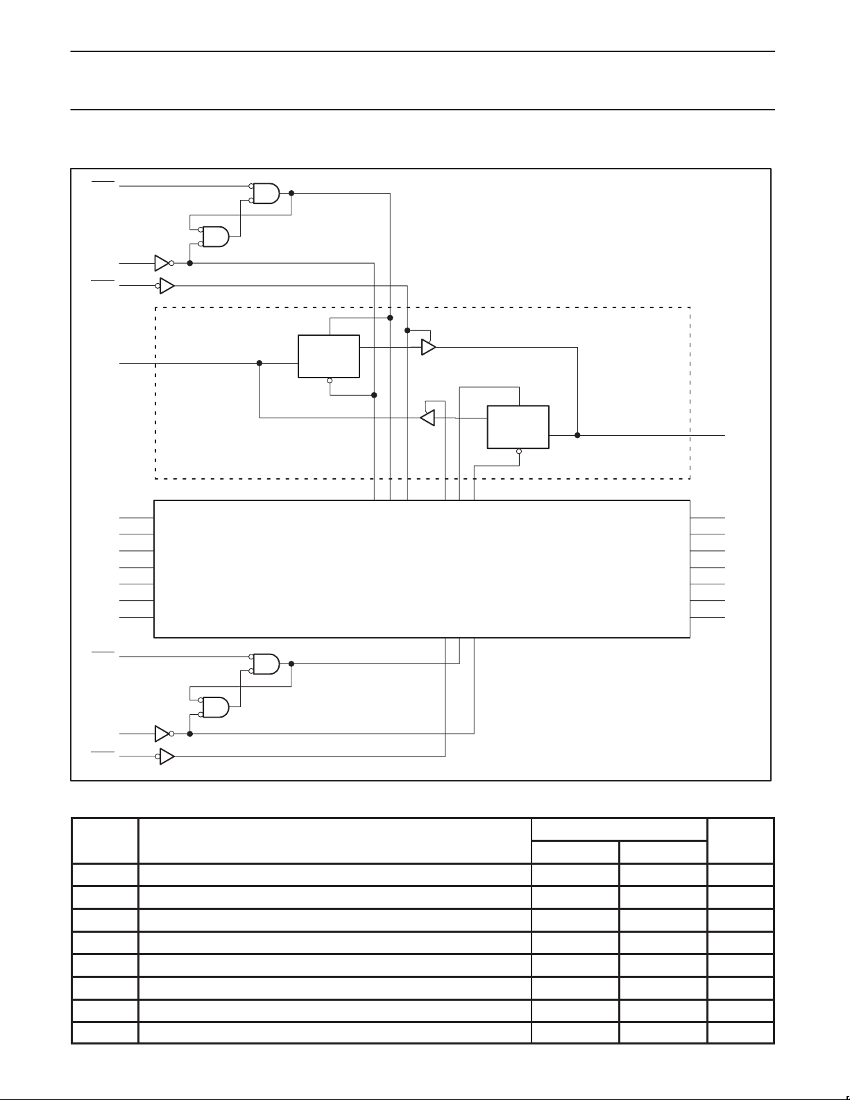
LOGIC DIAGRAM
11
CEAB
10
CPAB
9
OEAB
DETAIL A
CE
CP
Q
CE
Q
D
CP
8
B0
16
A0
D
17
A1
18
A2
19
A3
CEBA
CPBA
OEBA
20
A4
21
A5
22
A6
23
A7
13
14
15
DETAIL A X 7
RECOMMENDED OPERATING CONDITIONS
LIMITS
Min Max
V
CC
V
V
V
I
OH
I
OL
∆t/∆v Input transition rise or fall rate 0 10 ns/V
T
amb
DC supply voltage 4.5 5.5 V
Input voltage 0 V
I
High-level input voltage 2.0 V
IH
Low-level Input voltage 0.8 V
IL
High-level output current –32 mA
Low-level output current 64 mA
Operating free-air temperature range –40 +85 °C
CC
7
B1
6
B2
5
B3
4
B4
3
B5
2
B6
1
B7
SA00117
V
1998 Feb 1 1
4
 Loading...