

Philips 74ABT273APW, 74ABT273AN, 74ABT273ADB, 74ABT273AD Datasheet
INTEGRATED CIRCUITS
74ABT273A
Octal D-type flip-flop
Product specification 1995 Sep 06
IC23 Data Handbook
Philips Semiconductors Product specification
74ABT273AOctal D-type flip-flop
FEA TURES
•Eight edge-triggered D-type flip-flops
•Buffered common clock
•Buffered asynchronous Master Reset
•Power-up reset
•See 74ABT377 for clock enable version
•See 74ABT373 for transparent latch version
•See 74ABT374 for 3-State version
•ESD protection exceeds 2000 V per Mil Std 833 Method 3015 and
DESCRIPTION
The 74ABT273A has eight edge-triggered D-type flip-flops with
individual D inputs and Q outputs. The common buffered Clock (CP)
and Master Reset (MR
simultaneously .
The register is fully edge-triggered. The state of each D input, one
setup time before the Low-to-High clock transition, is transferred to
the corresponding flip-flop’s Q output.
All outputs will be forced Low independent of Clock or Data inputs
by a Low voltage level on the MR
applications where the true output only is required and the CP and
MR
are common elements.
) inputs load and reset (clear) all flip-flops
input. The device is useful for
200 V per machine model.
QUICK REFERENCE DATA
SYMBOL PARAMETER
t
PLH
t
PHL
C
I
CCH
IN
Propagation delay
CP to Qn
Input capacitance VI = 0V or V
Total supply current Outputs High; VCC =5.5V 150 µA
CL = 50pF; VCC = 5V
CONDITIONS
= 25°C; GND = 0V
T
amb
CC
TYPICAL UNIT
3.0
3.4
3.5 pF
ORDERING INFORMATION
PACKAGES TEMPERATURE RANGE OUTSIDE NORTH AMERICA NORTH AMERICA DWG NUMBER
20-Pin Plastic DIP –40°C to +85°C 74ABT273A N 74ABT273A N SOT146-1
20-Pin plastic SO –40°C to +85°C 74ABT273A D 74ABT273A D SOT163-1
20-Pin Plastic SSOP Type II –40°C to +85°C 74ABT273A DB 74ABT273A DB SOT339-1
20-Pin Plastic TSSOP Type I –40°C to +85°C 74ABT273A PW 7ABT273APW DH SOT360-1
ns
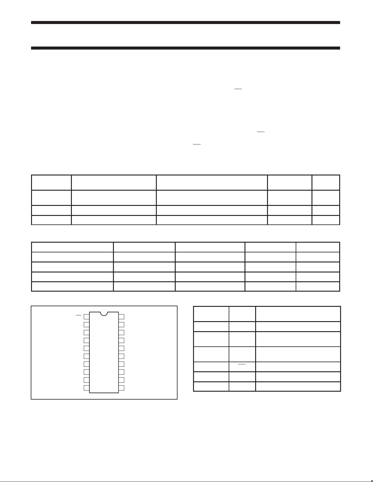
PIN CONFIGURATION
1
MR
2
Q0
3
D0
4
D1
5
Q1
6
Q2
7
D2
8
D3
9
Q3 Q4
10 11
GND
1995 Sep 06 853-1774 15704
20
V
CC
19
Q7
18
D7
17
D6
16
Q6
15
Q5
14
D5
13
D4
12
CP
SA00052
PIN DESCRIPTION
PIN
NUMBER
11 CP Clock pulse input (active rising edge)
3, 4, 7, 8, 13,
14, 17, 18
2, 5, 6, 9, 12,
15, 16, 19
1 MR Master Reset input (active-Low)
10 GND Ground (0V)
20 V
2
SYMBOL NAME AND FUNCTION
D0 - D7 Data inputs
Q0 - Q7 Data outputs
Positive supply voltage
CC
Philips Semiconductors Product specification
OPERATING MODE
74ABT273AOctal D-type flip-flop
LOGIC SYMBOL (IEEE/IEC)
1
11
32
45
76
89
13 12
14 15
17 16
18 19
R
C1
1D
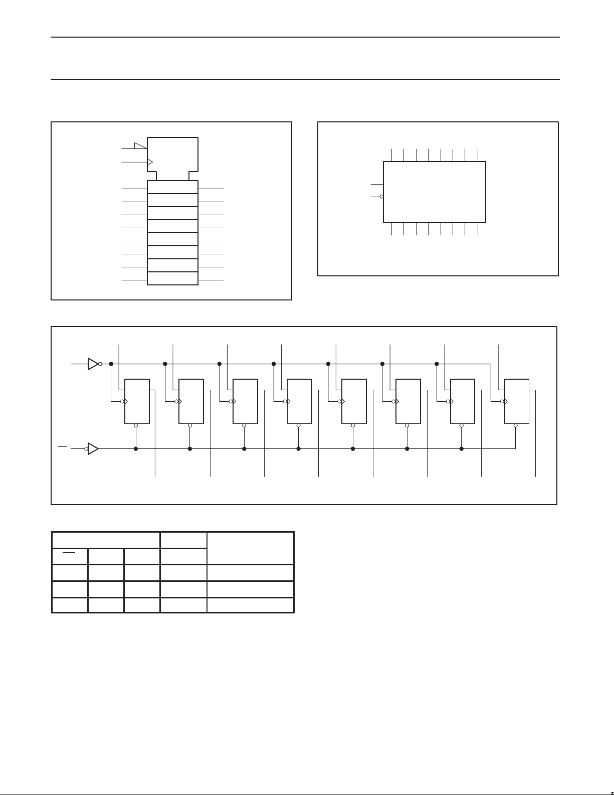
LOGIC DIAGRAM
CP
D0
11
3
D
CP
R
D
D1
Q
LOGIC SYMBOL
3 4 7 8 13 14 1817
D0 D1 D2 D3 D4 D5 D6 D7
11
CP
1
MR
Q0 Q1 Q2 Q3 Q4 Q5 Q6 Q7
2 5 6 9 12 15 16 19
SA00053
SA00054
D2
4
D
Q
CP
R
D
7
D
CP
R
D
D3
8
Q
D
CP
R
D
D4
13
Q
D
CP
R
D
D5
14
Q
D
CP
R
D
D6
17
Q
D
CP
R
D
D7
18
Q
D
Q
CP
R
D
1
MR
Q0
2
5
Q1
6
Q2
FUNCTION TABLE
INPUTS OUTPUTS
MR CP Dn Q0 - Q7
L X X L Reset (clear)
H ↑ h H Load ”1”
H ↑ l L Load ”0”
H = High voltage level
h = High voltage level one set-up time prior to the Low-to-High
clock transition
L = Low voltage level
l = Low voltage level one set-up time prior to the Low-to-High
clock transition
X = Don’t care
↑ = Low-to-High clock transition
Q3
9
Q4
12
Q5
15
Q6
16
19
Q7
SA00055
1995 Sep 06
3

Philips Semiconductors Product specification
SYMBOL
PARAMETER
UNIT
74ABT273AOctal D-type flip-flop
ABSOLUTE MAXIMUM RATINGS
SYMBOL
V
CC
I
IK
V
I
I
OK
V
OUT
I
OUT
T
stg
DC supply voltage -0.5 to +7.0 V
DC input diode current VI < 0 -18 mA
DC input voltage
DC output diode current VO < 0 -50 mA
DC output voltage
DC output current output in Low state 128 mA
Storage temperature range -65 to 150 °C
PARAMETER CONDITIONS RATING UNIT
3
3
1, 2
-1.2 to +7.0 V
output in Off or High state -0.5 to +5.5 V
NOTES:
1. Stresses beyond those listed may cause permanent damage to the device. These are stress ratings only and functional operation of the
device at these or any other conditions beyond those indicated under “recommended operating conditions” is not implied. Exposure to
absolute-maximum-rated conditions for extended periods may affect device reliability .
2. The performance capability of a high-performance integrated circuit in conjunction with its thermal environment can create junction
temperatures which are detrimental to reliability. The maximum junction temperature of this integrated circuit should not exceed 150°C.
3. The input and output voltage ratings may be exceeded if the input and output current ratings are observed.
RECOMMENDED OPERATING CONDITIONS
LIMITS
Min Max
V
CC
V
V
V
I
OH
I
OL
∆t/∆v Input transition rise or fall rate 0 10 ns/V
T
amb
DC supply voltage 4.5 5.5 V
Input voltage 0 V
I
High-level input voltage 2.0 V
IH
Low-level input voltage 0.8 V
IL
High-level output current -32 mA
Low-level output current 64 mA
Operating free-air temperature range -40 +85 °C
CC
V
1995 Sep 06
4
 Loading...