

Philips 26PF5321/10, 32PF5321/12, 26PF5321/12, 32PF5321/10, 37PF5321/10 Service Manual
...
Colour Television Chassis
LC4.31E
AA
G_16212_000.eps
191006
ME5FL
ME5P
ME6
Contents Page Contents Page
1. Technical Specifications, Connections, and Chassis
Overview 2
2. Safety Instructions, Warnings, and Notes 5
3. Directions for Use 6
4. Mechanical Instructions 7
5. Service Modes, Error Codes, and Fault Finding 12
6. Block Diagrams, Test Point Overviews, and
Waveforms
Wiring Diagram 26" & 32" 21
Wiring Diagram 37" 22
Wiring Diagram 42" 23
Block Diagram Supply 37" 24
Block Diagram Supply 42" 25
Block Diagram Video 26
Block Diagram Audio 27
Keyboard Control Board (26" & 32") (E) 121 121
Keyboard Control Board (37" & 42") (E) 122 122
Front IR / LED Panel (26" & 32") (ME5P) (J) 123 123
IR-LED and Light Sensor Panel (26"& 32") (J) 124 124
Front IR / LED Panel (37" & 42") (J) 125 126
Standby & Audio Panel: Connections (SA1) 127 130-132
Standby & Audio Panel: Standby (SA2)128 130-132
Standby & Audio Panel: Audio (SA3) 129 130-132
OTC Flash (For 1000pg TXT) (T) 133 134
8. Alignments 135
9. Circuit Descriptions, Abbreviation List, and IC Data
Sheets 140
Abbreviation List 141
IC Data Sheets 144
10. Spare Parts List & CTN Overview 148

Technical Specifications, Connections, and Chassis Overview
EN 2 LC4.31E AA1.
1. Technical Specifications, Connections, and Chassis Overview
Index of this chapter:
1.1 Technical Specifications
1.2 Connection Overview
1.3 Chassis Overview
Notes:
• Figures can deviate due to the different set executions.
• Specifications are indicative (subject to change).
1.1 Technical Specifications
1.1.1 Vision
Display type : LCD, IPS
Screen size :
- 26PF5321/10/12 : 26" (66 cm), 16:9
- 32PF5321/10/12 : 32" (82 cm), 16:9
- 37PF5321/10/12 : 37" (94 cm), 16:9
- 26PF7321/12 : 26" (66 cm), 16:9
- 32PF7321/12 : 32" (82 cm), 16:9
- 37PF7321/10/12 : 37" (94 cm), 16:9
- 42PF5421/10 : 42" (107 cm), 16:9
Resolution (H × V pixels) : 1366 × 768
Contrast ratio :
- 26PF5321/10/12 : 1200:1
- 32PF5321/10/12 : 1200:1
- 37PF5321/10/12 : 1200:1
- 26PF7321/12 : 2400:1
- 32PF7321/12 : 2400:1
- 37PF7321/10/12 : 2400:1
- 42PF5421/10 : 4000:1
Light output (cd/m
2
) : 500
Presets/channels : 100 presets
Tuner bands : VHF
:UHF
: S-band
: Hyper-band
1.1.2 Sound
Sound systems : NICAM B/G, D/K, I, L
: AV Stereo
Maximum power (W
RMS
):
- 26PF5321/10/12 : 2 × 5
- 32PF5321/10/12 : 2 × 15
- 37PF5321/10/12 : 2 × 15
- 26PF7321/12 : 2 × 5
- 32PF7321/12 : 2 × 15
- 37PF7321/10/12 : 2 × 15
- 42PF5421/10 : 2 × 15
1.1.3 Miscellaneous
Power supply:
Mains voltage (V
AC
):
- 26PF5321/10/12 : 110 - 240
- 32PF5321/10/12 : 110 - 240
- 37PF5321/10/12 : 220 - 240
- 26PF7321/12 : 110 - 240
- 32PF7321/12 : 110 - 240
- 37PF7321/10/12 : 220 - 240
- 42PF5421/10 : 220 - 240
Mains frequency (Hz) : 50 / 60
Ambient conditions:
- Temperature range (°C) : +5 to +40
- Maximum humidity : 90% R.H.

Technical Specifications, Connections, and Chassis Overview
EN 3LC4.31E AA 1.
- 26PF7321/12 : 13.0
- 32PF7321/12 : 19.2
- 37PF7321/10/12 : 25.9
- 42PF5421/10 : 31.5
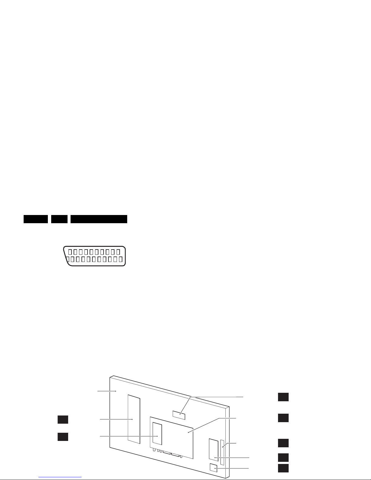
1.2 Connection Overview
Note: The following connector colour abbreviations are used
(acc. to DIN/IEC 757): Bk= Black, Bu= Blue, Gn= Green, Gy=
Grey, Rd= Red, Wh= White, and Ye= Yellow.
1.2.1 Side I/O connections
Figure 1-1 Side I/O connections
S-Video (Hosiden): Video Y/C - In
1 - Ground Y Gnd H
2 - Ground C Gnd H
3 - Video Y 1 V
PP
/ 75 Ω j
4 - Video C 0.3 V
PP
/ 75 Ω j
Cinch: Video CVBS - In, Audio - In
Ye -Video CVBS 1 V
PP
/ 75 Ω jq
Wh - Audio L 0.5 V
RMS
/ 10 kΩ jq
Rd - Audio R 0.5 V
RMS
/ 10 kΩ jq
Mini Jack: Audio Head phone - Out
Bk - Head phone 32 - 600 Ω / 10 mW ot
1.2.2 Rear Connections
Service connector (ComPair)
1 - SDA-S I
2
C Data (0 - 5 V) jk
2 - SCL-S I
2
C Clock (0 - 5 V) j
3 - Ground Gnd H
Service connector (UART)
1 - UART_TX Transmit k
2 - Ground Gnd H
3 - UART_RX Receive j
HDMI: Digital Video/Digital Audio - In
Figure 1-3 HDMI (type A) connector
1 - D2+ Data channel j
2 - Shield Gnd H
3 - D2- Data channel j
4 - D1+ Data channel j
5 - Shield Gnd H
6 - D1- Data channel j
7 - D0+ Data channel j
8 - Shield Gnd H
9 - D0- Data channel j
10 - CLK+ Data channel j
11 - Shield Gnd H
12 - CLK- Data channel j
13 - n.c.
14 - n.c.
15 - DDC_SCL DDC clock j
16 - DDC_SDA DDC data jk
17 - Ground Gnd H
18 - +5V j
19 - HPD Hot Plug Detect j
20 - Ground Gnd H
EXT1: Video RGB - In, CVBS - In/Out, Audio - In/Out
L
R
Audio
S-Video
Video
G_16210_070.eps
190106
19
1
18 2
E_06532_017.eps
250505
20
2
Technical Specifications, Connections, and Chassis Overview
EN 4 LC4.31E AA1.
EXT2: Video Y/C - in, CVBS - In/Out, Audio - In/Out
Figure 1-5 SCART connector
1 - Audio R 0.5 V
RMS
/ 1 kΩ k
2 - Audio R 0.5 V
RMS
/ 10 kΩ j
3 - Audio L 0.5 V
RMS
/ 1 kΩ k
4 - Ground Audio Gnd H
5 - Ground Blue Gnd H
6 - Audio L 0.5 V
RMS
/ 10 kΩ j
7-n.c.
8 - Function Select 0 - 2 V: INT
4.5 - 7 V: EXT 16 : 9
9.5 - 12 V: EXT 4 : 3 j
9 - Ground Green Gnd H
10 - n.c.
11 - n.c.
12 - n.c.
13 - Ground Red Gnd H
14 - Ground Gnd H
15 - YC/C - in 0.7 V
PP
/ 75 Ω j
16 - n.c.
17 - Ground Video Gnd H
18 - Ground Gnd H
19 - Video Mon. CVBS 1 V
PP
/ 75 Ω k
20 - YC/Y - in 0.7 V
PP
/ 75 Ω j
21 - Shield Gnd H
1.3 Chassis Overview
21
20
1
2
E_06532_001.eps
050404
SMALL SIGNAL BOARD
B
CLASS D AUDIO
AMPLIFIER PANEL
C
KEYBOARD CONTROL
PANEL
E
LCD PANEL
POWER SUPPLY
PANEL
LED & IR PANEL
J
SIDE I/O PANEL
D
A
Chassis Overview 37” & 42” Models
OTC TXT PANEL
T
Chassis Overview 26” & 32” Models

Safety Instructions, Warnings, and Notes
EN 5LC4.31E AA 2.
2. Safety Instructions, Warnings, and Notes
Index of this chapter:
2.1 Safety Instructions
2.2 Warnings
2.3 Notes
2.1 Safety Instructions
Safety regulations require the following during a repair:
• Connect the set to the Mains/AC Power via an isolation
transformer (> 800 VA).
• Replace safety components, indicated by the symbol h,
only by components identical to the original ones. Any
other component substitution (other than original type) may
increase risk of fire or electrical shock hazard.
Safety regulations require that after a repair, the set must be
returned in its original condition. Pay in particular attention to
the following points:
• Route the wire trees correctly and fix them with the
mounted cable clamps.
• Check the insulation of the Mains/AC Power lead for
external damage.
• Check the strain relief of the Mains/AC Power cord for
proper function.
• Check the electrical DC resistance between the Mains/AC
Power plug and the secondary side (only for sets that have
a Mains/AC Power isolated power supply):
1. Unplug the Mains/AC Power cord and connect a wire
between the two pins of the Mains/AC Power plug.
2. Set the Mains/AC Power switch to the “on” position
(keep the Mains/AC Power cord unplugged!).
3. Measure the resistance value between the pins of the
Mains/AC Power plug and the metal shielding of the
tuner or the aerial connection on the set. The reading
should be between 4.5 MΩ and 12 MΩ.
4. Switch “off” the set, and remove the wire between the
two pins of the Mains/AC Power plug.
• Check the cabinet for defects, to prevent touching of any
inner parts by the customer.
• Where necessary, measure the waveforms and voltages
with (D) and without (E) aerial signal. Measure the
voltages in the power supply section both in normal
operation (G) and in stand-by (F). These values are
indicated by means of the appropriate symbols.
2.3.2 Schematic Notes
• All resistor values are in ohms, and the value multiplier is
often used to indicate the decimal point location (e.g. 2K2
indicates 2.2 kΩ).
• Resistor values with no multiplier may be indicated with
either an “E” or an “R” (e.g. 220E or 220R indicates 220 Ω).
• All capacitor values are given in micro-farads (μ=× 10
-6
),
nano-farads (n =× 10
-9
), or pico-farads (p =× 10
-12
).
• Capacitor values may also use the value multiplier as the
decimal point indication (e.g. 2p2 indicates 2.2 pF).
• An “asterisk” (*) indicates component usage varies. Refer
to the diversity tables for the correct values.
• The correct component values are listed in the Spare Parts
List. Therefore, always check this list when there is any
doubt.
2.3.3 BGA (Ball Grid Array) ICs
Introduction
For more information on how to handle BGA devices, visit this
URL: www.atyourservice.ce.philips.com (needs subscription,
not available for all regions). After login, select “Magazine”,
then go to “Repair downloads”. Here you will find Information
on how to deal with BGA-ICs.
BGA Temperature Profiles
For BGA-ICs, you must use the correct temperature-profile,
which is coupled to the 12NC. For an overview of these profiles,
visit the website www.atyourservice.ce.philips.com (needs
subscription, but is not available for all regions)
You will find this and more technical information within the
“Magazine”, chapter “Repair downloads”.
Directions for Use
EN 6 LC4.31E AA3.
2.3.5 Alternative BOM identification
It should be noted that on the European Service website,
“Alternative BOM” is referred to as “Design variant”.
The third digit in the serial number (example:
AG2B0335000001) indicates the number of the alternative
B.O.M. (Bill Of Materials) that has been used for producing the
specific TV set. In general, it is possible that the same TV
model on the market is produced with e.g. two different types
of displays, coming from two different suppliers. This will then
result in sets which have the same CTN (Commercial Type
Number; e.g. 28PW9515/12) but which have a different B.O.M.
number.
By looking at the third digit of the serial number, one can
identify which B.O.M. is used for the TV set he is working with.
If the third digit of the serial number contains the number “1”
(example: AG1B033500001), then the TV set has been
manufactured according to B.O.M. number 1. If the third digit is
a “2” (example: AG2B0335000001), then the set has been
produced according to B.O.M. no. 2. This is important for
ordering the correct spare parts!
For the third digit, the numbers 1...9 and the characters A...Z
can be used, so in total: 9 plus 26= 35 different B.O.M.s can be
indicated by the third digit of the serial number.
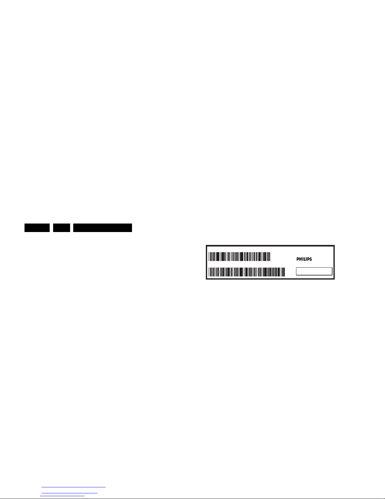
Identification: The bottom line of a type plate gives a 14-digit
serial number. Digits 1 and 2 refer to the production center (e.g.
AG is Bruges), digit 3 refers to the B.O.M. code, digit 4 refers
to the Service version change code, digits 5 and 6 refer to the
production year, and digits 7 and 8 refer to production week (in
example below it is 2006 week 17). The 6 last digits contain the
serial number.
Figure 2-1 Serial number (example)
2.3.6 Board Level Repair (BLR) or Component Level Repair
(CLR)
If a board is defective, consult your repair procedure to decide
if the board has to be exchanged or if it should be repaired on
component level.
If your repair procedure says the board should be exchanged
completely, do not solder on the defective board. Otherwise, it
cannot be returned to the O.E.M. supplier for back charging!
2.3.7 Practical Service Precautions
• It makes sense to avoid exposure to electrical shock.
While some sources are expected to have a possible
dangerous impact, others of quite high potential are of
limited current and are sometimes held in less regard.
• Always respect voltages. While some may not be
dangerous in themselves, they can cause unexpected
reactions that are best avoided. Before reaching into a
powered TV set, it is best to test the high voltage insulation.
It is easy to do, and is a good service precaution.
3. Directions for Use
You can download this information from the following websites:
http://www.philips.com/support
http://www.p4c.philips.com
E_06532_024.eps
260308
MODEL :
PROD.NO:
~
S
32PF9968/10
MADE IN BELGIUM
220-240V 50/60Hz
128W
AG 1A0617 000001
VHF+S+H+UHF
BJ3.0E LA
Mechanical Instructions
EN 7LC4.31E AA 4.
4. Mechanical Instructions
Index of this chapter:
4.1 Cable Dressing
4.2 Service Position
4.3 Assy/Panel Removal
4.4 Set Re-assembly
Notes:
• Figures below can deviate slightly from the actual situation,
due to the different set executions.
• Follow the disassembling instructions in described order.
4.1 Cable Dressing
G_16210_073.eps
190106

Mechanical Instructions
EN 8 LC4.31E AA4.
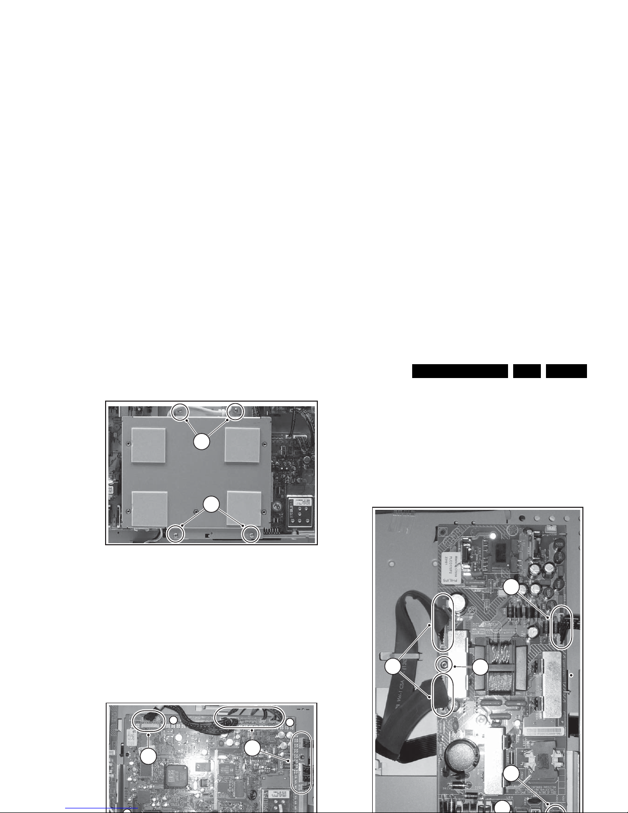
4.3.2 Side I/O Panel
Figure 4-3 Side I/O panel
1. Disconnect the cable [1] from the panel.
2. Release the two fixation clamps [2] and lift the panel out of
the bracket.
4.3.3 LED Panel
4.3.4 Keyboard Control Panel
Figure 4-5 Keyboard control panel
G_16210_074.eps
190106
2
2
1
2
1
G_16210_076.eps
190106
1
1
4
3
3
3
2
2
Mechanical Instructions
EN 9LC4.31E AA 4.
Figure 4-7 SSB cover shield
1. Release the cable from the plastic cable clip [1] on the
shield (see Figure “Cable clip on cover shield” above).
2. Remove the four fixation screws (2, see Figure “SSB cover
shield”; the screws are also indicated by arrows on the
shield) and remove the shield.
Notice that on one side, the shield is not only held by two
screws, but also by two brackets (see Figure “Cable clip on
cover shield” above).
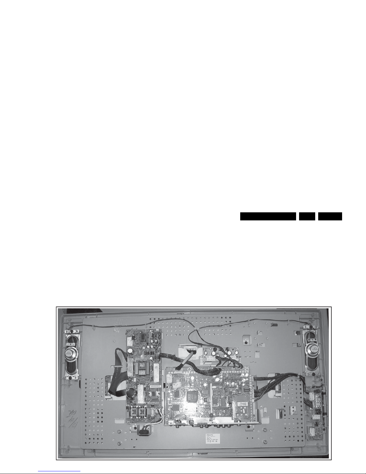
4.3.6 Small Signal Board
1. Very cautiously disconnect the LVDS cable [1] from the
panel (see Figure “SSB connectors”). Notice that this cable
is very fragile.
2. Disconnect the other cables [2] from the panel.
3. Remove the fixation screws [3] that secure the SSB
(depending on model) and also the fixation screws [4] from
the connector plate (see Figure “Connector screws”).
4. Take the panel out of its brackets.
4.3.7 Power Supply Panel (various models used)
F_15270_045.eps
190505
2
2
2
3
3
1
2
1
1
1
2
Mechanical Instructions
EN 10 LC4.31E AA4.
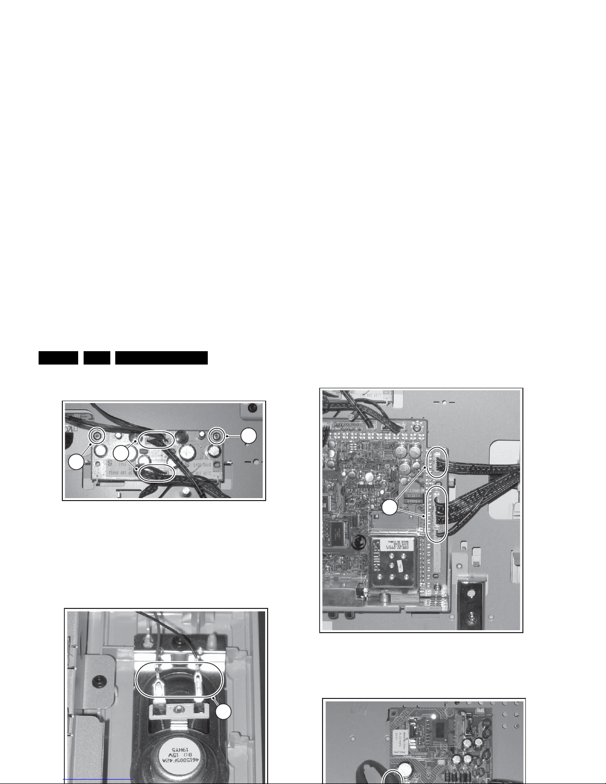
4.3.8 Audio Amplifier Panel
Figure 4-11 Audio amplifier panel
1. Disconnect all cables [1] from the panel.
2. Remove the fixation screws [2] from the panel.
3. Remove the panel.
4.3.9 LCD Panel
Figure 4-14 SSB connectors for side I/O, side control panel, and
LED
G_16210_080.eps
200106
2
2
1
1
G_16210_083.eps
200106
3
Mechanical Instructions
EN 11LC4.31E AA 4.
Figure 4-16 Shield screws of the LCD panel
Figure 4-17 LCD panel
To remove the LCD-panel, carry out the following steps:
1. Disconnect the cables [1] from the “L” and the “R”
loudspeakers (see Figure “Loudspeaker cables”).
2. Important: Unplug the LVDS connector [2] on the LCD
panel (see Figure “LVDS connector”), or better: remove the
cable completely.
Be careful, as this is a very fragile connector/cable!
• 32PF5411/10
• 32PF5521D/10
• 32PF5521D/12
• 32PF7321/12
• 32PF7321D/37
• 32PF7411/10
• 32PF7421D/37
• 32PF7521D/10
• 32PF7521D/12
• 42HF7544D/27
• 42PF7421D/37
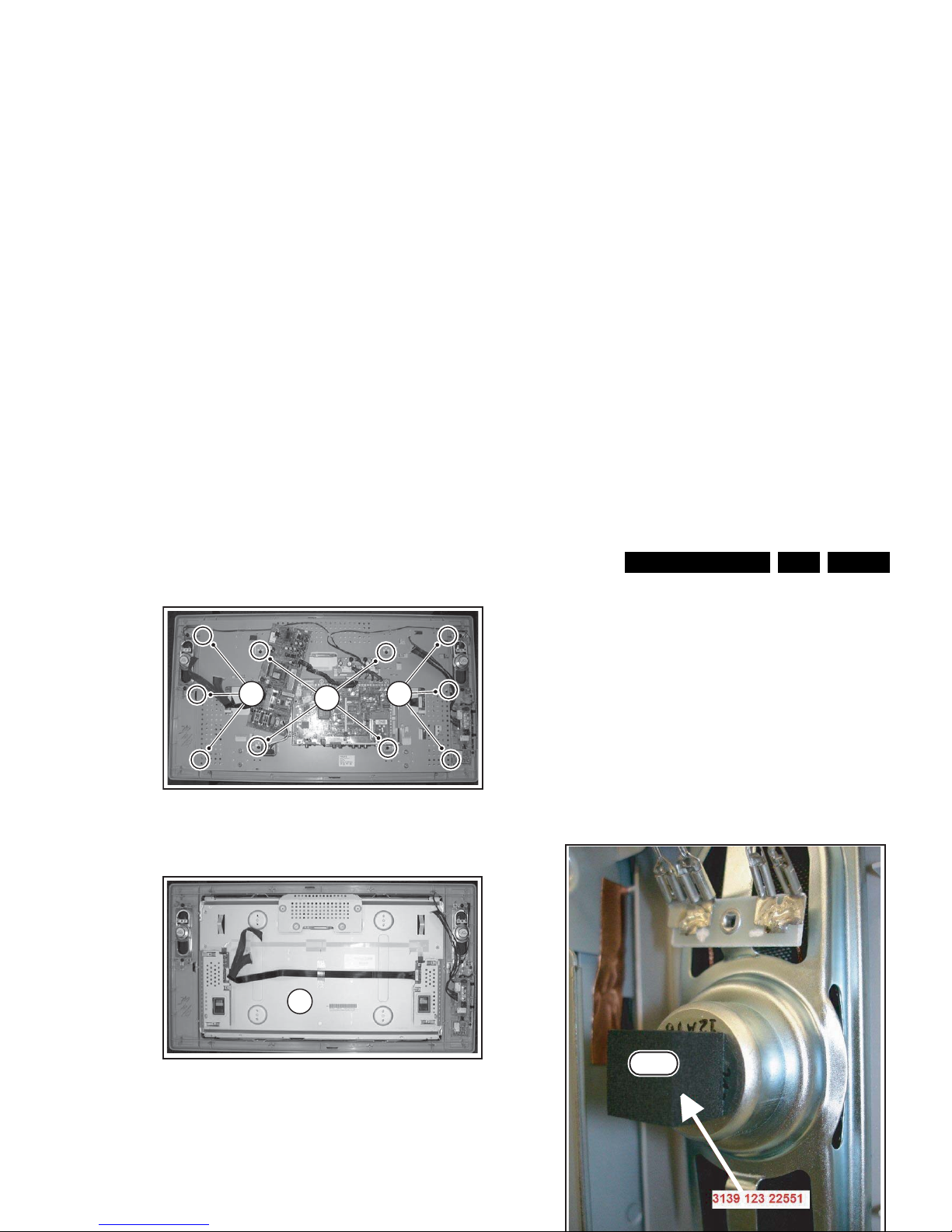
When a speaker of a set mentioned above is defective, you
need to order the speaker foam as well (12NC:
313912322551). It is required to prevent a rattling sound. Place
it on the speaker as shown by the photo below.
G_16210_085.eps
200106
7
6
6
G_16210_086.eps
200106
8
Foam
Service Modes, Error Codes, and Fault Finding
EN 12 LC4.31E AA5.
5. Service Modes, Error Codes, and Fault Finding
Index of this chapter:
5.1 Test Points
5.2 Service Modes
5.3 Problems and Solving Tips Related to CSM
5.4 Service Tools
5.5 Error Codes
5.6 The Blinking LED Procedure
5.7 Fault Finding and Repair Tips
5.1 Test Points
This chassis is equipped with test points. In the schematics,
test points are indicated with a rectangle box around Fxxx or
Ixxx, in the layouts with a half-moon.
Perform measurements under the following conditions:
• Television set in Service Default Mode.
• Video input: Colour bar signal.
• Audio input: 3 kHz left channel, 1 kHz right channel.
5.2 Service Modes
Service Default mode (SDM) and Service Alignment Mode
(SAM) offer several features for the service technician, while
the Customer Service Mode (CSM) is used for communication
between the call centre and the customer.
This chassis also offers the option of using ComPair, a
hardware interface between a computer and the TV chassis. It
offers the possibilities of structured troubleshooting, error code
reading, and software version read-out for all chassis.
Minimum requirements for ComPair: a Pentium processor, a
Windows OS, and a CD-ROM drive (see also paragraph
“ComPair”).
5.2.1 Service Default Mode (SDM)
Purpose
• To create a predefined setting for measurements to be
How to Enter
To enter SDM, use one of the following methods:
• Press the following key sequence on the remote control
transmitter: “062596” directly followed by the MENU button
(do not allow the display to time out between entries while
keying the sequence).
• Short one of the “Service” jumpers on the TV board during
cold start and apply mains (see Figures “Service jumper”).
Then press the mains button (remove the short after startup).
Caution: Entering SDM by shorting “Service” jumpers will
override the +8V-protection. Do this only for a short period.
When doing this, the service-technician must know exactly
what he is doing, as it could damage the television set.
• Or via ComPair.
Figure 5-1 Service jumper (component side)
G_16210_087.eps
200106
SDM
Service Modes, Error Codes, and Fault Finding
EN 13LC4.31E AA 5.
Figure 5-3 SDM menu
How to Navigate
Use one of the following methods:
• When you press the MENU button on the remote control,
the set will switch on the normal user menu in the SDM
mode.
• On the TV, press and hold the VOLUME DOWN and press
the CHANNEL DOWN for a few seconds, to switch from
SDM to SAM and reverse; or press the following key
sequence on the remote control transmitter: “062596”
directly followed by the OSD button to switch to SAM (do
not allow the display to time out between entries while
keying the sequence).
How to Exit
Switch the set to STANDBY by pressing the mains button on
the remote control transmitter or the television set.
If you turn the television set off by removing the mains (i.e.,
After entering SAM, the following screen is visible, with SAM in
the upper right corner of the screen to indicate that the
television is in Service Alignment Mode.
Figure 5-4 SAM menu
Menu Explanation
1. LLLLL. This represents the run timer. The run timer counts
normal operation hours, but does not count standby hours.
2. AAABCD X.YY. This is the software identification of the
main microprocessor:
– A= the project name (LC04.x).
– B= the region: E= Europe, A= Asia Pacific, U= NAFTA,
L= LATAM.
– C= the software diversity:
• Europe: T= 1 page TXT, F= Full TXT, V= Voice
control.
• LATAM and NAFTA: N= Stereo non-dBx, S=
Stereo dBx.
• Asian Pacific: T= TXT, N= non-TXT, C= NTSC.
00035 HSD21E1 1.00/S21LXN 1.00 SDM
ERR 0 0 0 0 0
OP 152 167 015 081 252 127 019
G_16210_089.eps
200106
G_16210_090.ep
s
110706
00035 HSD21E1 1.00/S21LXN 1.00 SAM
ERR 0 0 0 0 0
OP 152 167 015 081 252 127 019
. Clear Clear ?
. Options
. Tuner
. White Tone
. Audio
. NVM Editor
. SC NVM Editor
. Test Pattern
. ComPair Mode On

Service Modes, Error Codes, and Fault Finding
EN 14 LC4.31E AA5.
12. NVM Editor. Can be used to change the NVM data in the
television set. See table “NVM data” further on.
13. SC NVM Editor. Can be used to edit Scaler NVM.
14. ComPaIr. Can be used to switch on the television to In
System Programming (ISP) mode, for software uploading
via ComPair.
Caution: When this mode is selected without ComPair
connected, the TV will be blocked. Remove the AC power
to reset the TV.
How to Navigate
• In SAM, select menu items with the MENU UP/DOWN keys
on the remote control transmitter. The selected item will be
indicated. When not all menu items fit on the screen, use
the MENU UP/DOWN keys to display the next / previous
menu items.
• With the MENU LEFT/RIGHT keys, it is possible to:
– Activate the selected menu item.
– Change the value of the selected menu item.
– Activate the selected submenu.
• In SAM, when you press the MENU button twice, the set
will switch to the normal user menus (with the SAM mode
still active in the background). To return to the SAM menu
press the MENU button.
• When you press the MENU key in while in a submenu, you
will return to the previous menu.
• On the TV, press and hold the VOLUME DOWN and press
the CHANNEL DOWN for a few seconds, to switch from
SAM to SDM and reverse; or press the following key
sequence on the remote control transmitter: “062596”
directly followed by the MENU button to switch to SDM (do
not allow the display to time out between entries while
keying the sequence).
How to Store SAM Settings
To store the settings changed in SAM mode, leave the top level
SAM menu by using the POWER button on the remote control
transmitter or the television set.
How to Exit
Switch the set to STANDBY by pressing the mains button on
the remote control transmitter or the television set.
If you turn the television set “off” by removing the mains (i.e.,
Figure 5-5 CSM menu
Menu Explanation
1. Indication of the decimal value of the operation hours
counter, Main/Scaler software version (see “Service
Alignment Mode” for an explanation), and the service mode
(CSM = Customer Service Mode).
2. Displays the last five errors detected in the error code
buffer.
3. Displays the option bytes.
4. Displays the type number version of the set.
5. aaaaaa / b.ccc Firmware identification of the Pacific 3 and
the OTC:
– aaaaaa = the firmware version of the Pacific 3 (Pixel+)
– b.ccc = the firmware version of the OTC (for the 1000
page TXT decoder).
6. Indicates the television is receiving an “IDENT” signal on
the selected source. If no “IDENT” signal is detected, the
display will read “NOT TUNED”.
7. Displays the detected Colour system (e.g. PAL/NTSC).
1 00035 HSD21E1 1.00/S21LXN 1.00 CSM
2 CODES 0 0 0 0 0
3 OP 152 167 015 081 252 127 019
4 26PF5321/10
5 AAAAAA/B.CC
6 NOT TUNED
7 PAL
8 STEREO
9 CO 50 CL 50 BR 50
0 AVL Off
G_16210_091.eps
200106

Service Modes, Error Codes, and Fault Finding
EN 15LC4.31E AA 5.
Then:
1. Press the SMART PICTURE button on the remote control
transmitter repeatedly (if necessary) to choose
PERSONAL picture mode.
2. Press the MENU button on the remote control transmitter.
This brings up the normal user menu.
3. In the normal user menu, use the MENU UP/DOWN keys
to select the PICTURE sub menu.
4. Press the MENU LEFT/RIGHT keys to enter the PICTURE
sub menu.
5. Use the MENU UP/DOWN keys (if necessary) to select
BRIGHTNESS.
6. Press the MENU LEFT/RIGHT keys to increase or
decrease the value of the selected parameter.
7. Use the MENU UP/DOWN keys to select STORE.
8. Press the MENU RIGHT key to store the new value.
9. Press the MENU key to exit the PERSONAL picture mode.
White Line around Picture Elements and Text
If:
The picture improves after you have pressed the SMART
PICTURE button on the remote control transmitter,
Then:
1. Press the SMART PICTURE button on the remote control
transmitter repeatedly (if necessary) to choose
PERSONAL picture mode.
2. Press the MENU button on the remote control transmitter.
This brings up the normal user menu.
3. In the normal user menu, use the MENU UP/DOWN keys
to select the PICTURE sub menu.
4. Press the MENU LEFT/RIGHT keys to enter the PICTURE
sub menu.
5. Use the MENU UP/DOWN keys (if necessary) to select
SHARPNESS.
6. Press the MENU LEFT/RIGHT keys to increase or
decrease the value of the selected parameter.
7. Use the MENU UP/DOWN keys to select STORE.
8. Press the MENU RIGHT key to store the new value.
9. Press the MENU key to exit the PERSONAL picture mode.
Snowy Picture
8. Press the MENU RIGHT key to store the new value.
9. Press the MENU key to exit the PERSONAL picture mode.
5.4 Service Tools
5.4.1 ComPair
Introduction
ComPair (Computer Aided Repair) is a Service tool for Philips
Consumer Electronics products. and offers the following:
1. ComPair helps you to quickly get an understanding on how
to repair the chassis in a short and effective way.
2. ComPair allows very detailed diagnostics and is therefore
capable of accurately indicating problem areas. You do not
have to know anything about I
2
C or UART commands
yourself, because ComPair takes care of this.
3. ComPair speeds up the repair time since it can
automatically communicate with the chassis (when the μP
is working) and all repair information is directly available.
4. ComPair features TV software upgrade possibilities.
Specifications
ComPair consists of a Windows based fault finding program
and an interface box between PC and the (defective) product.
The (new) ComPair II interface box is connected to the PC via
an USB cable. For the TV chassis, the ComPair interface box
and the TV communicate via a bi-directional cable via the
service connector(s).
How to Connect
This is described in the ComPair chassis fault finding database.
TO
UART SERVICE
CONNECTOR
TO
UART SERVICE
CONNECTOR
TO
I2C SERVICE
CONNECTOR
TO TV
PC
RC out
RC in
Optional
Switch
Power ModeLink/
Activity
I
2
C
ComPair II
Multi
function
RS232 /UART

Service Modes, Error Codes, and Fault Finding
EN 16 LC4.31E AA5.
•ComPair I2C interface cable (3.5 mm Jack-to-SVHS plug):
9965 100 07325 (to be used with chassis LC7.5).
Note: For I
2
C it is compulsory to use this particular cable.
• ComPair UART interface cable (3.5 mm Jack-to-Jack):
3138 188 75051 (to be used with chassis LC7.5).
Note: For UART it is also allowed to use a standard “Jackto-Jack” cable.
Note: If you encounter any problems, contact your local
support desk.
5.4.2 LVDS Tool
Support of the LVDS Tool has been discontinued.
5.4.3 ComPair
Introduction
ComPair (Computer Aided Repair) is a Service tool for Philips
Consumer Electronics products. and offers the following:
1. ComPair helps you to quickly get an understanding on how
to repair the chassis in a short and effective way.
2. ComPair allows very detailed diagnostics and is therefore
capable of accurately indicating problem areas. You do not
have to know anything about I
2
C or UART commands
yourself, because ComPair takes care of this.
3. ComPair speeds up the repair time since it can
automatically communicate with the chassis (when the μP
is working) and all repair information is directly available.
4. ComPair features TV software upgrade possibilities.
Specifications
ComPair consists of a Windows based fault finding program
and an interface box between PC and the (defective) product.
The (new) ComPair II interface box is connected to the PC via
an USB cable. For the TV chassis, the ComPair interface box
and the TV communicate via a bi-directional cable via the
service connector(s).
How to Connect
This is described in the ComPair chassis fault finding database.
•ComPair I
2
C interface cable: 9965 100 09269.
Note: If you encounter any problems, contact your local
support desk.
5.5 Error Codes
The error code buffer contains all errors detected since the last
time the buffer was erased. The buffer is written from left to
right. When an error occurs that is not yet in the error code
buffer, it is displayed at the left side and all other errors shift one
position to the right.
5.5.1 How to Read the Error Buffer
You can read the error buffer in 3 ways:
• On screen via the SAM (if you have a picture).
Examples:
– ERROR: 0 0 0 0 0: No errors detected
– ERROR: 6 0 0 0 0: Error code 6 is the last and only
detected error
– ERROR: 9 6 0 0 0: Error code 6 was detected first and
error code 9 is the last detected (newest) error
• Via the blinking LED procedure (when you have no
picture). See “The Blinking LED Procedure”.
•Via ComPair.
5.5.2 How to Clear the Error Buffer
The error code buffer is cleared in the following cases:
• By using the CLEAR command in the SAM menu:
– To enter SAM, press the following key sequence on the
remote control transmitter: “062596” directly followed
by the OSD/i+ button (do not allow the display to time
out between entries while keying the sequence).
– Make sure the menu item CLEAR is selected. Use the
MENU UP/DOWN buttons, if necessary.
– Press the MENU RIGHT button to clear the error
buffer. The text on the right side of the “CLEAR” line will
change from “CLEAR?” to “CLEARED”
• If the contents of the error buffer have not changed for 50
hours, the error buffer resets automatically.
TO TV
Service Modes, Error Codes, and Fault Finding
EN 17LC4.31E AA 5.
Table 5-1 Error code overview
Example of error buffer: 129600
After entering SDM, the following occurs:
• 1 long blink of 5 seconds to start the sequence,
• 12 short blinks followed by a pause of 1.5 seconds,
• 9 short blinks followed by a pause of 1.5 seconds,
• 6 short blinks followed by a pause of 1.5 seconds,
• 1 long blink of 1.5 seconds to finish the sequence,
• The sequence starts again with 12 short blinks.
5.7 Fault Finding and Repair Tips
Notes:
• It is assumed that the components are mounted correctly
with correct values and no bad solder joints.
• Before any fault finding actions, check if the correct options
are set.
5.7.1 NVM Editor
In some cases, it can be handy if one directly can change the
NVM contents. This can be done with the “NVM Editor” in SAM
mode. With this option, single bytes can be changed.
Caution:
• Do not change the NVM settings without
understanding the function of each setting, because
incorrect NVM settings may seriously hamper the
correct functioning of the TV set!
• Do not change the Scaler NVM settings, as this will
hamper the DVI / HDMI functionality of the TV set!
• Always note down the existing NVM settings, before
changing the settings. This will enable you to return to the
original settings, if the new settings turn out to be incorrect.
Table 5-2 NVM editor overview
Error Error Description Check Item Diagram
0No Error
1 Mis-match of TV (Hercules)
SW and Scaler SW
Software
versions
N.A.
2 +12V from PSU error PSU A
3Plasma I
2
C error (only for
plasma sets)
N.A. N.A.
4I
2
C error while
communicating with the
Genesis Scaler
7801 B7 + B8
5 +5V protection 7752 B6
6 General I
2
C error;
communication between
ADC, analogue tuner, and/or
Columbus I
2
C failed
1102, 7L01,
7M00
B1 + B18
+ B19
7I
2
C error while
communicating with ADC
7L01 B18
8I
2
C error while
communicating with the
Scaler EEPROM
7C01 B11
9I
2
C error while
communicating with the
Hercules EEPROM (NVM for
TV).
Remark: when the Hercules
EEPROM is defective, the
Hercules should operate with
its default values.
7207 B2
10 I
2
C error while
communicating with the PLL
tuner
1102 B1
11 I
2
C error while
communicating with the 3D
combfilter IC-7M00
(Columbus)
7M00 B19
12 I
2
C error while
communicating with iBoard
μP (only iTV sets)
N.A. N.A.
2
Hex Dec Description
.ADR 0x000A 10 Existing value
.VAL 0x0000 0 New value
.Store Store?
Service Modes, Error Codes, and Fault Finding
EN 18 LC4.31E AA5.
Table 5-3 NVM Default values (option bit settings through NVM Editor in SAM Mode)
Byte Nr. Bit Feature/Mode Description
26PF5321/10/12
32PF5321/10/12
37PF5321/10/12
26PF7321/12
32PF7321/12
37PF7321/10/12
42PF5421/10
Byte 0
174(dec)
0 QSS (LSB) Mode of quasi split sound amplifier 1
1 FMI Connection of output of QSS amplifier 1
2 HCO EHT tracking mode 0
3 HP2 Synchronization of OSD/Text display 1
4 FSL Forced slicing level for vertical sync 1
5 TFR DC transfer ratio of luminance signal 1
6 OSVE Black current measuring in overscan 0
7 MVK (MSB) (For Future Usage, as defined by software) 0
Total Dec Values 59
Total Hex Values 3B
Byte 1
175(dec)
0 PSE PSE 0
1OPC OPC 0
2PRIS PRIS 0
3 CONTINUOUS FACTORY Continuous factory mode 1
4 WHITE PATTERN ON Last colour pattern status in factory mode 0
5 SDM MODE Service default mode on/off 0
6 SAM MODE Service Align mode on/off 0
7 SVMA Scavem On / Off 0
Total Dec Values 8
Total Hex Values 08
Byte 2
176(dec)
0 MUTE STATUS Mute status 0
1 TUNER AUTO MODE Auto mode 1
2 CABLE MODE Cable/Antenna mode 0
3 LAST POWER MODE Last power status of the set 1
4 CHILD LOCK MODE Child lock enabled 0
5 SURF MODE Surf mode on/off 0
6 FACTORY MODE Factory mode on 1
7 PSNS For PAL colour enhancement in ES4 1
Total Dec Values 202
Total Hex Values CA
Byte 3
177(dec)
0 RADIO/TV MODE Radio mode or TV mode 0
1 WAKE-UP MODE WAKE-UP MODE 0
2 HOTEL MODE TV in Hotel mode 0
3 HOTEL KBD LOCK Keyboard locked 0
4HBL HBL 0
5 BLS Blue stretch mode 1
6SL SL 0
Service Modes, Error Codes, and Fault Finding
EN 19LC4.31E AA 5.
5.7.2 Load Default NVM Values
In case a blank NVM is placed or when the NVM content is
corrupted, default values can be downloaded into the NVM.
(For empty NVM replacement, short the SDM with a jumper
and apply the mains voltage. Remember to remove the jumper
after the reload is completed). After the default values are
downloaded, it will be possible to start up and to start aligning
the TV set. This is no longer initiated automatically; to initiate
the download the following action has to be performed:
1. Switch “off” the TV set by disconnecting the AC Power
plug.
2. Short circuit an SDM jumper (keep short-circuited).
3. Press P+ or Ch+ on the local keyboard (and keep it
pressed).
4. Switch on the TV set via the AC Power plug.
5. Keep pressing the P+/Ch+ button until the set has started
5. Manually store a known channel and check if there is IF
output at Tuner pin 11.
6. Check the tuning DC voltage at pin 2 of the Tuner. The DC
voltage should vary according to the frequency/channel
being chosen.
7. If the tuning voltage is OK, check the tuner output, pin 11.
8. If it has no output, the Tuner may have a defect. Change
the Tuner.
Sound in Picture Problem for L' System (rolling horizontal
lines)
1. Check whether AGC L' in SAM mode is set to 0.
2. If yes, align the set to correct value.
Required System is not Selected Correctly
Check whether a Service jumper (#4204 & 4205, 0805 size) is
present. If yes, remove it.
Byte 6
180(dec)
0 LTI status LTI last status 0
1 Inc_Life_Time Inc_Life_Time 0
2 PC_Mode PC_Mode 0
3 HD_Mode HD_Mode 0
4 Tact_Switch Tact_Switch 0
5 Set_In_Special_Stby Set_In_Special_Stby 0
6 Hotel_OSDDisplay Hotel_OSDDisplay 0
7 Hotel_MonitorOut Hotel_MonitorOut 0
Total Dec Values 0
Total Hex Values 00
Byte 7
181(dec)
0 Hotel_IconMode Hotel_IconMode 0
1DBE DBE 1
2SD SD 0
3 Set_in_PC_Sleep_Mode Set_in_PC_Sleep_Mode 0
4 Reserved Reserved 1
5 Reserved Reserved 0
6 Reserved Reserved 0
7 Reserved Reserved 0
Total Dec Values 18
Total Hex Values 12
Byte Nr. Bit Feature/Mode Description
26PF5321/10/12
32PF5321/10/12
37PF5321/10/12
26PF7321/12
32PF7321/12
37PF7321/10/12
42PF5421/10

Service Modes, Error Codes, and Fault Finding
EN 20 LC4.31E AA5.
input of the scaler) is only used for teletext. This means that no
mixed mode (video plus teletext simultaneously) is possible. If
there is sound and teletext, but no video and user menu (blank
screen), the digital path (Hercules - ADC - Columbus - Scaler)
is faulty. If there is sound but no teletext, the back-end part
(Scaler - LCD panel) is faulty. In Crystal Clear models, which
do not have an ADC and Columbus, the RGB path (analogue
input of scaler) is used for both video and teletext.
No TV, but PC is Present
1. Check if Hsync_SDTV and Vsync_SDTV are present at pin
1 & pin13 of 7E03.
2. If they are present, check teletext output.
3. If there is no teletext output, the IC TDA150xx may be
defect.
5.7.6 Power Supply
Check Fuse
The power supply (various models are used) contains one fuse
near the AC input connector X002.
1. Check with power supply in “off” state by means of ohmic
measurement.
2. Fuse X102 may open in case of severe lightning strikes
and/or failures in the power supply.
3. Check the standby signal at pin 10 of X200. ON is HIGH,
OFF is LOW. During standby mode only the 3,3 V is
present at pin 10.
Protections Concept on Power Supply Board (two models)
1. 12 V output (pin 8 of X200): Short-circuit protected by 2.5
A fuse X610. Over-voltage protection when output voltage
is more than 40% above nominal value.
2. Vaudio output (+18 or +24 V, depending on power
supply model used); (pin 1 of X200): Short-circuit proof
(+18 V version has 2.5 A fuse X660). Over voltage
protection when output voltage is more than 40% above
nominal value.
3. 3V3STBY output (pin 3 & 4 of X200): Short-circuit proof
with auto-restart. Over voltage protection when output
voltage is more than 40% above nominal value.
4. 24 V output (for inverter X520 & X530): Short-circuit
Block Diagrams, Test Point Overviews, and Waveforms
EN 21LC4.31E AA 6.
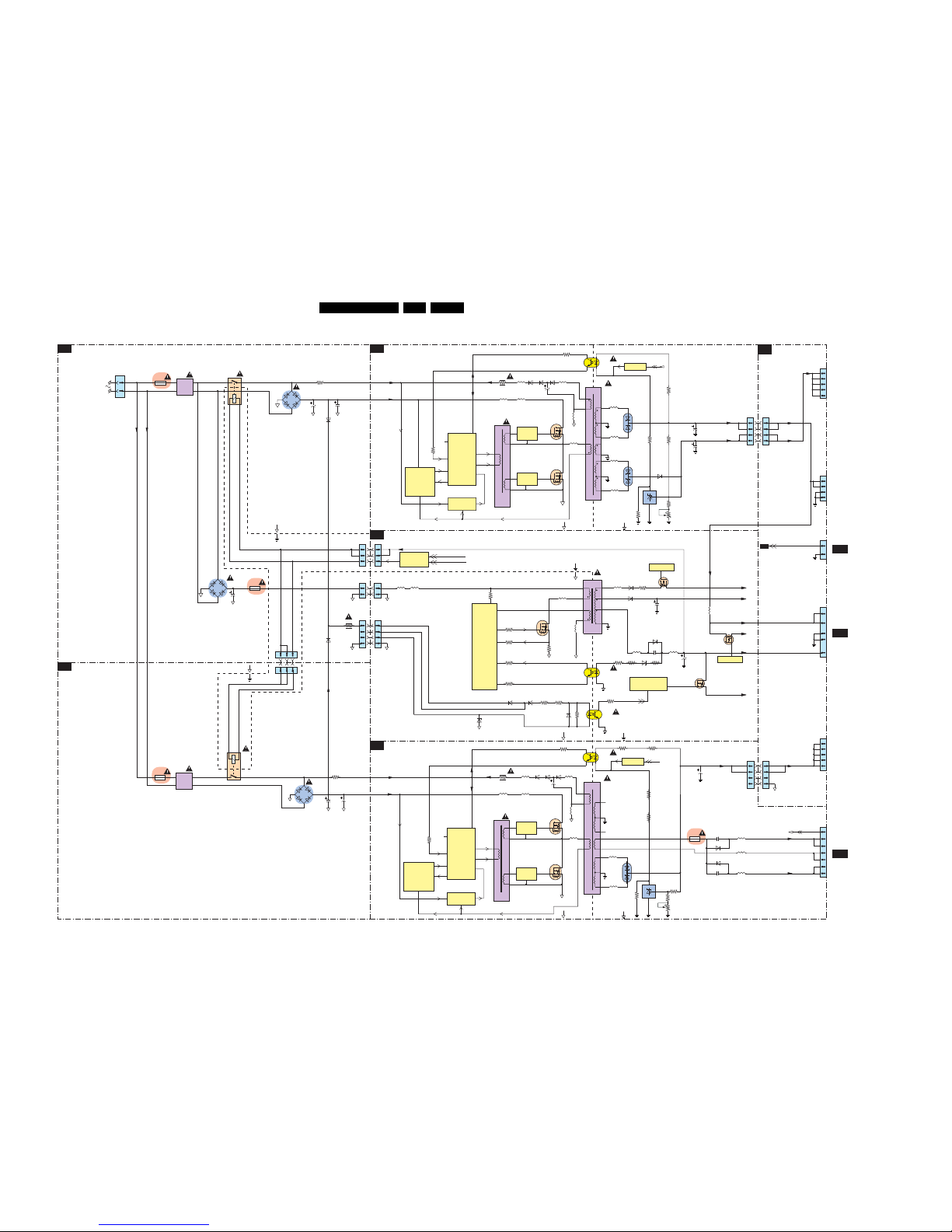
6. Block Diagrams, Test Point Overviews, and Waveforms
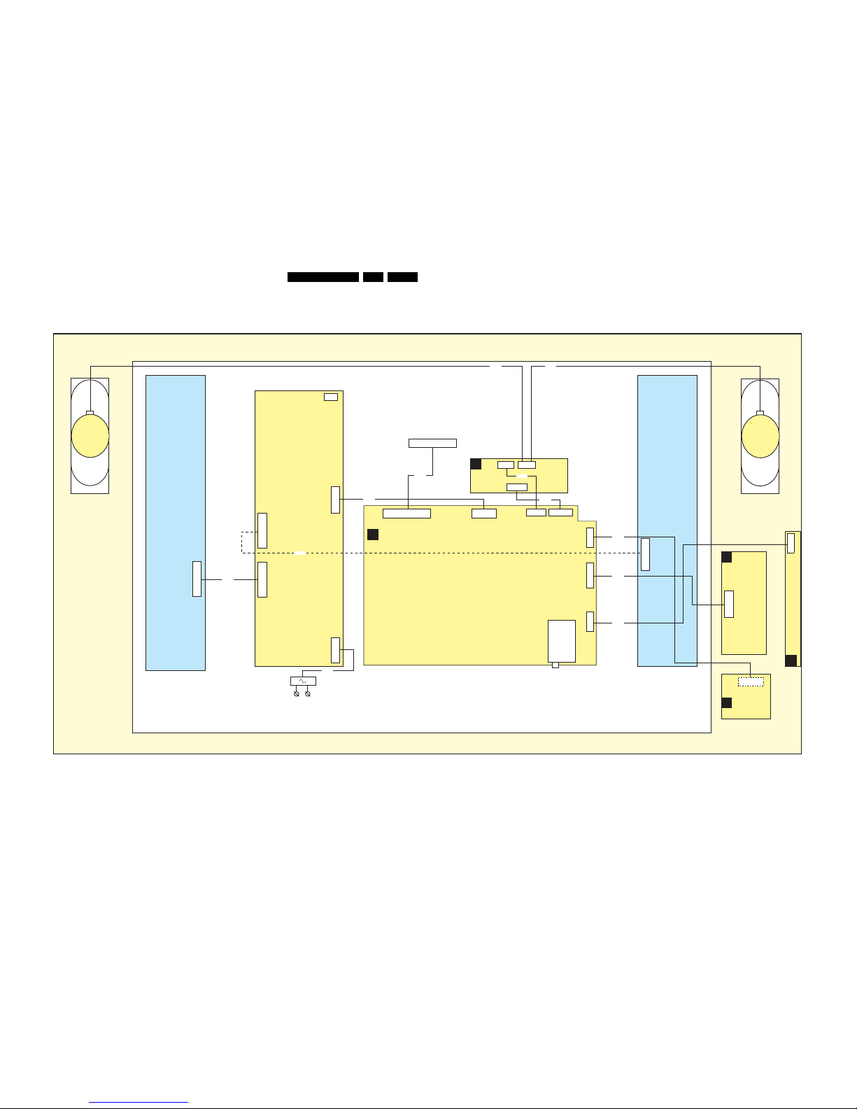
Wiring Diagram 26" & 32"
LEFT
SPEAKER
RIGHT
SPEAKER
12P
31P
G_16210_058.eps
010206
30P
12P
X200
12P
X530
1P06
1J02
POWER
IN
X002
B
SSB
D
SIDE AV
J
IR/LED/LIGHT
SENSOR
LVDS CONNECTION
TO DISPLAY
INVERTER
6P
1870
1304
(1M06)
POWER
SUPPLY
1001
1003
9P
1J04(1M52)
3P
1J03
1002
30P
8J02
3P
1684
6P
1K00(1M21)
12P
1K01(1M06)
3P
1K02
X220
14P
14P
X520
INVERTER
INVERTER
2P3
3P
9P
3P
4P
12P
AC POWER
INLET
TUNER
E
KEYBOARD CONTROL
C
CLASS D
AUDIO
AMPLIFIER
8J04
8J03
8K01
8002
8520
8870
8903
8903
8P06
8684
WIRING 26"- 32"
12P
8520
EN 22LC4.31E AA 6.
Block Diagrams, Test Point Overviews, and Waveforms
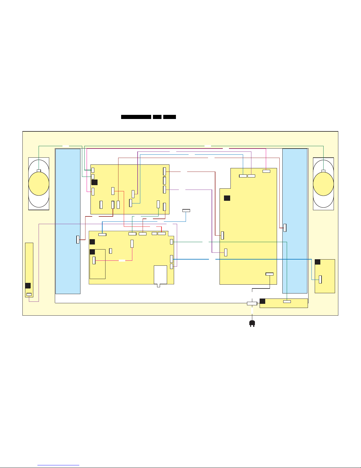
Wiring Diagram 37"
INVERTER
0345
6P
J
LED PANEL
LCD PANEL
RIGHT
SPEAKER
LEFT
SPEAKER
G_16210_059.eps
280606
WIRING 37"
INVERTER
14P
12P
1304
4P
1305
3P
1306
2P3
A
LCD SUPPLY
1M02
7P
1308
2P3
1309
3P
D
SIDE AV
1M36
11P
TUNER
B
SSB
1J04
9P
1N17
30P
1J03
3P
1K02
3P
1K04
11P
1K00
6P
1J01
11P
1442
14P
1J00
10P
1N20
3P
SA
STANDBY
1316
12P
1739
9P
1317
12P
1309
3P
1304
4P
1306
2P3
1307
4P
1305
3P
1M03
10P
1M46
11P
1736
3P
1735
3P
1M02
7P
1319
14P
LVD S
TO DISPLAY
8002
AC INLET
8187
(8188UK)
1M01
3P
E
KEYBOARD CONTROL
8902
8903
8305
8306
8521
8304
8309
8302
8J04
8337
8P06
8322
8870
8K01
8101
8520
T
OTCFLASH
1000
14P
8000
Block Diagrams, Test Point Overviews, and Waveforms
EN 23LC4.31E AA 6.
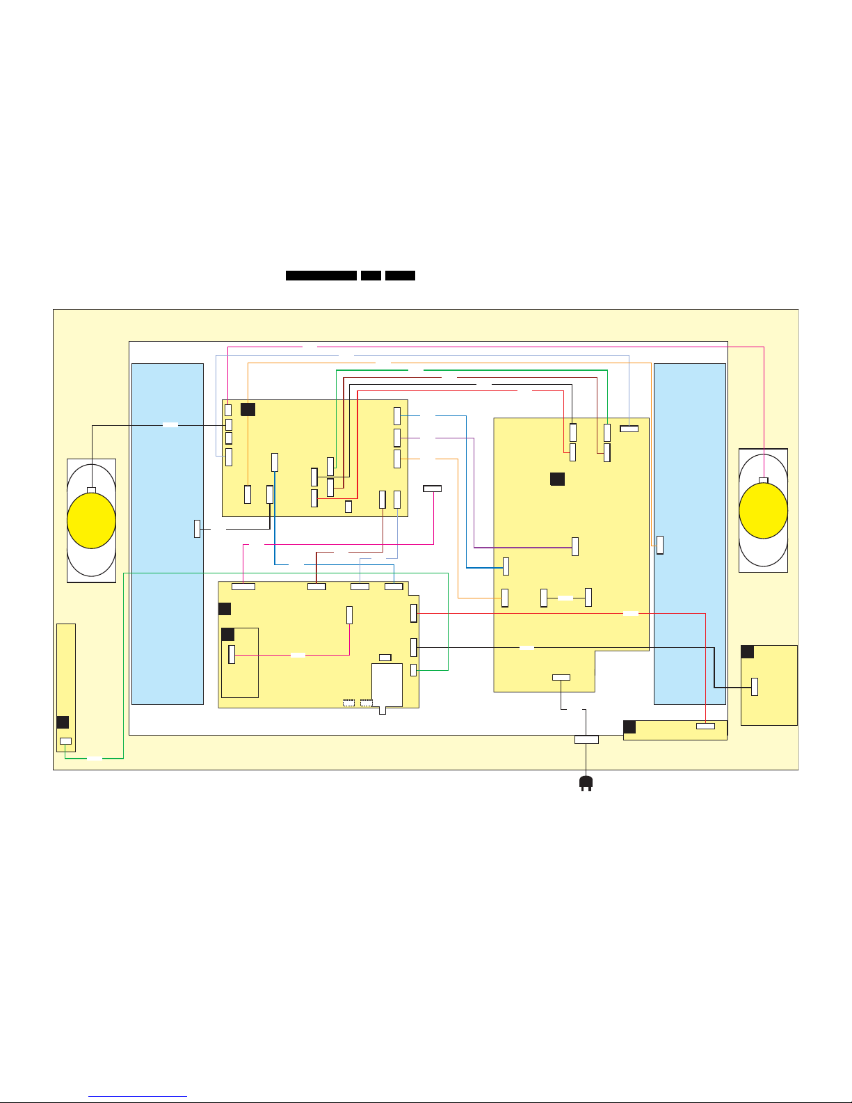
Wiring Diagram 42"
1J04(1M52)
9P
1N17
31P
1J01(1M46)
11P
Tuner
1177
3P
1K04(1M06)
11P
0345
6P
1M36
11P
1M01
3P
B
SSB
INVERTER
D
E
CONTROL BOARD
J
LED SWITCH
PANEL
LCD PANEL
AC INLET
RIGHT
SPEAKER
LEFT
SPEAKER
G_16210_101.eps
190506
1K02
3P
1303
4P
1320
3P
1B06
3P
12P
1736
2P3
1735
2P3
1738
2P3
1M02
7P
1316
12P
1739
9P
1319
14P
1320
3P
1303
4P
1306
2P3
1307
4P
1305
3P
1M03
10P
1M46
11P
1M10
4P
A
MF + SUPPLY
1M02
7P
1308
2P
30P
8302
8736
INVERTER
14P
SIDE I/O
8735
8319
8306
8305
8317
8304
8309
8136
8120
1K00(1M21)
6P
1J00(1M03)
10P
8146
8103
8152
1306
2P3
8150
8101
1103
3P
1151
3P
Compair
UART
SA
STANDBY / AUDIO
1304
4P
1309
3P
1307
4P
1305
3P
1C05
3P
1309
3P
1304
4P
8303
8320
8307
8308
1420
WIRING 42" LCD
1442
14P
T
OTCFLASH
1000
14P
8000
LVD S
EN 24LC4.31E AA 6.
Block Diagrams, Test Point Overviews, and Waveforms
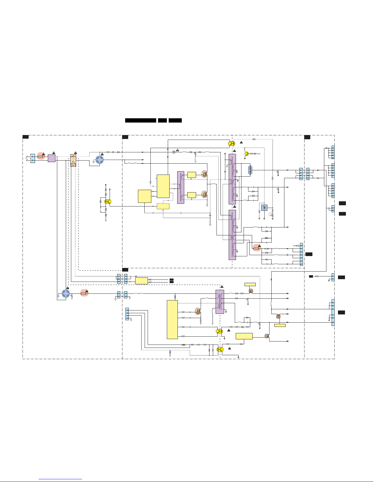
Block Diagram Supply 37"
CONNECTIONS
SA1
STANDBY
SA2
MAINS FILTER + STANDBY
A1
SUPPLY
A2
6307
GBJ6J
-
+
6306
DF06M
-
+
7001
MC34067P
15
7011
7012
7007
HIGH
SIDE
DRIVE
7004
7009
5001
BIAS SUPPLY
SOFT
START
+
CURRENT
PROTECTION
CONTROL
VCC
OSCC
ERROR
SOST
OB
OA
FI
2
4
11
7
11
14
12
10
6
7
5011
7008
LOW
SIDE
DRIVE
10
9
2003
60246025
3007
7010
TS2431
3030
1314
T5AH
1308
5305
5306
MAINS
FILTER
2
1
OVER
VOLTAGE
PROTECTION
400V_HOT
25V_HOT
HOT COLD
HOT
COLD
SUPPLY 37"
399V_HOT
5002
1007
T5A
VSND_POS
VSND_NEG
GND_SND
+24Vb
+24Va
+12V
400V_HOT
2303
2020
2022
2060
PRINTED
COMPONENT
HOT COLD
VREF
5
N.C.
5008
5007
25V_HOT
399V_HOT
6315
6316
6318
6317
RES
6314
6304
2319
3318
3000
2029
2045
6021
6041
5025
5026
+12V_A
+12V_+24V
HOT
COLD
CONTROL
3
STAND B Y
7100
7101
7105
VTUN
+11V
+8V6
+5V2
+5V_SW
5500
+12V
6
7
10
STANDBY
7507
7506
7512
STANDBY
OVERVOLTAGE
PROTECTION
8
B01B
TO 1M46
(1J01)
SSB
5
2
1
+5V2
STANDBY: LOW = ON
HIGH = STBY
CONTROL
7505/7509/7560
Prot-OVV
+12V_A
PROT-OVV
G_16210_060.eps
260906
TO
DISPLAY
1305
11
1305
22
33
1306
11
1306
22
1
1307
2
3
4
1304
44
1304
33
22
11
6504
6140
3509
5110
5507
5103
6107
6122
3158
PROT_AUDIOSUPPLY
2512
5506
2513
3128
3113
3124
2141
5504
5505
5104
5105
3108
3127
3104
3150
3101
3155
6151
6150
3156
6153
3157
6156
1
2
3
4
5
1316
1
2
1M10
1M03
7
1M46
4
7
3100
11
2
1
2
3
4
5
1317
1M02
7
6
4
5
3
2
1
TO 1M02
AUDIO
TO
DISPLAY
SA1
SA2
2009
6029
2021
6030
5020
5018
5019
2042
2049
6031
6040
5021
5022
DC_PROT
7003
3031
3052
3057
VS Voltage
Adj.
3026
3025
5017
5012
5009
2059
5010
DC_PROT
3V MAX
1V MAX STBY
7150
TCET1102
2143
7501
TCET1102
2143
7002
TCET1102
2143
7307
TCET1102
2143
B16
B01B
TO 1M03
(1J00)
SSB
B16
SA3
HOT COLD
6019
STPS20L40CFP
6019
STPS20L40CFP
7005
STP15NK50
7006
STP15NK50
7102
STP15NK50
7531
7131
7511
2
3
1
4
1350
9311
RES
RES
1
4
1315
T1A
9
SA2
1
2
3
4
5
1319
TO
DISPLAY
B01B
TO 1301
IBO ZAPPER
(ONLY DVB SETS)
K3
B01B
TO 1329
SIDE AV
D
Block Diagrams, Test Point Overviews, and Waveforms
EN 25LC4.31E AA 6.
Block Diagram Supply 42"
G_16210_102.eps
310708
SUPPLY PART A
A2
STANDBY
SA2
SUPPLY PART B
A4
CONNECTIONS
SA1
MAINS FILTER + STANDBY
PART B
A3
MAINS FILTER + STANDBY PART A
A1
SUPPLY 42"
6807
GBJ6J
-
+
7001
MC34067P
15
7017
7018
7007
7004
7009
5001
BIAS SUPPLY
SOFT
START
+
CURRENT
PROTECTION
CONTROL
VCC
OSCC
ERROR
SOST
OB
OA
FI
2
4
11
7
11
14
12
10
6
7
5
3
7
8
9
10
11
3
1
2
12
13
5002
7008
10
9
3007
7010
TL431ACD
VS Voltage
Adj.
+12V_A
+12V_+24V
5400
5401
5403
2
3
MAINS
FILTER
1
4
6506
DF06M
-
+
1450
OVER
VOLTAGE
PROTECTION
400V_HOT_A
25V_HOT_A
14
15
16
6021
STTH2003CFP
6H07
GBJ6J
-
+
7U01
MC34067P
15
7U17
7U18
7U07
HIGH
SIDE
DRIVE
7U04
7U09
5U01
BIAS SUPPLY
SOFT
START
+
CURRENT
PROTECTION
CONTROL
VCC
OSCC
ERROR
SOST
OB
OA
FI
2
4
11
7
11
14
12
10
6
7
5
3
7
8
9
10
11
12
13
5U02
7U08
LOW
SIDE
DRIVE
10
9
7U10
TL431ACD
VS Voltage
Adj.
+24V
5D00
5D01
5D03
2
3
MAINS
FILTER
1 4
1D50
OVER
VOLTAGE
PROTECTION
400V_HOT_B
25V_HOT_B
14
15
16
400V_HOT_B
VSND_POS
VSND_NEG
MAINS INPUT
CONTROL
3
7100
7101
7105
VTUN
+11V
+8V6
+5V2
+5V_SW
+12V
6
7
10
STANDBY
7507
7506
7512
STANDBY
OVERVOLTAGE
PROTECTION
8
5
2
1
+5V2
STANDBY: LOW = ON
HIGH = STBY
3V MAX
1V MAX STBY
2020
2022
CONTROL
7505/7509/7560/
Prot-OVV
+12V_A
DC_PROT
DC_PROT
DC_PROT
DC_PROT
PROT-OVV
VREF
5
TO
DISPLAY
TO
DISPLAY
+24V_2
VREF
5
5B92
2
1308
1
1400
3A15
1401
T1A
2503
6156
3810
2815
China
2816
6157
3406
2H15
China
2H16
1305
1 1
1305
2 2
3 3
1306
1 1
1306
2 2
1307
1 1
1307
2 2
3 3
4 4
1C05
1 1
1B06
2 2
3 3
3000
6080
6078
2003
3022
3052
3026
3030
1304
4 4
1304
3 3
2 2
1 1
3057
+12V
+24Va
7030
6014
3025
6504
6140
3509
5110
5507
5103
6107
6122
3158
PROT_AUDIOSUPPLY
2512
5506
2513
3128
3113
3124
2141
5504
5505
5104
5105
3108
3127
3150
3101
3155
6151
6150
3156
6153
3157
6156
3U07
3U57
6U78
6U79
2U03
2B91
2B93
6B91
6B93
5B93
5B91
1303
1 1
1303
2 2
3 3
4 4
3U30
3U26
3U24
3U22
2U22
1316
1
2
3
4
5
1M10
1
2
1M46
9
1
7
1319
(1317)
1
2
3
4
5
1M02
6
5
3
2
1
4
3U28
3U00
6U77
5U40
5U10 5U17
5U08
5U07
7
DC_PROT
3U25
6077
5010
5017
3028
5007
5008
5U09
5009
3U52
3U39
MAINS_L
MAINS_N
3H10
3100
11
2
1M03
7
4
SA3
3
4
1D00
3A15
6019
STPS20L40CFP
5027
5028
1
3
2
6021
STPS20L40CFP
5025
5026
7002
TCET1102
2
1 4
3
7005
STP15NK50
7006
STP15NK50
HIGH
SIDE
DRIVE
5040
LOW
SIDE
DRIVE
1
3
2
6021
STPS20L40CFP
5U25
5U26
1U07
T5A
7U05
STP15NK50
7U06
STP15NK50
7U02
TCET1102
2
1 4
3
7501
TCET1102
2
1 4
3
7150
TCET1102
2
1 4
3
7102
3104
5500
7131
7511
B01B
TO 1M46
SSB
N.C.
TO 1M02
AUDIO
B16
B01B
TO 1M03
SSB
B16
SA3
RES
HOT GROUND COLD GROUND
HOT GROUND
COLD GROUND
HOT GROUND COLD GROUND
HOT GROUND COLD GROUND
STANDBY
SA2
HOT GROUND
COLD GROUND
HOT GROUND
COLD GROUND
RES
7531
EN 26LC4.31E AA 6.
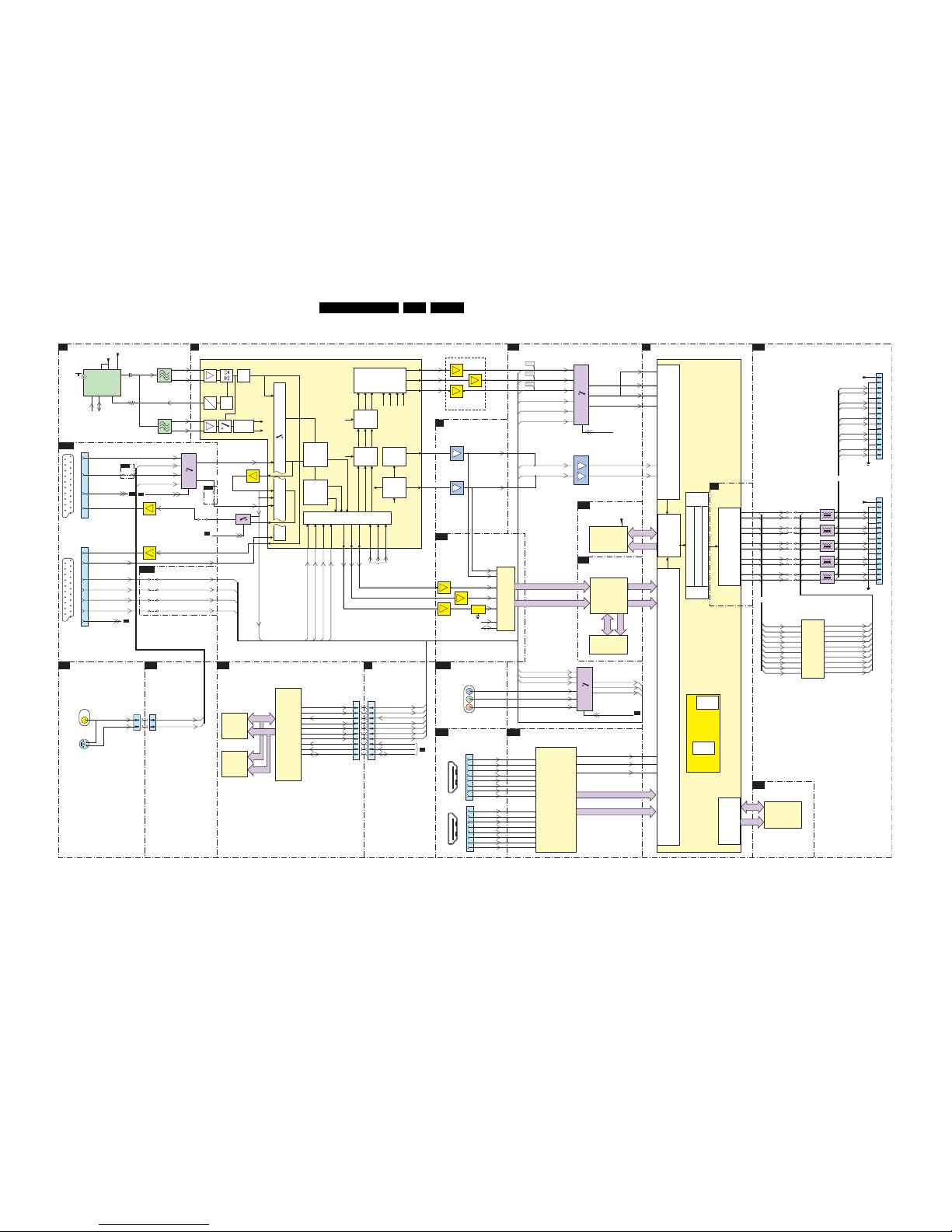
Block Diagrams, Test Point Overviews, and Waveforms
Block Diagram Video
B1
TUNER & VIF
B15A
SCART ANALOG IO
B2
HERCULES
B14
DIGITAL IO
B13
MUX-SYNC INTERFACE
B7
SCALER
B11
FLASH/CONTROL
B10
SDRAM
B3
SYNC INTERFACE
VIDEO
B18
ADC
B17
SIDE
CONNECTIONS
D
SIDE AV
B19
COLUMBUS
(Dig. PAL/NTC Comb)
B20
PACI FI C3
HERCULES
B15B
B15B
B12
HDMI
B15A
SCART ANALOG IO
T
OTC-FLASH
(FOR 1000pg TXT)
B3
SYNC INTERFACE
(TO OTC-FLASH)
B15B
DMMI
DD(0-15)
1152
UV1318S
RF
IN
TUNER
2156
11
1154
VIF1
VIF2
5
4
1
4
5
1
3154
RF_AGC
SCL
SDA
DC
AC
AGC
Detect
21
1
SCART 2
1G02
20
15
SC2_Y_IN
SC2_Y_IN_1
SC2_C_IN
1G01
20
7
8
16
15
11
SC1_CVBS
_IN
SC1_CVB
S_IN
21
1
SCART 1
24
25
31
51
52
55
SC2_CVBS_MON_OUT
19
SC1_CVBS_RF_OUT
43
EF
7G01
77 78 79 80
EF
7208
R_OTC_SDTV
EF
7209
G_OTC_SDTV
EF
7210
B_OTC_SDTV
85
86
87
74 75 76 70 71 72
22
67
7E01
SC1_R_CVI_Pr_IN
SC1_G_CVI_Y_IN
SC1_B_CVI_Pb_IN
27
3
7
25
1
5
R_PR+
G_Y+
B_PB+
17
14
11
Vsync_SDTV
Hsync_SDTV
AVSYNC
AHSYNC
7E04
5
1
8
4
L4
L3
ANALOG
INPUT
PORT
DVI/HDMI
INPUT
PORT
7B01
K4D263238F
SDRAM
1Mx32x4
FSDATA
FSADDR
7801
GM1501
GRAPHIC
ZOOM
DISPLAY
TIMING
GEN.
VIDEO
ZOOM
OSD CONTROLLER
OUT BLENDER
BRIGHTNESS/CONTRAST/HUE/SAT
EXTERNAL
ROM
INTERFACE
7C03
M29W400DT55N6E
FLASH
ROM
512Kx8
OCMDATA
OCMADDR
1N17
1
11
10
12
14
13
15
19
18
20
27
26
28
22
21
23
LVDS_VCC
TXB0-
TXB3+
TXB0+
TXB1-
TXB1+
TXBC+
TXBC-
TXB2-
TXB2+
TXB3-
RGB/Pr Pb Insert
YUV Interface
RGB Matrix
Blue & Black
Strech
Gamma Corr.
PAL/NTSC/
SECAM
Decoder &
Baseband
Delay
Sync Sep
H-OSC
H-Shift
H-Drive
Vertical &
East-West
Geometry
CVBS/Y
VDRB
H/V
HOUT
RO
GO
BO
INSSW3
Chroma
Yint
R/Pr-3
G/Y3
B/Pb-3
YOUT
VOUT
UOUT
VIN
UIN
YIN
B_OSD
G_OSD
R_OSD
Fast Blanking
Peaking
SCAVEM
U/V Delay
Skin Tone
U/V Tint
Saturation
YUV
YUV in/out
SAT
SCAVEM
on text
Dig. 2H/4H
Combfilter
Y Delay Adj.
c
cvbs/y
Sound
Traps
Video
Switch
+
Control
Uint
Vint
CVBS1
BINA|Pb
GINA|YINA
RINA|Pr
FRAME
STORE
CONTROL
MICRO
CONTROLLER
UART
INTERFACE
INTERNAL
RAM
QSS Mixer
AM Demod.
AM
QSS/FM
1156
4
5
1
SIF1
SIF2
29
30
FE00
FE01
FE02
IF-TER
AE16
AF11
AF16
AF12
AE15
AF15
AE12
AF13
AE14
AF14
D2
C2
B2
7217
TDA15021H
RO
GO
BO
Vsync_SDTV
Hsync_SDTV
INTF_Y_OUT
INTF_U_OUT
INTF_V_OUT
SC1_CV1_DMMI_B_P
b_IN
SC1_FBL_IN_1
SC1_CV1_DMMI_R_
Pr_IN
SC1_CV1_DMMI_G_Y_IN
19
STATUS
_2_IN|OUT
8
STATUS
_1
67
+5SW_a
+VTUN
7436-2
43
7436-1
21
N.C.
EF
7L61/7L62
EF
7L51/7L52
EF
7L71
7L01
P3563M-LF
A/D
CONV.
COL_Di(1-9)
COL_YA(1-9)
COL_A
COL_DQ
7M00
T6TU5XBG
COLUMBUS
DIGITAL COMB
FILTER
DRAM
512Kx16x2
7M01
MSM56V16
+2V5_DDR
95
G_16210_061.eps
260706
9
6
11
2
3
37
38
SCL
SDA
COL_Do(1-8)
COL_YB(1-8)
7E00
1
13
3
5
2
12
15
14
4
C3
SOG
2
1304
(1M36)
1K01
(1K04)
2
4
4
1
5
SVHS
2
4
3
1301
(1001)
1302
(1002)
EF
7206
64
58
7G11
2
9
12
15
14
FRONT
_Y_CVB
S_IN
1
FRONT_C_IN
13
59
SC2_AV3_C_IN
SC1_FB
L_IN
CVI_Pr_IN
CVI_Y_
IN
CVI_Pb_IN
SC1_FBL_IN_1
SC1_CV1_DMMI_R_Pr_IN
SC1_CV1_DMMI_G_Y_IN
SC1_CV1_DMMI_B_Pb_IN
B2
B2,B13
B2,B13
B2,B13
B15b
B15b
B15b
B15b
SC1_CV1_DMMI_R_Pr_IN
SC1_CV1_DMMI_G_Y_IN
SC1_CV1_DMMI_B_Pb_IN
B15b
B15b
B15b
SC1_R_CVI_Pr_IN
SC1_G_CVI_Y_IN
SC1_B_CVI_Pb_IN
B13
B13
B13
B13
B13
B13
B3
B3
EF
7G02
7219
48
13
12
14
4G18
4G31
4G14
4G15
4G17
4G16
B2
B2
FRONT_YCVBS_IN
FRONT_C_IN
CVB
S_COMB
B9
SCALER
LVDS
PACIFIC3
7N00
T6TF4AFG
TXB0-
TXB3+
TXB0+
TXB1TXB1+
TXBC+
TXBC-
TXB2TXB2+
TXB3-
OR
4N02
4N09
4N01
4N10
4N04
4N03
4N07
4N08
4N06
4N05
TXO0+
TXO0-
TXO1+
TXO1-
TXO2+
TXO2-
TXO3+
TXO3-
TXOC+
TXOC-
OR
LVDSA+
LVDSA-
LVDSB+
LVDSB-
LVDSC+
LVDSC-
LVDSD+
LVDSD-
LVDSCLK+
LVDSCLK-
1N16
1
11
12
13
14
15
16
17
18
19
20
24
25
26
21
22
LVDS_VCC
LVDSA+
LVDSA-
LVDSB+
LVDSB-
LVDSC+
LVDSC-
LVDSD+
LVDSD-
LVDSCLK+
LVDSCLK-
TO DISPLAY (26” & 32”)TO DISPLAY (LCD 37” & 42”, PDP 42” & 50”)
SC2_AV
3
_Y_IN
9
9
RGB|CVI_HDA_SEL
SCALER
B7
9
AV2_DMMI_SW
B7
SC2_OUT_SW
I_PC_HD_SEL
R-PR-ADC
G-Y-ADC
B-PB-ADC
EXT 2
EXT 1
VIDEO
IN
S-VHS
B2
VSYNC
HOUT
4G04
R
GB-R|YC-C_IN
For sets without
OTC-Flash (26”, 32”)
1F03
12
10
7
9
6
4
3
RX0-B
RX0+B
RXC+B
RXC-B
RX1-B
RX1+B
RX2+B
RX2-B
HDMI-2
1
19
1
18 2
7D03
SII9993CTG100
HDMI
PANELLINK
RECEIVER
HDMI_Y(0-7)
HDMI_CbCr(1-7)
C10
C9
C13
C12
C16
C15
G14
F14
H_HDMI
V_HDMI
A2
A1
B14
C14
1F02
12
10
7
9
6
4
3
RX0-A
RX0+A
RXC+A
RXC-A
RX1-A
RX1+A
RX2+A
RX2-A
HDMI-1
1
19
1
18 2
A9
A10
A12
A13
A15
A16
F16
G16
1G01
HDMI_VCLK
D1
D16
1N12
1N13
1N14
1N15
1N11
(RES For PIXEL+)
7006
M29W160ET70N6E
FLASH
ROM
512Kx8
7007
MSM51V18165F
FLASH
ROM
512Kx8
AA(1-20)
7001
SAA5801H/015
TV
CONTROL
1000
1442
22
44
55
99
77
11 11
12 12
13 13
14 14
83
H
84
V
77
R_OTC
78
G_OTC
79
B_OTC
78
SCL
79
SDA
5
CVBS_COMB
96
INT_OTC
74
RE
SET_FLASH
Hsync_SDTV
Vsync_SDTV
R_OTC_SDTV
G_OTC_SDTV
B_OTC_SDTV
SCL
SDA
CVBS_COMB
INT_OTC
RESET_FLA
S
H
11
B2
B2
B7
B13
B13
B13
B13
B13
CVBS_COMB
B3
(OTC)
7L72
VIN VOUT
COM
FRONT_YCVBS_IN
FRONT_C_IN
(Only For 37” - 50” Sets)
( ) 37” - 42” only
TXO0+
TXO0-
TXO1+
TXO1-
TXO2+
TXO2-
TXO3+
TXO3-
TXOC+
TXOC-
28
29
31
32
34
35
40
41
38
37
102
103
100
101
98
99
92
93
95
96
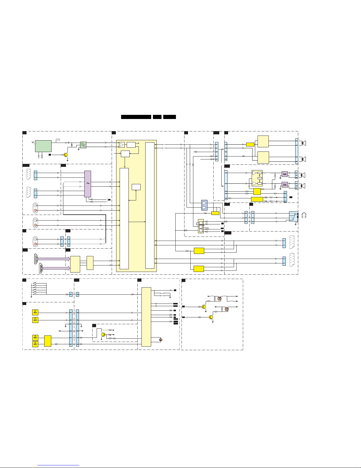
Block Diagrams, Test Point Overviews, and Waveforms
EN 27LC4.31E AA 6.
Block Diagram Audio
B5
AUDIO PROCESSING
B17
SIDE
CONNECTORS
D
SIDE AV
B2
HERCULES
B1
TUNER & IF
AUDIO
CONTROL
J
IR/LED/LIGHT-SENSOR
B2
HERCULES
C
AUDIO AMPLIFIER
(CLASS-D)
B16
B14
DIGITAL IO
B15A
SCART ANALOG-IO
D
SIDE AV
B17
SIDE CONNECTORS
E
KEYBOARD CONTROL
B17
SIDE CONNECTORS
B3
SYNC INTERFACE
B6
DC-DC CONVERTER
B14
DIGITAL IO
SA3
AUDIO
B15A
SCART ANALOG-IO
B12
HDMI
1001
4
3
2
1
LEFT
SPEAKER
RIGHT
SPEAKER
60
61
AUDOUTLSR
AUDOUTLSL
1K01
(1K04)
10 10
1304
(1M36)
12 12
HP_LOUT
HP_ROUT
HEADPHONE
HEAD_PH_L
HEAD_PH_R
7217
TDA15021H
1152
UV1318S
RF IN
TUNER
2156
11
4
5
SCL
SDA
QSS Mixer
AM Demod.
AM
1156
4
5
1
SIF1
SIF2
AD Conv.
Std Stereo
Decoder
21
1
1G02-1
21
1
1G01-1
21
1
SC1_L_RF_OUT
SC1_R_RF_OUT
AV1_Audio_INL
AV1_Audio_INR
34
35
SC2_L_MON_OUT
SC2_R_MON_OUT
AV2_Audio_INL
AV2_Audio_INR
21
1
62
63
36
37
29
30
33
IF-TER
IFOUT
F158
AUDIO
SELECT
ADC/DAC
AUDIO
CONTROL
Vol/Treb/
Bass
Features
DACs
I2S
Processor
QSS/FM
1310(1704)
3324(1705)
1311(1701)
1312(1702)
1313(1706)
Channel+
Channel-
Volume+
Volume-
Power
33
55
1870
(0345)
1K00
22
44
66
PC-TV-LED
LED_SEL
RC
+3V3STBY
PC-TV-LED
LED_SEL
RC_OUT
KEYBOARD
97
7217
TDA15021H
115
107
120
7430
+3v3STBY
+5VSW
3431
6430
114
SEL_IF_SDM
4204
SERVICE
SDM
116
STATUS_1
B15A
119
STATUS_2
MUTE
OUT_MUTE
102
EXT_MUTE
B5
POWER_DOWN
SOUND_ENABLE
111
SOUND-ENABLE
B5
122
SC_STANDBY
B6
G_16210_062.eps
030206
B1
HERCULES
6154
7151
3
SEL_IF_SDM
B2
MUTE
OUT_MUTE
MUTE
4211
4212
1J04
33
1002
11
POWER
COMPARATOR
7001
TDA8931T
OUT
HVPI
16
13
IN+
4
POWER
COMPARATOR
7000
TDA8931T
OUT
HVPI
16
13
IN+
4
88
7
AUDIO-R
SOUND-ENABLE
AUDIO-L
PHASE
INVERTER
SOUND-ENABLE
7606
7202
7201
1G01-1
6
2
1G02-1
6
2
1G02-2
66
88
L_FRONT_IN
R_FRONT_IN
SIDE_AudioINL
SIDE_AudioINR
53
54
1304
(1M36)
1K01
(1K04)
11
LIGHT-SENSOR
LSIPDP_DVB_SEMISTANDBY
1309(1703)
Menu
1684
(1M01)
22
1K02
(1M01)
KEYBOARD
+3V3STBY
P50_LIN2_ITV_IR_SW_RST
123
1202
24M576
127
AV2_DMMI_SW
7601
TS482ID
1
726
SC1_L
SC1_R
SC2_L
SC2_R
7
7004
11
10
1303
(1010)
7
1
2
11 11
HP_DET_R_DC1
HP_DET_R_DC_1
HP_DET_R_DC_1
EXT_MUTE
2
1
9
10
7602
74HC08PW
B16
B2
B2
6
8
SC1_L_RF_OUT
SC1_R_RF_OUT
SC2_L_MON_OUT
SC2_R_MON_OUT
OUT_MUTE
&
&
&
3
5
3432
RES
7756
3759
3750
+3V3STBY
+3V3SW
SC_STANDBY
7755
PANEL-PWR-CTL
3758
3755
LVDS_VCC
5756 5757
PAN_VCC
+12VSW
B8
B2
EXT 1
SCART 1
EXT 2
SCART 2
AUDIO
L/R IN
3
1
3
1
7758
7754
2
HD_AudioINL
HD_AudioINR
HD_AudioINL
HD_AudioINR
49
50
1302
(1002)
7F03
1
12
4
11
2
15
3
13
9
Analog_AudioSEL1
1F01
AUDIO
L/R IN
DVI_D_AudioINL
DVI_D_AudioINR
DVI_D_AudioINL
DVI_D_AudioINR
56
57
SIDE_AudioINL
SIDE_AudioINR
Analog_AudioINL
Analog_AudioINR
10
Analog_AudioSEL2
B7
7D03
TDA9975
7D04
UDA1334ATS
DAC
14
16
HDMI_AudioINL
HDMI_AudioINR
1
3
2
A5
A7
B7
HDMI
10-BIT
VIDEO
CONVERTER
HDMI_A
HDMI_B
1F02
1F03
19
1
18 2
19
1
18 2
FOR 26” & 32” ONLY
FOR 37”ONLY
7
9
8
3
1
1739
PWM
PWM
OSC
7700
TDA7490
5731
1736
1
2
3
5730
1735
1
2
3
1M02
7
TO 1M02
SUPPLY
A
SOUND
ENABLE
SOUND-ENABLE
AUDIO SUPPLY
PROT, CIRCUIT
PROT_AUDIOSUPPLY
7701÷7707
POR-CLASSD
PROT1
stbymute
10
6
18
3
23
AUDIO-L
AUDIO-R
3764
6703
3761
6702
-16 V-19V
+16 V+19V
7708÷7711
3717
3718
DCPROT
77
PROTECT_AUD
AUDIO-R
AUDIO-L
99
POR_AUDIO
OR
1
5
5702
5701
LED
SELECT
LED
GREEN
LED
RED
LIGHT
SENSOR
REMOTE
CONTROL
5700
LEFT
SPEAKER
RIGHT
SPEAKER
4205
B15A
B15B
B15A
B15B
( ) For 37” - 42”
( ) For 37” - 42”
( ) For 37” - 42”
( ) For 37” - 42”
AUDIO
L/R IN
HDMI 1
HDMI 2
EXT 1
SCART 1
EXT 2
SCART 2
EN 28LC4.31E AA 6.
Block Diagrams, Test Point Overviews, and Waveforms
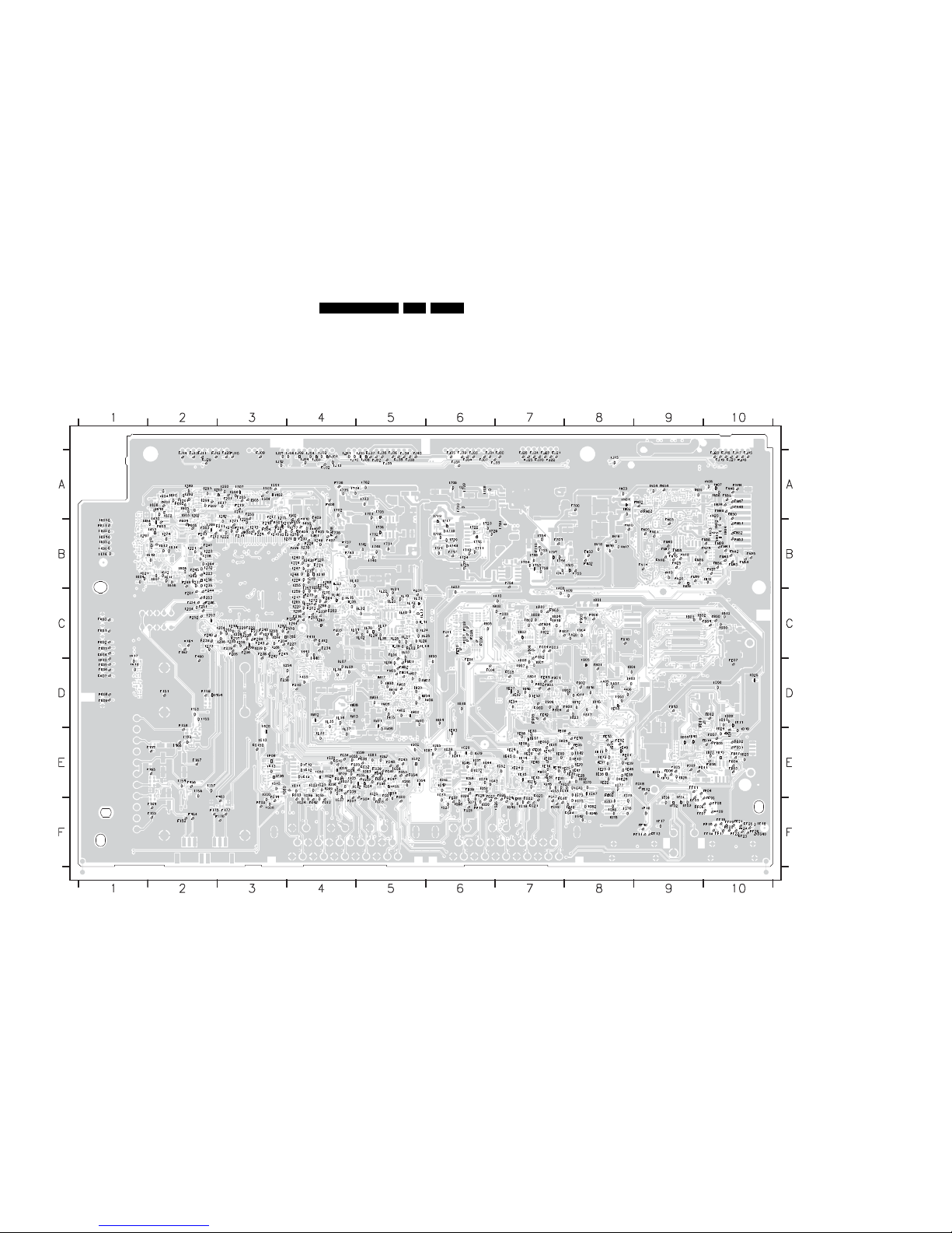
Test Point Overview Small Signal Board
G_16210_024.eps
170106
3139 123 6117.2
F151 D2
F152 F2
F154 F2
F155 F2
F156 E2
F157 E2
F158 D2
F159 D2
F160 C2
F161 C2
F162 C2
F163 E3
F164 F2
F165 E2
F166 E2
F167 E2
F175 F2
F176 F3
F177 F3
F201 A3
F202 A2
F203 A3
F204 C3
F205 C3
F206 C3
F207 C2
F208 C3
F209 C3
F210 D4
F211 B3
F212 B2
F213 B2
F214 B3
F215 B3
F216 C4
F217 A3
F218 B3
F219 A3
F220 B4
F221 B4
F222 C3
F223 B2
F224 B3
F225 B3
F226 B4
F227 C4
F228 B4
F229 C3
F230 B4
F231 B3
F232 B4
F233 C4
F234 C4
F235 C4
F236 D3
F237 C3
F238 C3
F239 C2
F240 C2
F241 C3
F242 C3
F243 C3
F244 C2
F245 B2
F246 C2
F247 B2
F248 C3
F249 B2
F250 C4
F251 C2
F252 C2
F253 C2
F254 C2
F255 C4
F256 C4
F257 C4
F258 A3
F262 C4
F263 C4
F264 C4
F404 B4
F405 B4
F406 A4
F407 B4
F408 B4
F409 A4
F410 B4
F411 C4
F412 C4
F501 B3
F502 B3
F503 B2
F504 B3
F505 B4
F601 A2
F602 A2
F603 B2
F604 B2
F605 B2
F700 A8
F701 B7
F710 B7
F717 B6
F736 A4
F737 B4
F738 B4
F743 B4
F754 B7
F755 B8
F800 C10
F801 D8
F802 D7
F803 C7
F804 C7
F900 D8
F901 D7
F902 D8
F903 D7
F904 D7
F905 C8
F906 C8
F907 C7
F908 D7
F909 D7
F910 C8
FB01 C10
FC00 C7
FC01 C7
FC02 C7
FC03 C7
FC04 D6
FC05 D7
FC06 C6
FC07 C6
FC08 C6
FC09 C6
FC10 C6
FC11 C6
FD01 E10
FD02 E10
FD03 E10
FD04 E10
FD05 E9
FD06 E9
FD07 E10
FD08 E10
FD09 E10
FD10 D9
FD11 E9
FD12 D10
FD13 D9
FD14 E10
FD15 E9
FD17 E10
FE00 E7
FE01 E8
FE02 E8
FE03 E7
FE04 D6
FE05 E8
FE06 E7
FE07 D10
FE08 E7
FE10 E8
FE11 D7
FE12 D7
FE13 E8
FF01 E9
FF02 F3
FF03 F9
FF04 E10
FF05 F10
FF06 F9
FF07 F9
FF08 F10
FF09 F10
FF10 F9
FF11 F9
FF12 E9
FF13 F9
FF14 F10
FF15 F6
FF16 F10
FF17 F10
FF18 F10
FF19 F10
FF20 F10
FF21 F10
FF22 F10
FF23 F10
FF24 F10
FF25 F10
FF26 F10
FG00 E5
FG01 E5
FG02 E8
FG03 F5
FG04 F5
FG05 F6
FG07 F4
FG08 E4
FG10 E4
FG11 E4
FG12 F4
FG13 E4
FG14 E3
FG15 E3
FG16 F7
FG17 E7
FG18 E9
FG19 F7
FG20 E7
FG21 F7
FG22 F7
FG24 F7
FG26 E7
FG27 E6
FG28 E6
FG32 E5
FG33 E4
FG34 E4
FG35 E5
FG36 E6
FG37 F6
FG38 E5
FG39 E5
FG40 F10
FG41 E5
FG42 F4
FG43 E5
FG44 F8
FG45 E5
FG47 E5
FG48 E5
FG49 E5
FG51 E5
FG53 E5
FG54 E5
FG56 E5
FJ00 A7
FJ01 A6
FJ02 A5
FJ03 A6
FJ04 A6
FJ05 A6
FJ06 A5
FJ07 A6
FJ08 A5
FJ09 A3
FJ10 A3
FJ11 A2
FJ12 A2
FJ13 A2
FJ14 A2
FJ15 A10
FJ16 A10
FJ17 A10
FJ18 A10
FJ19 A10
FJ20 A10
FJ21 A7
FJ22 A7
FJ23 A7
FJ24 A7
FJ25 A7
FJ26 A7
FJ27 A10
FJ28 A3
FJ29 A2
FJ30 A7
FJ31 A6
FJ32 A4
FJ33 A7
FJ34 A5
FJ35 A5
FJ36 A5
FJ37 A5
FJ38 A5
FJ39 A6
FJ40 A5
FK00 C1
FK01 C1
FK02 C1
FK03 C1
FK04 C1
FK05 D1
FK06 D1
FK07 D1
FK08 D1
FK09 D1
FK10 D1
FK11 B1
FL01 C5
FL02 C5
FL03 C4
FL04 C5
FM01 D5
FM02 D5
FM03 D5
FM04 D5
FM05 D5
FN01 B9
FN02 A9
FN03 B9
FN09 B9
FN10 B8
FN11 B9
FN12 A9
FN13 B10
FN15 B9
FN16 B9
FN17 B9
FN18 B9
FN19 B9
FN20 B9
FN24 B10
FN25 B9
FN32 B8
FN33 B8
FN34 A9
FN35 B9
FN36 B10
FN38 A10
FN39 A10
FN40 B9
FN41 B10
FN42 B10
FN43 B10
FN44 A10
FN46 A10
FN47 A10
FN48 A10
FN49 A10
FN50 A10
FN51 B10
FN52 B10
FN53 B10
FN54 B10
FN55 B10
FN56 B10
FN57 B10
FN58 B9
FN59 B10
I151 E2
I152 E2
I153 D2
I154 D3
I155 D2
I156 E2
I157 E2
I201 A2
I202 A2
I203 C2
I204 C3
I205 C3
I206 C3
I207 C3
I208 C3
I209 C3
I210 B3
I211 B3
I212 B3
I213 B3
I214 C3
I215 B3
I217 C4
I218 B4
I219 B4
I220 C4
I221 B2
I222 B3
I223 B2
I224 B4
I225 B3
I226 C3
I227 C3
I228 B4
I229 C3
I230 B4
I231 C3
I232 B2
I233 C3
I234 C2
I235 B2
I236 B2
I237 B2
I238 B2
I239 B4
I240 B4
I241 A3
I242 A3
I243 B4
I244 C4
I246 B4
I247 B4
I248 B4
I254 D4
I255 B4
I256 B4
I257 B4
I258 C3
I259 C4
I262 B2
I264 B2
I265 C4
I266 C4
I267 C4
I268 B4
I269 B2
I270 C4
I271 B4
I272 C4
I273 C2
I274 B2
I275 A3
I277 B4
I278 B4
I283 C3
I284 C3
I285 C4
I288 C3
I289 A2
I290 A3
I291 A2
I292 A2
I293 A3
I294 A2
I297 B1
I298 C4
I430 A2
I440 D4
I443 C4
I449 B4
I450 B4
I451 B4
I452 A3
I453 B2
I454 B1
I455 D4
I501 A3
I502 A4
I503 A3
I504 A3
I505 A3
I506 A3
I507 A3
I602 A2
I603 A2
I604 A2
I605 A2
I606 B2
I607 B2
I608 A2
I610 A2
I611 B2
I612 B2
I613 B2
I614 B2
I615 B2
I616 B2
I617 A3
I618 A2
I619 B2
I620 D3
I621 B1
I701 A5
I702 A4
I704 B7
I705 A5
I706 A6
I708 A6
I709 A6
I710 A6
I711 B6
I712 B6
I714 B6
I715 B6
I716 B6
I717 B6
I718 B6
I719 A6
I720 B6
I721 B6
I722 B6
I723 B6
I724 B6
I725 B6
I726 B6
I731 B5
I732 B5
I733 A5
I734 A4
I735 A4
I736 B5
I740 B5
I741 B5
I742 B5
I747 B7
I748 B7
I753 B7
I754 B7
I755 B7
I756 B7
I757 B7
I758 B7
I760 B8
I762 A5
I764 B7
I800 C6
I801 D7
I802 C7
I803 C7
I804 D8
I805 C6
I806 C7
I807 D7
I808 D7
I809 C7
I810 C7
I811 D10
I812 D8
I813 C10
I815 D8
I816 D8
I817 D8
I818 D6
I819 C7
I820 C8
I822 C7
I823 D8
I824 C7
I900 C10
I901 C8
I902 D8
I903 D8
I904 C8
I905 D8
I906 D7
I907 D7
I908 C7
IA00 D8
IA03 B6
IA05 D8
IA06 D8
IA07 D8
IA08 B7
IA09 C8
IA10 C7
IB02 C9
IB03 C9
ID00 D10
ID01 E9
ID08 E9
ID09 D10
ID10 E9
ID11 D10
ID13 E9
ID14 D8
ID15 E10
ID18 E10
ID19 E10
ID20 E10
ID22 E10
ID24 E10
ID25 D10
ID28 E9
IE00 E7
IE01 E8
IE02 E8
IE03 D8
IE04 E7
IE05 E7
IE06 E7
IE07 E7
IE08 E7
IE09 E7
IE10 E8
IE11 E8
IE12 E8
IE13 E7
IE14 E7
IE15 E7
IE16 E7
IE17 E7
IE18 E7
IE19 E7
IE20 E8
IE21 E7
IE22 E8
IE23 E8
IE24 E7
IE25 E8
IE26 E8
IE27 D7
IE28 E8
IE29 E7
IE30 E7
IE32 D7
IE33 D7
IE34 D7
IE35 E8
IE36 E8
IE37 E8
IE38 E8
IE39 E8
IE40 E7
IE42 E8
IE43 E6
IE44 D6
IE45 E7
IE46 D7
IE47 E8
IE48 E8
IE49 E8
IE50 E7
IF01 E9
IF02 F9
IF03 F9
IF04 F9
IF05 E5
IF06 E3
IF08 E3
IF09 E4
IF10 E4
IF12 E4
IF13 E3
IF14 E4
IF16 F9
IF17 F9
IF18 F10
IG00 E3
IG01 E5
IG02 E5
IG03 E5
IG04 E5
IG05 E4
IG06 E4
IG07 E4
IG08 F3
IG09 E4
IG10 E3
IG11 E4
IG12 E5
IG13 E3
IG14 E7
IG15 E7
IG16 E6
IG17 E6
IG18 F8
IG19 F7
IG20 E8
IG21 E7
IG22 E4
IG23 E4
IG24 E6
IG25 E5
IG26 F7
IG27 F6
IG28 E4
IG29 E6
IG30 E4
IG31 E6
IG32 E5
IG33 E7
IG34 F4
IG35 E4
IG36 E4
IG37 F4
IG38 E6
IG39 E6
IG40 E8
IG41 E6
IG42 F8
IG43 E6
IG44 E6
IG45 E6
IG46 F8
IG47 E8
IG48 F7
IG49 F7
IG50 F6
IG51 E6
IG52 E7
IG53 E4
IG54 E4
IG55 E4
IG56 E4
IG57 E6
IG58 E6
IG59 E5
IG60 E3
IG61 E5
IG62 E5
IG63 E5
IG64 E5
IG65 E6
IG66 E5
IG67 E6
IG68 F6
IG69 E4
IG70 E8
IG71 F6
IG72 E6
IG73 E8
IG74 E6
IG75 F8
IG76 F8
IG77 E8
IG78 F8
IG79 E8
IG80 F8
IG82 F8
IG83 F8
IJ01 A4
IJ02 A4
IJ03 A4
IJ04 A4
IJ05 A5
IJ06 A4
IJ07 A3
IJ08 A5
IJ09 A4
IJ10 A4
IJ11 A4
IJ12 A3
IJ13 A4
IJ14 A4
IJ15 A8
IK00 B1
IK01 B1
IK02 B1
IK03 B1
IK04 B1
IK05 B1
IK16 B1
IK17 C1
IK18 D1
IL01 C4
IL02 C5
IL03 C5
IL05 D4
IL06 D5
IL07 D4
IL09 C4
IL10 B4
IL11 C5
IL12 C5
IL13 C5
IL14 C5
IL15 C4
IL17 C5
IL18 C5
IL19 C5
IL20 C5
IL21 C5
IL22 C5
IL23 B4
IL24 C5
IL25 C5
IL26 C5
IL27 C5
IL28 C5
IL29 C5
IL30 C5
IL31 C5
IL32 C5
IL33 E4
IL34 D4
IL35 D4
IL36 D4
IL37 E4
IL38 C5
IL39 C5
IL40 C4
IM00 D5
IM01 D5
IM02 D5
IM03 D6
IM04 D5
IM05 D5
IM06 D6
IM07 D5
IM08 D4
IM09 E5
IM10 D5
IM11 D5
IM12 D4
IM13 D4
IM15 D5
IM16 D5
IM17 D5
IM18 D5
IM20 D5
IN01 A8
IN02 A8
IN03 A8
IN04 A9
IN05 A9
IN06 A10
IN07 A10
IN08 A10
IN09 B9
IN10 B9
IN11 B10
IN12 B10
IN13 B10
IN14 B10
IN15 B10
IN16 B8
IN17 B8
IN18 B8
IN19 B8
IN20 A10
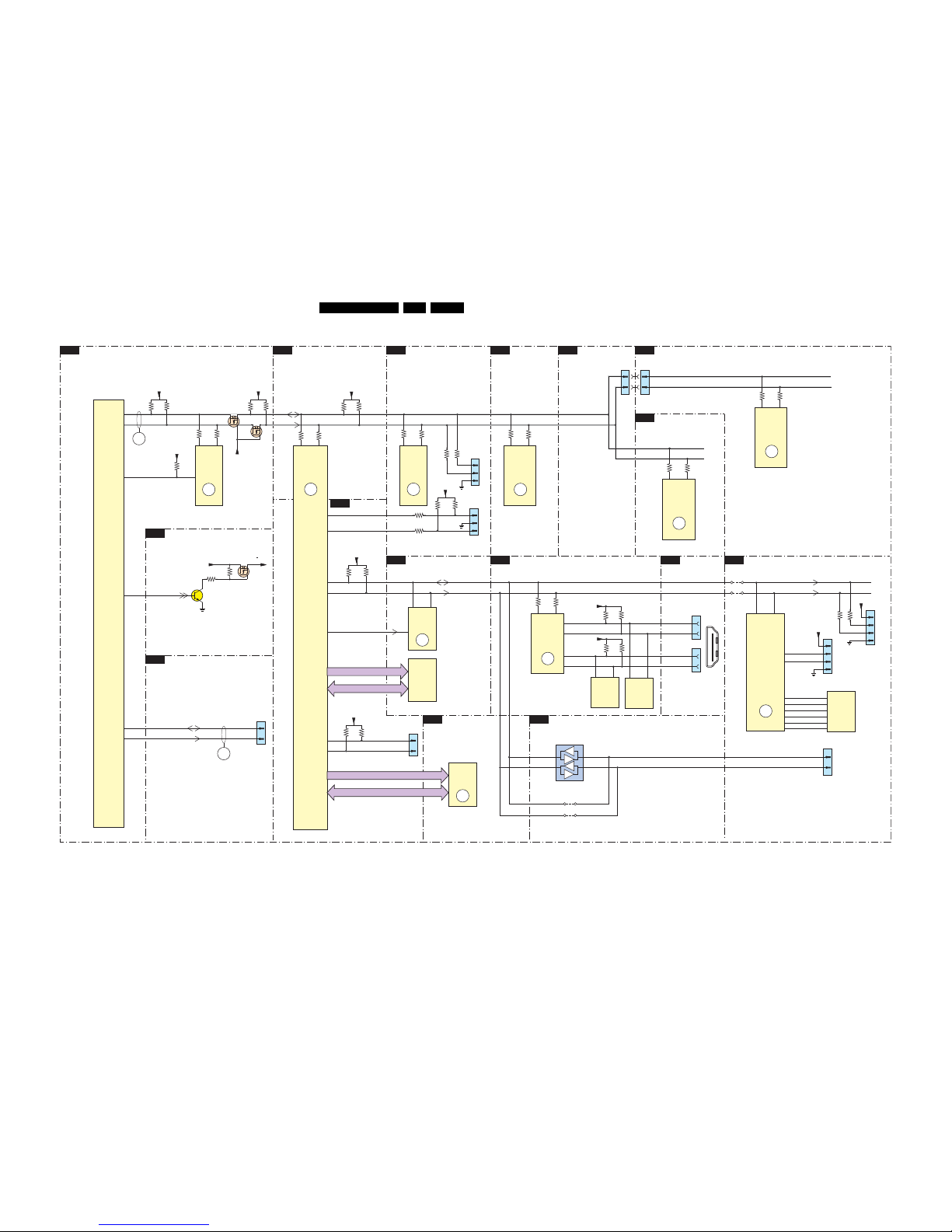
Block Diagrams, Test Point Overviews, and Waveforms
EN 29LC4.31E AA 6.
I2C Overview
7756
3759
3750
+3V3STBY
+3V3SW
SC_STANDBY
7758
7217
TDA15021H
I²C
HERCULES
B2
SCALER
B8
TUNER & IF
B1
COLUMBUS
B19
SYNC INTERFACEB3OTC-FLASH
T
ADC
B18
DMMI
B15B
SDRAM
B10
SCALER INTERFACE
B9
FLASH / CONTROL
B11
HDMI
B12
DIGITAL I/O
B14
PACIFIC3
B20
SCALER
B7
DC-DC CONVERTER
B6
SDA
SCL
109
HERCULES
SET
PROCESSOR
108
54
1102
UV1318S
TUNER
ERR
10
N1 N2
7801
GM1501H
SCALER
ERR
4
ERR
6
G_16210_063.eps
260906
+3V3STBY
3233
3232
56
7207
M24C16
EEPROM
NVM
ERR
9
NVM_WP_HERC
+3V3STBY
3249
104
1151
1
2
3
SERVICE
CONNECTOR
COMPAIR
5
6
7D01
M24C02
EEPROM
256x8
2x HDMI
CONNECTOR
3102
3101
SDA_IO
SCL_IO
5
6
7C01
M24C32
EEPROM
P3
P4
+3V3SW
3818
3817
ERR
8
NVM_WP_SCALER
7C03
M29W400D
ERROM
7B01
K4D263238F
SDRAM
ERR
14
ADDRESS
DATA
ADDRESS
DATA
AF5
SDA
SCL
7
1177
1
2
3
SERVICE
CONNECTOR
UART
UART_TX
UART_RX
3172
3173
M1
M2
2
1802
1
JTAG_TDI_SDA
JTAG_CLK_SCL
AF7
AD6
+3V3_IO
3838
3837
JTAG
I2C
FSDATA
FSADDR
OCMDATA
OCMADDR
7
SWHW_I2C_SDA
SWHW_I2C_SCL
1
1G03
2
Reserved
for DMMI
38 37
7L01
P3563M
ADC
ERR
7
3L19
3L18
A15
B15
7M00
T6TU5XBG
COLUMBUS
CTRL
ERR
11
3M14
3M15
ERR
17
198 200
7N00
T6TF4AFG
PACIFIC3
MISC
ERR
16
1N04
2
3
4
FOR
DEVELOPMENT
USE ONLY (N.S.)
SDA
SCL
1
+3V3SW
3N20
3N21
7A00
PCA9515ADP
1N17
(1G50)
31
30
3
2
6
7
TO
DISPLAY
3152
3151
112
113
19
1
18 2
75
74
7D03
TDA9975
HDMI
PANELLINK
RECEIVER
ERR
13
3D05
3D06
1F03
16
15
+5VHDMI_A
3D09
3D01
J16
J15
DOC_SCLB
DOC_SDAB
+3V3STBY
3170
3171
SDA_DMA_BUS1_DISP
SDA_DMA_BUS1_DISP
FOR PDP ONLY
(Depending on screen manufacturer)
4A01
4A00
RES
7221
7220
+3V3SW
3298
3297
+3V3SW
1442
14 14
1000
13 13
86 85
7001
SAA5801H/
TV
CONTROL
ERR
15
3016
3015
+3V3STBY
3902
3901
5
6
7D00
M24C02
EEPROM
256x8
1F02
16
15
K16
K15
DOC_SCLA
DOC_SDAA
+5VHDMI_B
3D10
3D03
4N30
4N31
(OPTIONAL PIXEL+)
SDA_PF3
SCL_PF3
1N03
2
3
4
FOR PACIFIC3
PROGRAMMING (N.S.)
SSDA
SSCL
1
+3V3SW
202
204
7N02
M25P05
Flash
512k
SPI_SO
SPI_SCK
192
191
SPI_CS
SPI_WP
194
188
SPI_RST
SPI_SI
187
193
5
6
1
3
7
2
(Only For 37” - 42” Sets)
122
3248
3247
3904
3903
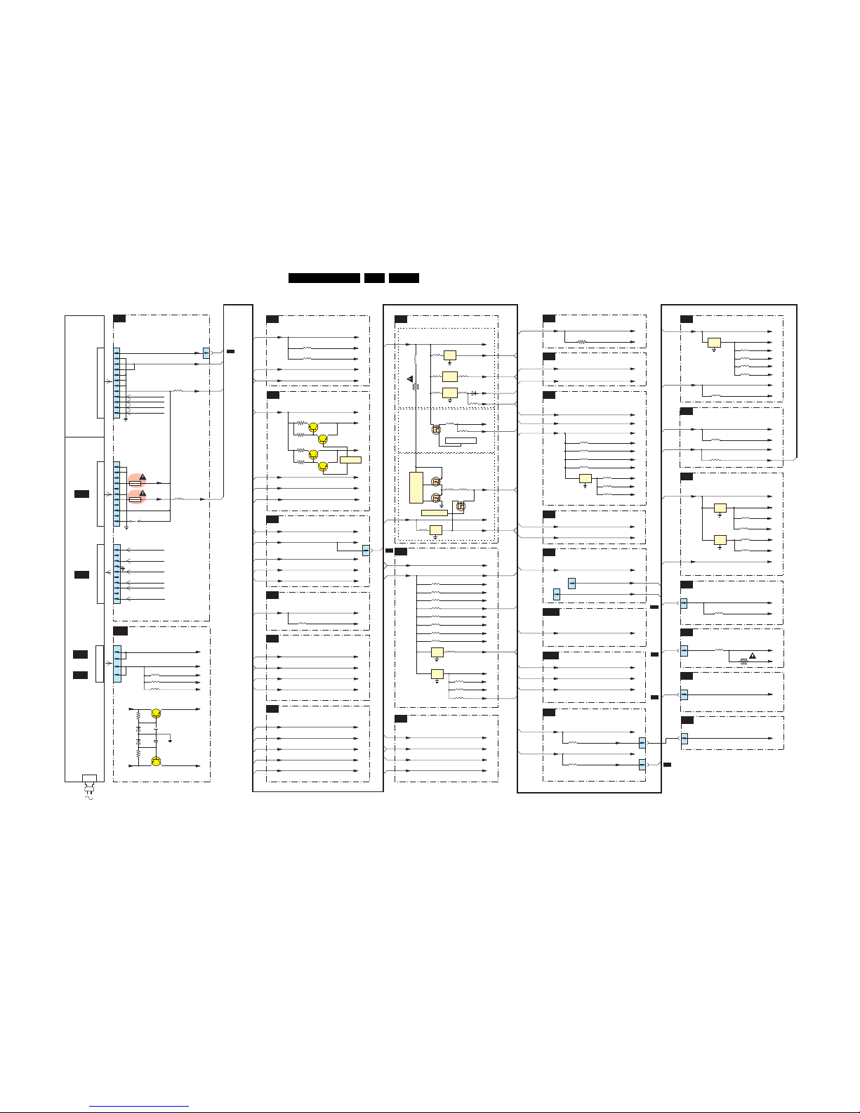
EN 30LC4.31E AA 6.
Block Diagrams, Test Point Overviews, and Waveforms
Supply Voltage Overview
B12
B18
B6
B6
B16
TOP CONNECTORS
B1
TUNER & IF
B2
HERCULES
B3
SYNC INTERFACE
B4
AUDIO DELAY LINE
(FOR PDP SETS ONLY)
B5
AUDIO PROCESSING
B7
SCALER
B8
SCALER
B10
SDRAM
B11
FLASH / CONTROL
B12
HDMI
B13
MUX-SYNC INTERFACE
B14
DIGITAL IO
B15A
SCART ANALOG IO
B18
ADC
B19
COLUMBUS
B20
PACIFIC3
B6
DC-DC CONVERTER
B15B
DMMI
C
CLASS D AUDIO AMPLIFIER
D
SIDE-AV
J
IR / LED / LIGHT-SENSOR
T
OTC-FLASH
(FOR 1000pg TXT)
B17
SIDE CONNECTORS
B9
SCALER INTERFACE
SA3
AUDIO
SUPPLY
PANEL 26”- 32”
(PSU)
SUPPLY LINE OVERVIEW
1
1J02
2
3
4
5
6
7
8
9
10
11
12
LAMP_ON_OFF
BACKLIGHT_CTRL
STANDBY
POWER_DOWN
+3V3STBY
VP
+12V
SW
+5VSW
+5VSW
+5VSW_b
+5VSW_a
5152
5153
+3V3STBY
+3V3STBY
+1V8_A
+3V3STBY
+3V3STBY
+5VSW
+5VSW
+8VSW_TV
+8VSW_TV
7215
3265
7216-1
3264
+1V8_B
7217
3263
7216-2
3262
+5VSW
+5VSW
+3V3STBY
+3V3STBY
+3V3SW
+3V3SW
+5VSWI
+5VSWI
+5VD
5501
+3V3SW
+3V3SW
+3V3STBY
+3V3STBY
+5VSW
+5VSW
+5V
+5V
+1V8_CORE
+1V8_CORE
+2V5_DDR
+2V5_DDR
+3V3SW
+3V3SW
+3V3_IO
+3V3_IO
+3V3_PLL
+3V3_PLL
+3V3SW
+3V3SW
+1V8
3V3_PLL
5900
3V3_ADC
5901
3V3_DVI
5902
3V3_IO
5903
3V3_LBADC
5904
3V3_LVD
SA
5905
3V3_LVD
SB
5906
3V3_LVD
S
5907
+2V5_DDR
5908
7900
IN OUT
COM
7901
IN OUT
COM
5909
5910
5911
+1V8_ADC
+1V8_DV1
+1V8_CORE
+2V5_DDR
+2V5_DDR
FSVREF
3B01
+3V3_IO
+3V3_IO
+3V3SW
+3V3SW
+3V3SW
+3V3SW
+3V3SW
+3V3SW
+5VSWI
+5VSWI
+5VSWI
+5VSWI
18
1F03
+5VHDMI_B
+5VSW
+5VSW
+5VSWIA
+5VSWIA
+3V3SWB
7L02
IN OUT
COM
+3V3SW
+3V3SW
+3V3SWA
5M03
+5VSWI
+5VSWI
+5VSWIA
5M04
+3V3SW
+3V3SW
+1V5
LVDS_VCC
LVDS_VCC
+2V5PLL
7N03
IN OUT
COM
5N03
+2V5VDD
1
1J01
(1M46)
2
3
4
5
6
7
8
9
10
11
+12VUFD
+5V_UFD
5J03
1J07
1J08
N.C
.
N.C
.
N.C
.
N.C
.
4J01
+5V
37”/42” SETS
1J03
1
1
1J00
(1M0
3)
2
3
4
5
6
7
8
9
10
STANDBY
FAN_SPEED
BACKLIGHT_CTRL
N.C
.
LAMP_ON_OFF
POWER_UP_OK
N.C
.
N.C
.
PROTECT_AUD
UFD CONTROL
C
1003
B1,B2,B
3,
B5,B8,B9,
B15b
B3,B6
B5,B6,B9
B6
B6,B16
B16
B6
B6
B6
B6
B16
B6
B6
B8
B6
B15b
B4,B9,B19
B19
B6
B6
B20
B6
B6
26” SETS
+12V
SW
+3V3STBY
7708
IN OUT
COM
+5V
+5V
5704
+8VSW_TV
7738
IN OUT
COM
5738
7754
LVDS_VCC
7758
+3V3SW
PANEL-PWR-CTL
5752
DC/DC
Converter
7752
5753
5754
+5VSWI
5730
PWR
REG
7730
5733
+VTUN
+5VSW
5737
5757
6735
B16
B16
5709
(For 37”-50”
Large Screen)
DVI
5J04
B7,B10
B8
B8
B8
B6
B6
B6,B16
B6
B6
B8
B6
B6
B6
B6
B7,B11
B13,B19,B20
B8
5700
B6
PAN_VCC
(For 26”-42” Screen)
HERCULE
S
RES
X200
X002
+3V3SW
+3V3SW
+12V
SW
+12V
SW
+5V
+5V
+12V
SW
7758
5717
5713
STEP
DOWN
CONTR
3718
7754
SC_STANDBY
(Supply to T
uner & Herc
ules)
+3V3STBY
+3V3STBY
B16
VDDA_3V3PLL
5D06
VDDA_3V3
5D00
VDDD_
3V3
5D01
VDDI_
3V3
5D02
VDDC_1V
8
5D05
7D02
IN OUT
COM
5D03
5D04
VDDA_1V8
VDDD_1V
8
18
1F02
+5VHDMI_A
DVI
+3V3STBY
+3V3STBY
+5VSW
+5VSW
+8VSW_TV
+8VSW_TV
5L01
5L11
VDDP
VADC
VMPLL
5L17
VPLL
+2V5_DDR
+2V5_DDR
VDDC
5L21
B8
7N04
IN OUT
COM
5N04
1V5CORE
5N05
+1V5PLL
5N06
3001
5001
3
B16
7
B17
5
1J03
1K01
VP
VP_SGN
+5VSW
+3V3STBY
1870
1304
1003
5001
6
B3
1442
+3V3SW
+3V3_INTO
TC
1000
(OPTIONAL)
+3V3STBY
+3V3STBY
+5VSW
+5VSW
1K00
5
1K01
7
+3V3STBY_1
+5VSW_1
B6,B16
B6
D
1304
+5VHDMI_A
+5VHDMI_A
+5VHDMI_B
+5VHDMI_B
B14
B14
5L19
B18
+3V3SW
+3V3SW
+3V3STBY
+3V3STBY
+5VSWI
+5VSWI
+5V
+5V
B16
B6
B2,B3,B5,B7,
B8,B9,B11,B12
B12
B13
B15a,B15
b,
B17
B1,B2,B3,B5,
B8,B9,B15b
B1,B2,B
3,B5
B6
B16
B6
B2
B6
B16
B6
B6
B6
B6
B6
B7
B7
1M46
B6
G_16210_064.ep
s
260906
B1
+VTUN
+VTUN
1M02
2
6
+16V+19V
-16V-19V
-Vf21
-Vf11
-Vf1
+16V+19V
-16V-19V
Vp
Vm
A2
1M02
TO 1M02
SUPPLY 37”
1
5
5723
5707
5711
3760
3759
7712
7713
2797
2798
67106711
SA1
TO 1M03
STBY-SUPPLY
SA1
TO 1M46
STBY-SUPPLY
SUPPLY
PANEL 37”/42”
(PSU)
1M03
5K00
5K01
(Only For 26” - 32” Sets)
(Only For 37”/42” Sets)
(Only For 26” - 32” Sets)
A4
TO 1M02
SUPPLY 42”
1442
6
T
1000
 Loading...