

Page 1

Colour TV Chassis
MG8
TCM1.0E
LA
MG8
I_17930_000.eps
240408
Contents Page Contents Page
1. Technical Specifications, Connections, and Chassis
Overview 2
2. Safety Instructions, Warnings, and Notes 5
3. Directions for Use 6
4. Mechanical Instructions 7
5. Service Modes, Error Codes, and Fault Finding 13
6. Block Diagrams, Test Point Overview, and
Waveforms
Wiring Diagram (not available yet) 19
Block Diagram MT8200 20
7. Circuit Diagrams and PWB Layouts Diagram PWB
Main Power Supply (19" & 20") (A)21 22
Main Power Supply (26") (A1)23 25
Standby Power Supply (26") (A2)24 26
SSB: Index /GPIO List /LDO (B01)27 38-39
SSB: MT8200 LQFP256 (B02)28 38-39
SSB: DDR Memory & Flash (B03)29 38-39
SSB: VGA Input (B04)30 38-39
SSB: LVDS /TTL Interface (B05)31 38-39
SSB: Tuner Block (B06)32 38-39
SSB: SCART Input Interface (B07)33 38-39
SSB: AV & S-Video & PC Audio Input (B08)34 38-39
SSB: Audio / Power / Headphone (B09)35 38-39
SSB: HDMI Input MT8293 (B10)36 38-39
SSB: DC DC / MCU for Stby/Protect (B11)37 38-39
Keyboard Control Panel (E)40 40
Inverter Panel (I)41 42
IR LED Panel (J)43 43
8. Alignments 45
9. Circuit Descriptions, Abbreviation List, and IC Data
Sheets 46
Abbreviation List 48
IC Data Sheets 51
10. Spare Parts List & CTN Overview 55
11. Revision List 55
©
Copyright 2008 Koninklijke Philips Electronics N.V.
All rights reserved. No part of this publication may be reproduced, stored in a
retrieval system or transmitted, in any form or by any means, electronic,
mechanical, photocopying, or otherwise without the prior permission of Philips.
Published by JY 0871 BU TV Consumer Care Printed in the Netherlands Subject to modification EN 3122 785 17931
Page 2

EN 2 TCM1.0E LA1.
Technical Specifications, Connections, and Chassis Overview
1. Technical Specifications, Connections, and Chassis Overview
Index of this chapter:
1.1 Technical Specifications
1.2 Connection Overview
1.3 Chassis Overview
Notes:
• Figures can deviate due to the different set executions.
• Specifications are indicative (subject to change).
1.1 Technical Specifications
1.1.1 Vision
Display type : LCD
Screen size : 19" (48 cm), 4 : 3
: 20" (51 cm), 4 : 3
: 26" (66 cm), 16 : 9
Resolution (H × V pixels) : 640 × 480 (20")
Light output (cd/m
Contrast ratio : 800 : 1
Viewing angle (H × V degrees) : 170 × 160 (19")
Tuning system : PLL
Colour systems : PAL, SECAM
Video playback : PAL, SECAM, NTSC
Tuner bands : UHF, VHF, S & Hyper
Supported Computer Formats
60 Hz : 640 × 480
60 Hz : 800 × 600
60 Hz : 1024 × 768
60 Hz : 1280 × 1024 (19/26")
60 Hz : 1366 × 768 (26")
50 Hz, 75 Hz : 1440 × 900 (26")
Supported Video Formats
60 Hz : 480i
60 Hz : 480p
50 Hz : 576i
50 Hz : 576p
50 Hz, 60 Hz : 720p
50 Hz, 60 Hz : 1080i
2
) : 300 (20")
: 500 (26")
: 178 × 178 (20")
: 160 × 160 (26")
1.1.3 Miscellaneous
Power supply
- Mains voltage (V
- Mains frequency (Hz) : 50, 60
Power consumption (W) : 50 (19")
Stand-by (W) : < 0.3
Dimensions (W × H × D in mm) : 473 × 353 × 69 (19")
Weight (kg) : 4.9 (19")
) : 100 to 240
AC
: 45 (20")
: 80 (26")
: 470 × 406 × 71 (20")
: 671 × 458 × 90 (26")
: 5.8 (20")
: 7.7 (26")
1.1.2 Sound
Sound systems : Mono
Maximum power (W) : 2 × 3 (19")
:Stereo
:2 × 3 (20")
:2 × 5 (26")
Page 3

Technical Specifications, Connections, and Chassis Overview
1.2 Connection Overview
Figure 1-1 Rear I/O connections
I_17930_001.eps
220408
EN 3TCM1.0E LA 1.
Note: The following connector colour abbreviations are used
(acc. to DIN/IEC 757): Bk= Black, Bu= Blue, Gn= Green, Gy=
Grey, Rd= Red, Wh= White, and Ye= Yellow.
1.2.1 Rear Connections
1, Mini Jack: VGA Audio - In
Bk - Audio L/R 0.5 V
/ 10 kohm jq
RMS
2, HDMI: Digital Video, Digital Audio - In
19
18 2
1
E_06532_017.eps
250505
Figure 1-2 HDMI (type A) connector
1 -D2+ Data channel j
2 -Shield Gnd H
3 -D2- Data channel j
4 -D1+ Data channel j
5 -Shield Gnd H
6 -D1- Data channel j
7 -D0+ Data channel j
8 -Shield Gnd H
9 -D0- Data channel j
10 - CLK+ Data channel j
11 - Shield Gnd H
12 - CLK- Data channel j
13 - n.c.
14 - n.c.
15 - DDC_SCL DDC clock j
16 - DDC_SDA DDC data jk
17 - Ground Gnd H
18 - +5V j
19 - HPD Hot Plug Detect j
20 - Ground Gnd H
3, VGA PC: Video RGB - In and Service UART
1
5
6
11
10
15
E_06532_002.eps
171108
Figure 1-3 VGA Connector
1 -Video Red 0.7 V
2 -Video Green 0.7 V
3 -Video Blue 0.7 V
4-n.c.
/ 75 ohm j
PP
/ 75 ohm j
PP
/ 75 ohm j
PP
5 -Ground Gnd H
6 -Ground Red Gnd H
7 -Ground Green Gnd H
8 -Ground Blue Gnd H
9 - +5V_dc +5 V j
10 - Ground Sync Gnd H
11 - n.c.
12 - DDC_SDA DDC data j
13 - H-sync 0 - 5 V j
14 - V-sync 0 - 5 V j
15 - DDC_SCL DDC clock j
4, EXT 1: Video RGB/YC - In, CVBS - In/Out, Audio - In/Out
21
20
E_06532_001.eps
2
1
050404
Figure 1-4 SCART connector
1 - Audio R 0.5 V
2 - Audio R 0.5 V
3 - Audio L 0.5 V
/ 1 kohm k
RMS
/ 10 kohm j
RMS
/ 1 kohm k
RMS
4 - Ground Audio Gnd H
5 - Ground Blue Gnd H
6 - Audio L 0.5 V
7 - Video Blue/C-out 0.7 V
8 - Function Select 0 - 2 V: INT
/ 10 kohm j
RMS
/ 75 ohm jk
PP
4.5 - 7 V: EXT 16:9
9.5 - 12 V: EXT 4:3 j
9 - Ground Green Gnd H
10 - Easylink P50 0 - 5 V / 4.7 kohm jk
11 - Video Green 0.7 V
12 - n.c.
/ 75 ohm j
PP
Page 4
EN 4 TCM1.0E LA1.
13 - Ground Red Gnd H
14 - Ground P50 Gnd H
15 - Video Red/C 0.7 V
16 - Status/FBL 0 - 0.4 V: INT
17 - Ground Video Gnd H
18 - Ground FBL Gnd H
19 - Video CVBS 1 V
20 - Video CVBS/Y 1 V
21 - Shield Gnd H
5, EXT 2: Cinch: Video YPbPr - In, Audio - In
Gn - Video Y 1 V
Bu -Video Pb 0.7 V
Rd - Video Pr 0.7 V
Ye -Video CVBS 1 V
Wh - Audio L 0.5 V
Rd - Audio R 0.5 V
6, EXT 3 Input: S-Video (Hosiden): Video Y/C - In
1 - Ground Y Gnd H
2 - Ground C Gnd H
3 - Video Y 1 V
4 - Video C 0.3 V
7, Aerial - In
- - IEC-type (EU) Coax, 75 ohm D
/ 75 ohm j
PP
1 - 3 V: EXT / 75 ohm j
/ 75 ohm k
PP
/ 75 ohm j
PP
/ 75 ohm jq
PP
/ 75 ohm jq
PP
/ 75 ohm jq
PP
/ 75 ohm jq
PP
/ 10 kohm jq
RMS
/ 10 kohm jq
RMS
/ 75 ohm j
PP
P / 75 ohm j
PP
Technical Specifications, Connections, and Chassis Overview
8, Mini Jack: Audio Head phone - Out
Bk - Head phone 32 - 600 ohm / 10 mW ot
1.3 Chassis Overview
SMALL SIGNAL BOARD
B
MAIN POWER SUPPLY
A1
INVERTER PANEL
KEYBOARD
CONTROL PANEL
STANDBY POWER
SUPPLY UNIT
(OPTIONAL)
IR LED PANEL
I
E
A2
J
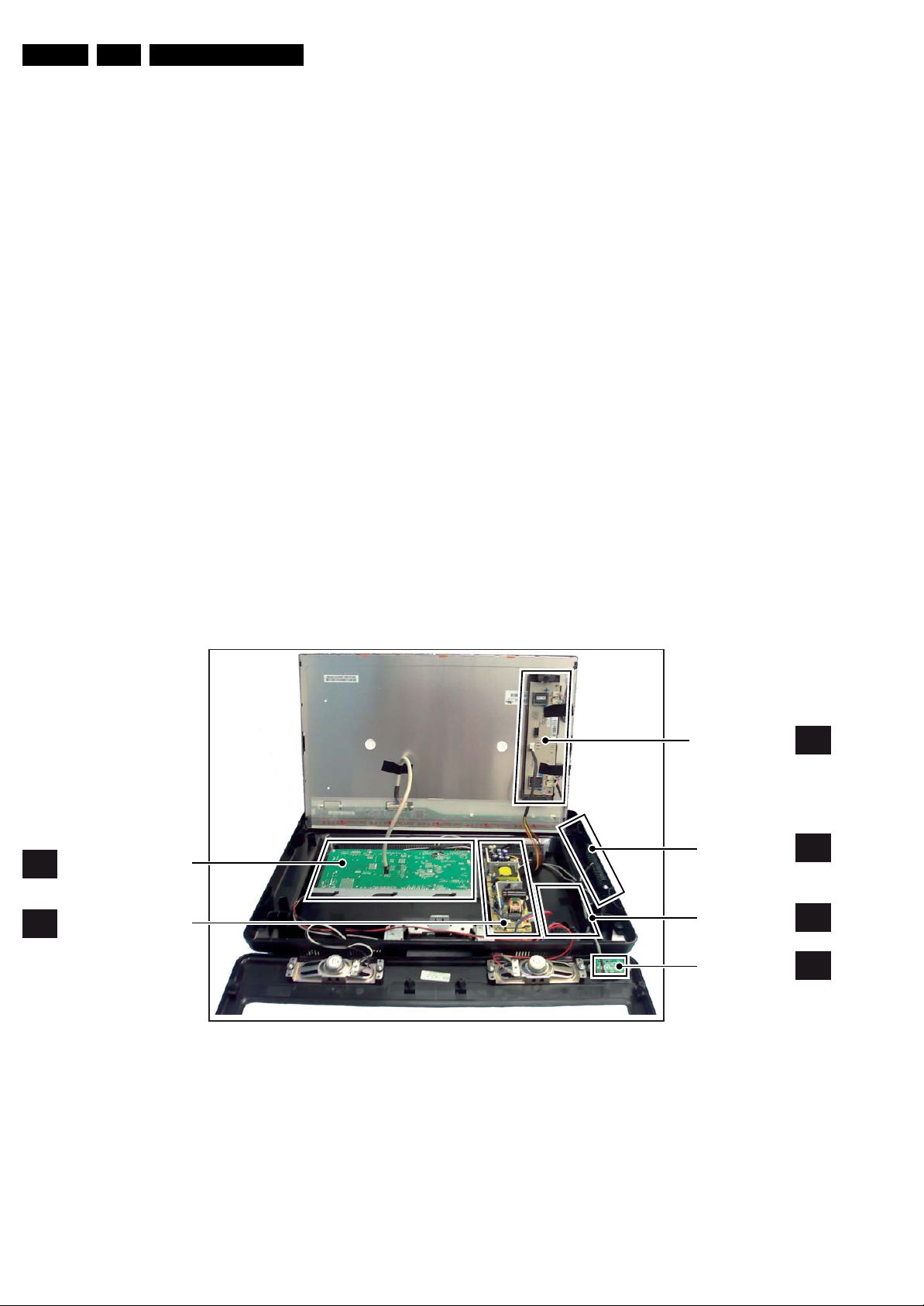
Figure 1-5 PWB/CBA locations
I_17930_068.eps
250408
Page 5

Safety Instructions, Warnings, and Notes
2. Safety Instructions, Warnings, and Notes
EN 5TCM1.0E LA 2.
Index of this chapter:
2.1 Safety Instructions
2.2 Warnings
2.3 Notes
2.1 Safety Instructions
Safety regulations require the following during a repair:
• Connect the set to the Mains/AC Power via an isolation
transformer (> 800 VA).
• Replace safety components, indicated by the symbol h,
only by components identical to the original ones. Any
other component substitution (other than original type) may
increase risk of fire or electrical shock hazard.
Safety regulations require that after a repair, the set must be
returned in its original condition. Pay in particular attention to
the following points:
• Route the wire trees correctly and fix them with the
mounted cable clamps.
• Check the insulation of the Mains/AC Power lead for
external damage.
• Check the strain relief of the Mains/AC Power cord for
proper function.
• Check the electrical DC resistance between the Mains/AC
Power plug and the secondary side (only for sets that have
a Mains/AC Power isolated power supply):
1. Unplug the Mains/AC Power cord and connect a wire
between the two pins of the Mains/AC Power plug.
2. Set the Mains/AC Power switch to the “on” position
(keep the Mains/AC Power cord unplugged!).
3. Measure the resistance value between the pins of the
Mains/AC Power plug and the metal shielding of the
tuner or the aerial connection on the set. The reading
should be between 4.5 Mohm and 12 Mohm.
4. Switch “off” the set, and remove the wire between the
two pins of the Mains/AC Power plug.
• Check the cabinet for defects, to prevent touching of any
inner parts by the customer.
2.2 Warnings
• Where necessary, measure the waveforms and voltages
with (D) and without (E) aerial signal. Measure the
voltages in the power supply section both in normal
operation (G) and in stand-by (F). These values are
indicated by means of the appropriate symbols.
2.3.2 Schematic Notes
• All resistor values are in ohms, and the value multiplier is
often used to indicate the decimal point location (e.g. 2K2
indicates 2.2 kohm).
• Resistor values with no multiplier may be indicated with
either an “E” or an “R” (e.g. 220E or 220R indicates
220 ohm).
• All capacitor values are given in micro-farads (μ=× 10
nano-farads (n =× 10
• Capacitor values may also use the value multiplier as the
decimal point indication (e.g. 2p2 indicates 2.2 pF).
• An “asterisk” (*) indicates component usage varies. Refer
to the diversity tables for the correct values.
• The correct component values are listed in the Spare Parts
List. Therefore, always check this list when there is any
doubt.
2.3.3 BGA (Ball Grid Array) ICs
Introduction
For more information on how to handle BGA devices, visit this
URL: www.atyourservice.ce.philips.com (needs subscription,
not available for all regions). After log-in, select “Magazine”,
then go to “Repair downloads”. Here you will find Information
on how to deal with BGA-ICs.
BGA Temperature Profiles
For BGA-ICs, you must use the correct temperature-profile,
which is coupled to the 12NC. For an overview of these profiles,
visit the website www.atyourservice.ce.philips.com (needs
subscription, but is not available for all regions)
You will find this and more technical information within the
“Magazine”, chapter “Repair downloads”.
For additional questions please contact your local repair help
desk.
-9
), or pico-farads (p =× 10
-12
-6
),
).
• All ICs and many other semiconductors are susceptible to
electrostatic discharges (ESD w). Careless handling
during repair can reduce life drastically. Make sure that,
during repair, you are connected with the same potential as
the mass of the set by a wristband with resistance. Keep
components and tools also at this same potential.
• Be careful during measurements in the high voltage
section.
• Never replace modules or other components while the unit
is switched “on”.
• When you align the set, use plastic rather than metal tools.
This will prevent any short circuits and the danger of a
circuit becoming unstable.
2.3 Notes
2.3.1 General
• Measure the voltages and waveforms with regard to the
chassis (= tuner) ground (H), or hot ground (I), depending
on the tested area of circuitry. The voltages and waveforms
shown in the diagrams are indicative. Measure them in the
Service Default Mode (see chapter 5) with a colour bar
signal and stereo sound (L: 3 kHz, R: 1 kHz unless stated
otherwise) and picture carrier at 475.25 MHz for PAL, or
61.25 MHz for NTSC (channel 3).
2.3.4 Lead-free Soldering
Due to lead-free technology some rules have to be respected
by the workshop during a repair:
• Use only lead-free soldering tin Philips SAC305 with order
code 0622 149 00106. If lead-free solder paste is required,
please contact the manufacturer of your soldering
equipment. In general, use of solder paste within
workshops should be avoided because paste is not easy to
store and to handle.
• Use only adequate solder tools applicable for lead-free
soldering tin. The solder tool must be able:
– To reach a solder-tip temperature of at least 400°C.
– To stabilize the adjusted temperature at the solder-tip.
– To exchange solder-tips for different applications.
• Adjust your solder tool so that a temperature of around
360°C - 380°C is reached and stabilized at the solder joint.
Heating time of the solder-joint should not exceed ~ 4 sec.
Avoid temperatures above 400°C, otherwise wear-out of
tips will increase drastically and flux-fluid will be destroyed.
To avoid wear-out of tips, switch “off” unused equipment or
reduce heat.
• Mix of lead-free soldering tin/parts with leaded soldering
tin/parts is possible but PHILIPS recommends strongly to
avoid mixed regimes. If this cannot be avoided, carefully
clear the solder-joint from old tin and re-solder with new tin.
Page 6
EN 6 TCM1.0E LA3.
2.3.5 Alternative BOM identification
The third digit in the serial number (example:
AG2B0335000001) indicates the number of the alternative
B.O.M. (Bill Of Materials) that has been used for producing the
specific TV set. In general, it is possible that the same TV
model on the market is produced with e.g. two different types
of displays, coming from two different suppliers. This will then
result in sets which have the same CTN (Commercial Type
Number; e.g. 28PW9515/12) but which have a different B.O.M.
number.
By looking at the third digit of the serial number, one can
identify which B.O.M. is used for the TV set he is working with.
If the third digit of the serial number contains the number “1”
(example: AG1B033500001), then the TV set has been
manufactured according to B.O.M. number 1. If the third digit is
a “2” (example: AG2B0335000001), then the set has been
produced according to B.O.M. no. 2. This is important for
ordering the correct spare parts!
For the third digit, the numbers 1...9 and the characters A...Z
can be used, so in total: 9 plus 26= 35 different B.O.M.s can be
indicated by the third digit of the serial number.
Identification: The bottom line of a type plate gives a 14-digit
serial number. Digits 1 and 2 refer to the production centre (e.g.
AG is Bruges), digit 3 refers to the B.O.M. code, digit 4 refers
to the Service version change code, digits 5 and 6 refer to the
production year, and digits 7 and 8 refer to production week (in
example below it is 2006 week 17). The 6 last digits contain the
serial number.
Directions for Use
MODEL :
PROD.NO:
2.3.6 Board Level Repair (BLR) or Component Level Repair (CLR)
If a board is defective, consult your repair procedure to decide
if the board has to be exchanged or if it should be repaired on
component level.
If your repair procedure says the board should be exchanged
completely, do not solder on the defective board. Otherwise, it
cannot be returned to the O.E.M. supplier for back charging!
2.3.7 Practical Service Precautions
• It makes sense to avoid exposure to electrical shock.
• Always respect voltages. While some may not be
32PF9968/10
AG 1A0617 000001
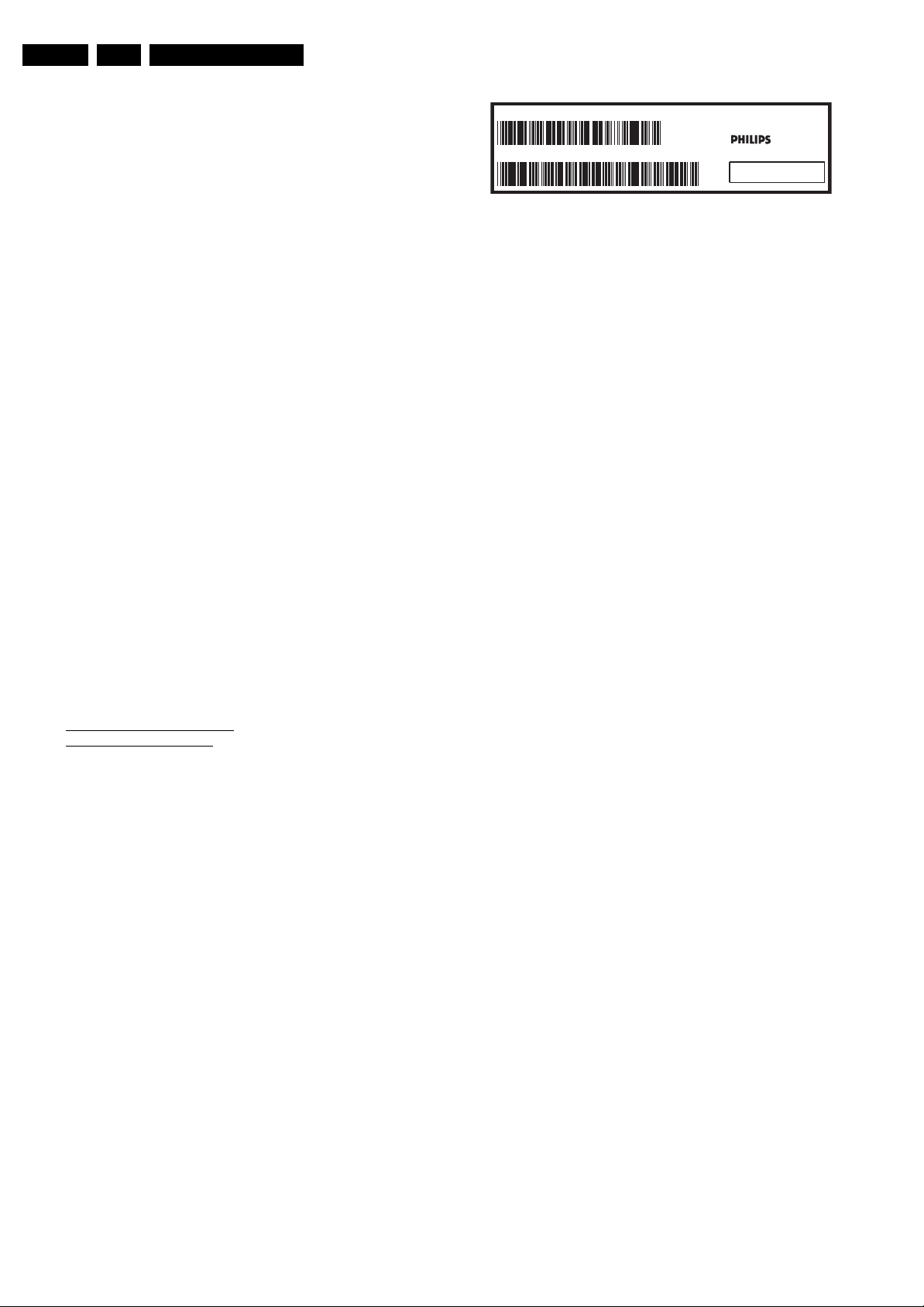
Figure 2-1 Serial number (example)
While some sources are expected to have a possible
dangerous impact, others of quite high potential are of
limited current and are sometimes held in less regard.
dangerous in themselves, they can cause unexpected
reactions that are best avoided. Before reaching into a
powered TV set, it is best to test the high voltage insulation.
It is easy to do, and is a good service precaution.
MADE IN BELGIUM
220-240V 50/60Hz
VHF+S+H+UHF
S
~
BJ3.0E LA
E_06532_024.eps
128W
260308
3. Directions for Use
You can download this information from the following websites:
http://www.philips.com/support
http://www.p4c.philips.com
Page 7

4. Mechanical Instructions
Mechanical Instructions
EN 7TCM1.0E LA 4.
Index of this chapter:
4.1 Cable Dressing
4.2 Service Positions
4.3 Assy/Panel Removal
4.4 Set Re-assembly
4.1 Cable Dressing
Notes:
• Figures below can deviate slightly from the actual situation,
due to the different set executions.
• Follow the disassemble instructions in described order.
They apply mostly to the 26" model unless otherwise
specified, but the described method is comparable for the
other screen sizes.
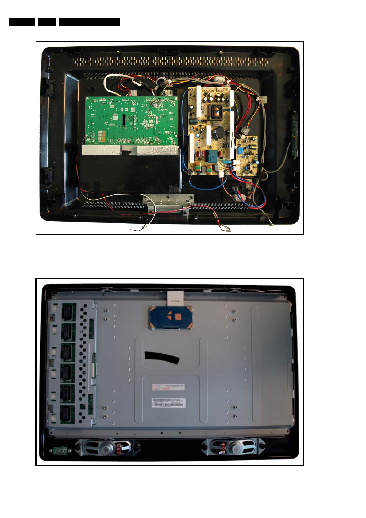
Figure 4-1 Cable dressing (20" model)
I_17930_064.eps
240408
Page 8
EN 8 TCM1.0E LA4.
Mechanical Instructions
Figure 4-2 Cable dressing (26" model) [1/2]
I_17930_046.eps
240408
Figure 4-3 Cable dressing (26" model) [2/2]
I_17930_044.eps
240408
Page 9
4.2 Service Positions
For easy servicing of this set, there are a few possibilities
created:
• The buffers from the packaging.
• Foam bars (created for Service).
Mechanical Instructions
EN 9TCM1.0E LA 4.
4.2.1 Foam Bars
Required for sets
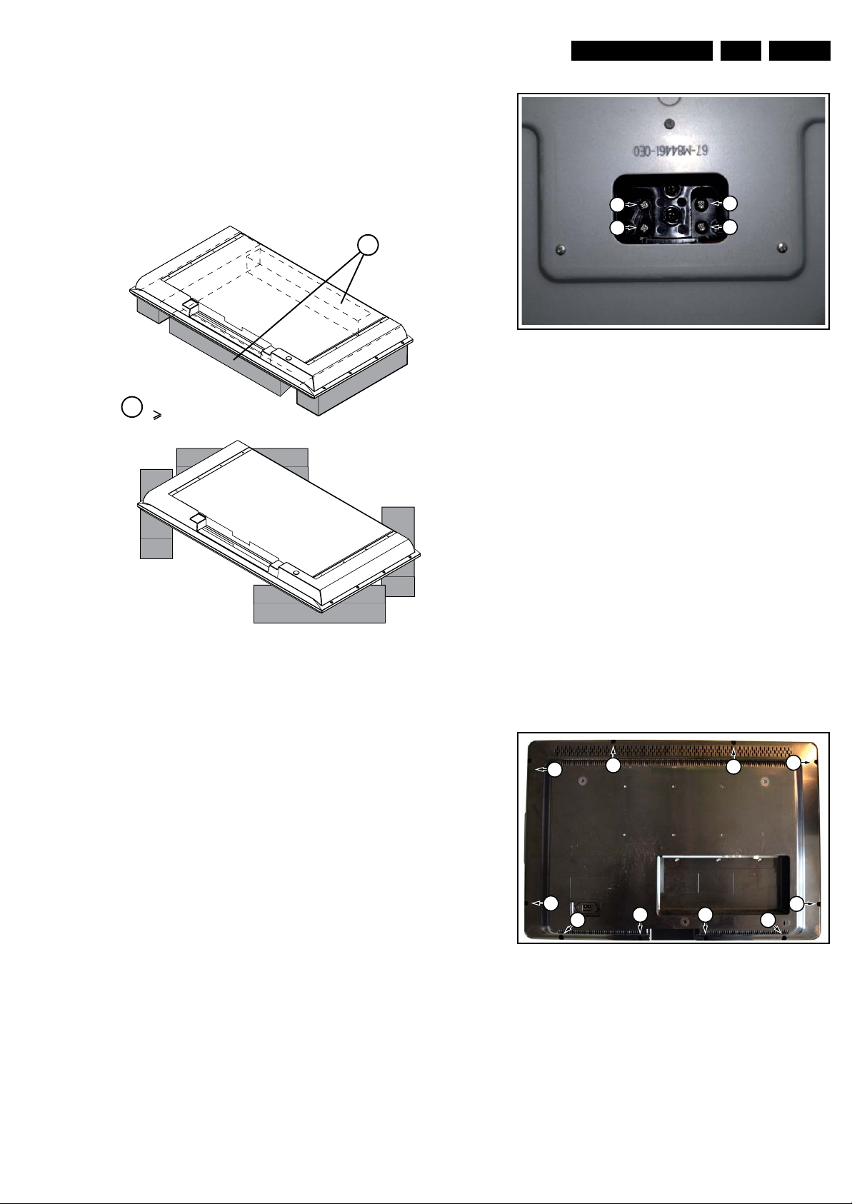
1
42"
Figure 4-4 Foam bars
The foam bars (order code 3122 785 90580 for two pieces) can
be used for all types and sizes of Flat TVs. See figure “Foam
bars” for details. Sets with a display of 42” and larger, require
four foam bars [1]. Ensure that the foam bars are always
supporting the cabinet and never only the display.
Caution: Failure to follow these guidelines can seriously
damage the display!
By laying the TV face down on the (ESD protective) foam bars,
a stable situation is created to perform measurements and
alignments. By placing a mirror under the TV, you can monitor
the screen.
1
E_06532_018.eps
171106
1
1
Figure 4-5 Stand
4.3.2 Rear Cover
Warning: Disconnect the mains power cord before you remove
the rear cover.
1. Refer to next figures.
2. Place the TV set upside down on a table top, using the
foam bars (see section “Service Positions”).
3. Remove the screws [1] that secure the rear cover. The
screws are located at the sides.
Be careful: Now the rear cover could be lifted but the SSB
and power supply panel(s) are mounted in the rear cover
and still connected to the LCD panel and other boards.
Those cables should be released first.
4. To release the LVDS cable lift the back cover a few
centimetres and move it downwards the set. Now unplug
the LVDS connector [2].
Caution: be careful, as this is a very fragile connector!
5. Remove the screw [3].
6. Now the rear cover can be lifted to gain access to the
speaker cables and the IR/LED panel cable. Release the
connectors [4].
1
1
1
1
1
I_17930_040.eps
240408
1
4.3 Assy/Panel Removal
4.3.1 Stand
1. Refer to next figure.
2. Place the TV set upside down on a table top, using the
foam bars (see section “Service Position”).
3. Remove the screws that secure the stand and remove the
stand.
1
1 1
Figure 4-6 Rear cover
11
1
I_17930_039.eps
240408
Page 10
EN 10 TCM1.0E LA4.
Mechanical Instructions
4.3.3 Keyboard Control Board
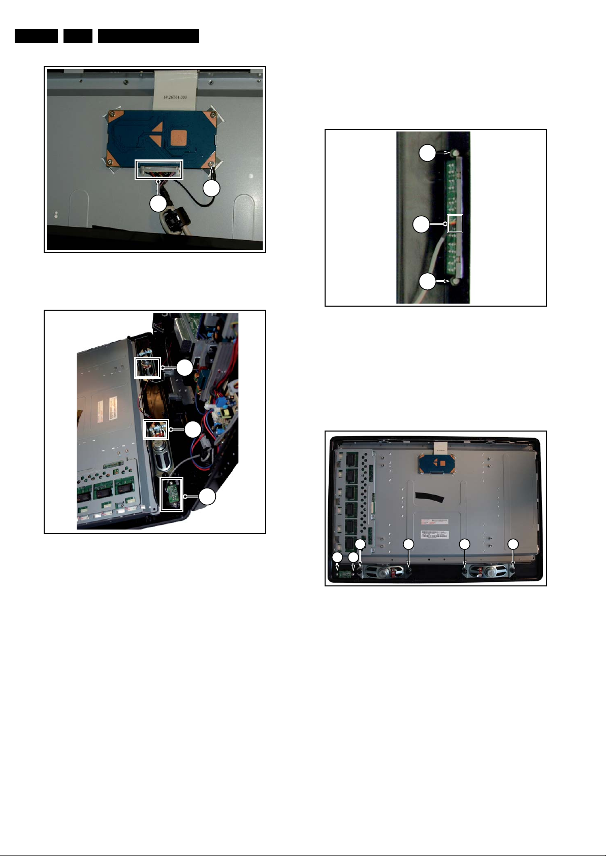
1. Refer to next figure.
2. Unscrew two screws[1]
3. Unplug connector [2] and remove the board.
When defective, replace the whole unit
1
3
2
2
I_17930_041.eps
240408
Figure 4-7 LVDS release
4
4
4
I_17930_042.eps
Figure 4-8 Speaker and IR/LED panel cable release
240408
1
Figure 4-9 Keyboard control board
4.3.4 IR/LED Board and Speakers
1. Refer to next figure.
2. Remove the screws [1] and remove the IR/LED board.
3. Remove the screws [2] and remove the speakers.
When defective, replace the whole unit.
22 22
1 1
I_17930_063.eps
240408
Figure 4-10 IR/LED Board and Speakers
I_17930_043.eps
240408
Page 11
Mechanical Instructions
EN 11TCM1.0E LA 4.
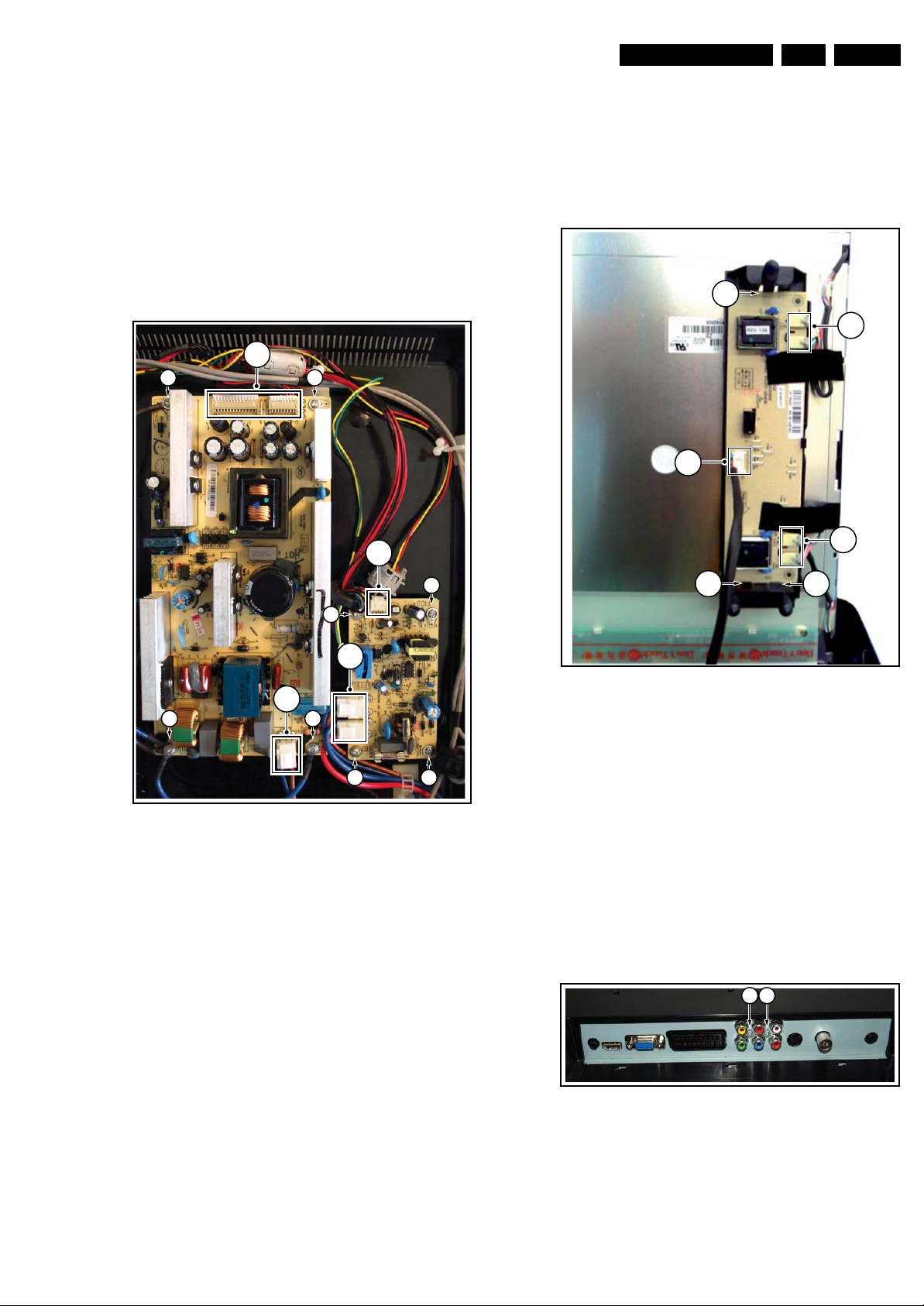
4.3.5 Power Supply Board
Due to different set executions this chassis is supplied with one
or two power supply boards and figures may differ.
Caution: it is absolutely mandatory to remount all different
screws and cables at their original position during re-assembly.
Failure to do so may result in damaging the power supply.
1. Refer to next figure.
2. Unplug all the connectors [1].
3. Remove the fixation screws [2]
4. Remove the main power supply board.
5. Unplug all the connectors [3].
6. Remove the fixation screws [4]
7. Remove the stand-by power supply board.
1
22
4.3.6 Inverter Board (19", 20" and 22" versions)
Due to different set executions this chassis some versions are
supplied with an inverter board. Figures may differ.
1. Refer to next figure.
2. Unplug all connectors [1].
3. Release the clips [2]
4. Take out the inverter board.
2
1
1
1
3
4
3
1
22
4 4
Figure 4-11 Power Supply Unit(s)
4
I_17930_045.eps
240408
2
Figure 4-12 Inverter Board
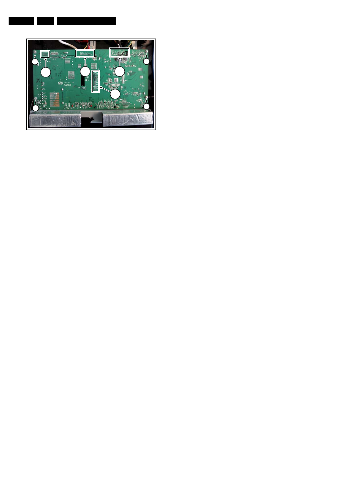
4.3.7 Small Signal Board (SSB)
Caution: it is absolutely mandatory to remount all different
screws at their original position during re-assembly. Failure to
do so may result in damaging the SSB.
Removing the SSB
1. See next figures.
2. Remove the screws [1] from the SSB connector plate.
3. Remove the screws [2] from the SSB.
4. Gently lift the board from the rear cover.
5. Now unplug the LVDS connector [3].
Caution: be careful, as this is a very fragile connector!
Unplug the rest of the cables [4].
1 1
2
I_17930_065.eps
240408
Figure 4-13 SSB connector plate
I_17930_047.eps
240408
Page 12
EN 12 TCM1.0E LA4.
s
8
Mechanical Instructions
2
4
4
3
2
Figure 4-14 SSB
4.4 Set Re-assembly
To re-assemble the whole set, execute all processes in reverse
order.
Notes:
• While re-assembling, make sure that all cables are placed
and connected in their original position. See figure “Cable
dressing”.
• Pay special attention not to damage the EMC foams at the
SB shields. Make sure, that EMC foams are put correctly
on their places.
4
I_17930_048.ep
2
2
24040
Page 13
Service Modes, Error Codes, and Fault Finding
5. Service Modes, Error Codes, and Fault Finding
Index of this chapter:
5.1 Test Points
5.2 Service Mode
5.3 Error Codes
5.5 Software Upgrading
5.1 Test Points
This chassis is NOT equipped with test points in the service
printing. These test points are NOT specifically mentioned in
the service manual.
5.2 Service Mode
5.2.1 Factory Mode or Service Alignment Mode (SAM)
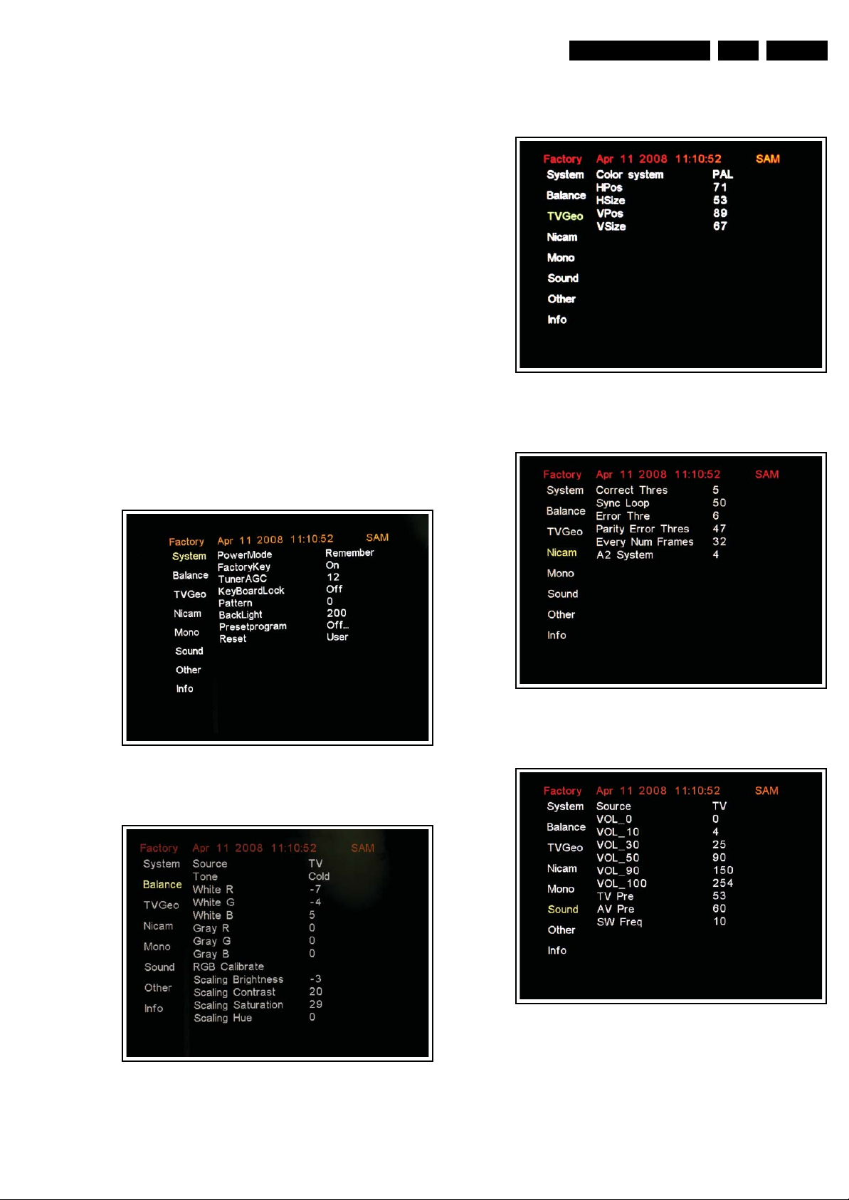
EN 13TCM1.0E LA 5.
How to Enter
To enter the Factory mode, use the following method:
• Press on the remote control the code “062596” directly
followed by the “INFO” key.
After entering the Factory mode, the following screen is visible,
the values can be adjusted according to the requested (see
Chapter 8).
I_17930_055.eps
240408
Figure 5-1 Factory mode menu, System
Figure 5-3 Factory mode menu, TV Geometry
Figure 5-4 Factory mode menu, Nicam
I_17930_057.eps
240408
I_17930_058.eps
240408
Figure 5-2 Factory mode menu, Balance
I_17930_056.eps
240408
Figure 5-5 Factory mode menu, Mono
I_17930_059.eps
240408
Page 14

EN 14 TCM1.0E LA5.
Service Modes, Error Codes, and Fault Finding
5.2.2 Customer Service Mode (CSM)
Purpose
When a customer is having problems with his TV-set, he can
call his dealer or the Customer Help desk. The service
technician can then ask the customer to activate the CSM, in
order to identify the status of the set. Now, the service
technician can judge the severity of the complaint. In many
cases, he can advise the customer how to solve the problem,
or he can decide if it is necessary to visit the customer. The
CSM is a read only mode; therefore, modifications in this mode
are not possible.
How to Activate CSM
Key in the code “123654” via the standard RC transmitter.
Figure 5-6 Factory mode menu, Sound
Figure 5-7 Factory mode menu, Other
I_17930_060.eps
240408
I_17930_061.eps
240408
Contents of CSM
Figure 5-9 CSM Menu
I_17930_062.eps
240408
I_17930_061.eps
240408
Figure 5-8 Factory mode menu, Info
How to EXIT
Choose “EXIT”, then press the “MENU” button on the remote
control.
Page 15
Service Modes, Error Codes, and Fault Finding
EN 15TCM1.0E LA 5.
Menu Explanation
1. Set Type Type number and region.
2. Production code Product serial no.
3. SW naming main-processor Software cluster and version
is displayed.
4. Standby MCU SW Software version stand-by μProcessor.
5. Code Error buffer contents.
6. NVM NVM version.
7. Signal Quality Yes/No (antenna signal).
8. System TV system (PAL)
9. Sound Audio system (Mono/Stereo/Nicam stereo)
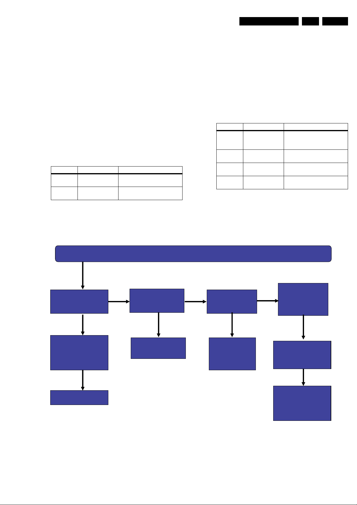
5.3 Error Codes
The error code buffer contains all errors detected since the last
time the buffer was erased. The buffer is written from left to
right. When an error occurs that is not yet in the error code
buffer, it is displayed at the left side and all other errors shift one
position to the right.
Basically there are six kind of errors:
Error code Area Description
2 MT8293 Communication error with
MT8293
3 μP Control Communication error with
standby MCU
10. Key (HDCP) HDMI Shows Valid or invalid when HDMI
connected. Else blank.
11. HDMI input format Shows HDMI picture format display,
i.e. 480p30, when HDMI connected. Else blank.
12. HDMI audio Stream Show Yes/No when HDMI connected.
Else blank.
How to exit
Press “MENU” on the RC-transmitter.
Error code Area Description
4 IIC bus Error Communication error on I2C
6 System EEPROM
(NVM)
7 Tuner Communication error with
8 Demodulator Communication error with
bus (none of the I
respond)
Communication error with
system EEPROM
tuner.
demodulator.
2
C devices
5.4 Fault Finding
No Picture, no sound, no Black light, Fuse Broken
Pin2~3 is 5v&Pin
8~11 is 12V of
P502 OK?
Check Pin7~8 of
P503 & pin8~9 of
J8
Check PSU
NO
Y
pin4~5 is 5V &
pin7~8 is12V of
SEYSE
Is U1-U5, U11
OK?
YES
U505 OK?
ONON
Check Pin 4 Of
UM01 is 3.3v
Replace Bad
NO
one of
u1~u5,u11
Check
LQPF jointing of
U6
YES
Check Y1,C23,C69
& IIC Bus &Reset
YES
Check jointing of
U8,u7,R213~R218,
R42,R44.
Figure 5-10 No Picture, no sound, noBlack light, Fuse Broken
I_17930_076.eps
250408
Page 16
EN 16 TCM1.0E LA5.
Service Modes, Error Codes, and Fault Finding
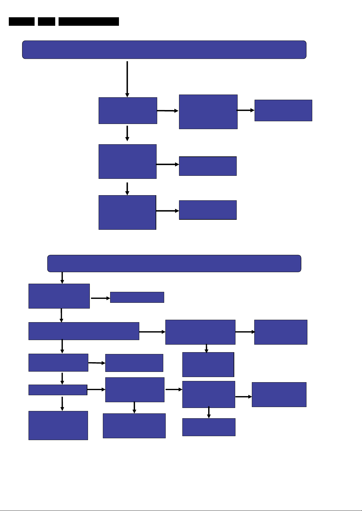
No Picture, Black light & Sound OK
Check output
volt of u20 is
OK?
No
Cap of p504 is
better & C of
Q12 is low volt.
Yes
Check
waveform of
L201~L212 is
OK?
Yes
check the
cable to panel
No
Is
Pin207,216,225
of u6 shorted to
No
check pin
208~239 of u6
earth?
Figure 5-11 No Picture, Black light & Sound OK
Picture OK, No sound
Check
Yes
Replace U20
I_17930_077.eps
250408
Check 12v
Pin 3,13 of u001
OK?
Yes
Check stby
Pin 7 & Mute Pin6 of U001 OK?
Yes
Check audio DAC
R & L of u002 OK?
No
TV source
Yes
Check IF circuit
or Replace
U601
No
Yes
No
Check u505
NO
Check
R & L speaker
Check audio
ADC
R & L of u003 OK?
Yes
check pin31,32,35
of u6 or Replace
u002
Figure 5-12 Picture OK, No sound
Check C of Q002 is
5V,B of Q002 is Low
OK?
Yes
Check
Pin 7 of U001 is
6V
No
Check audio
Switch R&L of
U16 OK?
No
check u16
or Replace u16
No
Yes
Change the
component
pin31,32,33 of u6
or replace u003
damage
Check
I_17930_078.eps
250408
Page 17

Service Modes, Error Codes, and Fault Finding
No colour
EN 17TCM1.0E LA 5.
Colour
system is
Yes
Dose the TV
signal too
Right?
No
Reset
To
Local system
5.5 Software Upgrading
5.5.1 ComPair
Introduction
ComPair (Computer Aided Repair) is a Service tool for Philips
Consumer Electronics products. and offers the following:
1. ComPair helps you to quickly get an understanding on how
to repair the chassis in a short and effective way.
2. ComPair allows very detailed diagnostics and is therefore
capable of accurately indicating problem areas. You do not
have to know anything about I
yourself, because ComPair takes care of this.
3. ComPair speeds up the repair time since it can
automatically communicate with the chassis (when the uP
is working) and all repair information is directly available.
4. ComPair features TV software upgrade possibilities.
Specifications
ComPair consists of a Windows based fault finding program
and an interface box between PC and the (defective) product.
The (new) ComPair II interface box is connected to the PC via
an USB cable. For the TV chassis, the ComPair interface box
and the TV communicate via a bi-directional cable via the
service connector(s).
How to Connect
This is described in the ComPair chassis fault finding database.
Tuner Input
cable & antenna
2
C or UART commands
weak?
YES
Check
NO
Figure 5-13 No colour
Check
Pin 17 of
U601 OK?
NO
Check
U601
YES
Check
U6
I_17930_079.eps
250408
TO TV
TO
UART SERVICE
I2C SERVICE
CONNECTOR
CONNECTOR
2
C
I
PC
ComPair II Developed by Philips Brugge
Optional power
5V DC
TO
RS232 /UART
E_06532_036.eps
150208
TO
UART SERVICE
CONNECTOR
ComPair II
RC in
Optional
Switch
Power ModeLink/
Activity
HDMI
I
2
C only
RC out
Multi
function
Figure 5-14 ComPair II interface connection
Caution: It is compulsory to connect the TV to the PC as
shown in the picture above (with the ComPair interface in
between), as the ComPair interface acts as a level shifter. If
one connects the TV directly to the PC (via UART), ICs will be
blown!
How to Order
ComPair II order codes:
• ComPair II interface: 3122 785 91020.
• For SW see Philips service website.
• ComPair/UART interconnection cable: 3122 785 90630.
• ComPair/UART adapter cable: 3122 785 91070.
Note: If you encounter any problems, contact your local
support desk.
5.5.2 LVDS Tool
Support of the LVDS Tool has been discontinued.
Page 18

EN 18 TCM1.0E LA5.
Personal Notes:
Service Modes, Error Codes, and Fault Finding
E_06532_012.eps
131004
Page 19
Block Diagrams, Test Point Overview, and Waveforms
6. Block Diagrams, Test Point Overview, and Waveforms
Wiring diagram not available at time of publishing.
For wiring see chapter 4 figure: cable dressing.
19TCM1.0E LA 6.
Page 20
Block Diagrams, Test Point Overview, and Waveforms
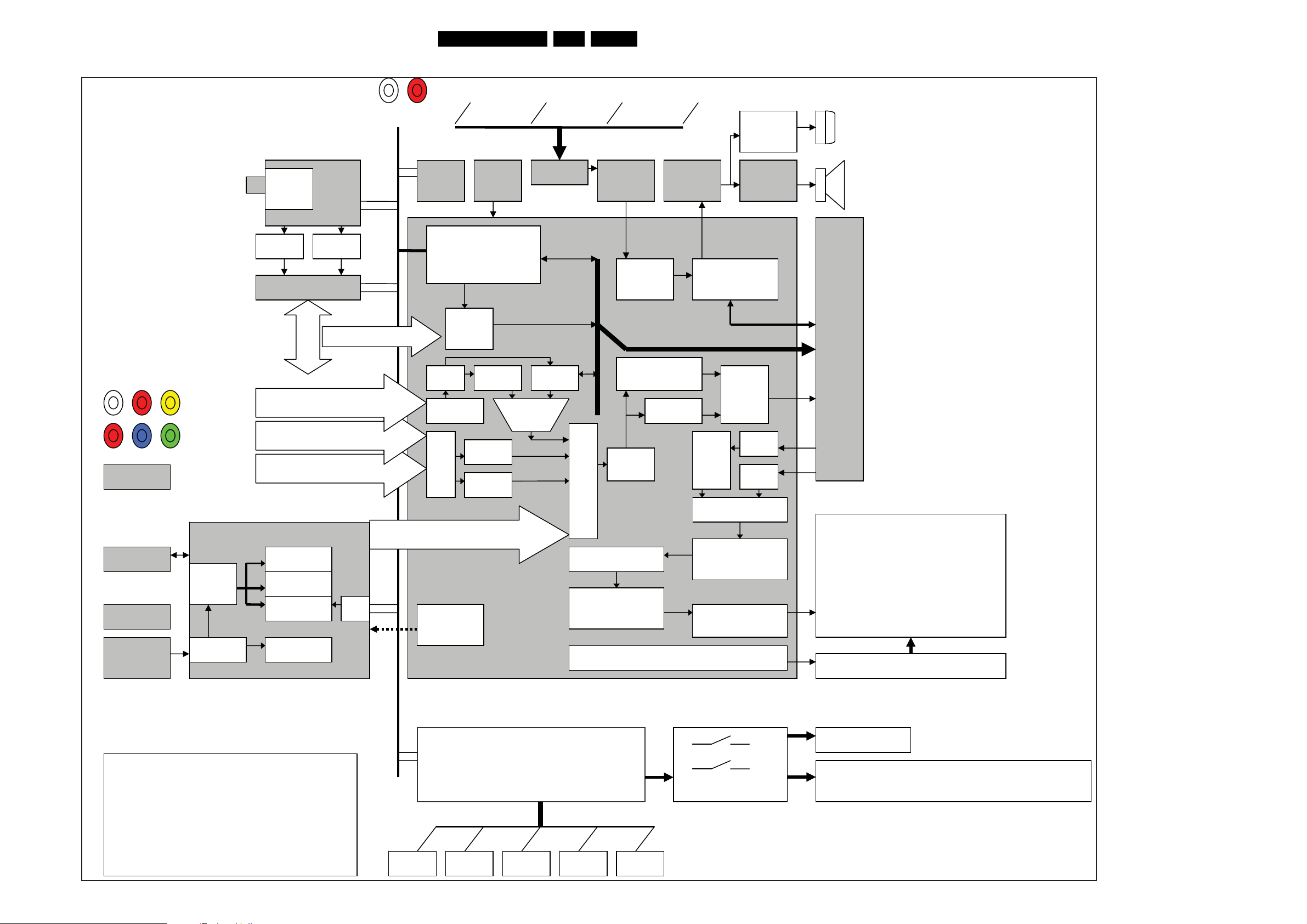
Block Diagram MT8200
20TCM1.0E LA 6.
MT00 BLOCK DIAGRAM MT8200
Tuner
Tuner
D9453D
TDA9886T
TV/AV/SCART CVBS
YUV/RGB
VGA
VGA EDID
D3953N
VBI decode
I2C
Av audio
E2P
ROM
TVD
ADC x 8
A
D
C
MCU
8032
VBI
Slicer
FLASH
2MB
HDTV
VGA D
Scart Audio
YUV
D
HEF4052
3DComb2DComb
M
U
X
PC Audio
ADC
WM8783
Demodulator
De-interlacing
Shrink
Side Av audio
Sound
Bypass
DAC
WM8501
Color
Proce
ssing
Driver
AMP
TDA
7266
DSP
Audio Processing
DoSc
UpSc
Osd
Earphone
Speaker
DRAM
8MX16
HDCP
HDCP
Engine
HDMI EDID
CM2021
HDMI ESD
Configure On MT00 Classis:
1, TV/ VGA/ YPBPR/ HDMI&HDCP/ SCART / AV&SIDE AV/ YC…VIDEO IN
2, SCART CVBS OUT …………………………………..………………VIDEO OUT
3, TV/ VGA/HDMI&HDCP/ SCART / YPBPR&AV& YC/ SIDE AV…AUDIO IN
4, BTL OUT/EARPHONE OUT..………………………………………..AUDIO OUT
5, LVDS(single/double)/TTL…………………………………………..SIGNAL OUT
6, INVERTER CON/KEY&IR CON/SIDE AV&EARPHONE/UART…INTERFACE
7, TELETEXE/NICAM/German Stereo………………………………..
8, STANDBY MODE BLOW .3W……………………………………….STANDBY
9, DC TO DC(12V TO 5V) FOR 26”……………………………………DC TO DC
10, MT8200/SDRAM/FLASH/MT8293/KA9222/TDA9886/
RESET/ADC/DAC/AUDIO SWITCH/EEPROM………………..….IC
MTDS Core
Video Process
Audio Decoder
Mode Control
Detect
MT8200A*E
Mixer
HDMI
Gamma
R/G/B LTI
GAIN/OFFSET
LCD PANEL
2
c
I
Clock
27M Hz
out
POWER SUPLLY CONTROL MCU
KA-9222
IR LED r
LED g
Output masking
Dithering
LV D S/TTL TX
Back light /PWM Brightness control
12V P_
5V VCC
Dual P-Channel
MOSFET
KEY
POWER
AMP
INVERTER
TDA7266
LDO (U1:LD1084,U3: LD1084,U5: ld1117) VCC to 3V3;
LDO (U2:LD1084,U4: LD1084,U11: ld1117) 3V3 to 1V8
I_17930_038.eps
220408
Page 21
Circuit Diagrams and PWB Layouts
7. Circuit Diagrams and PWB Layouts
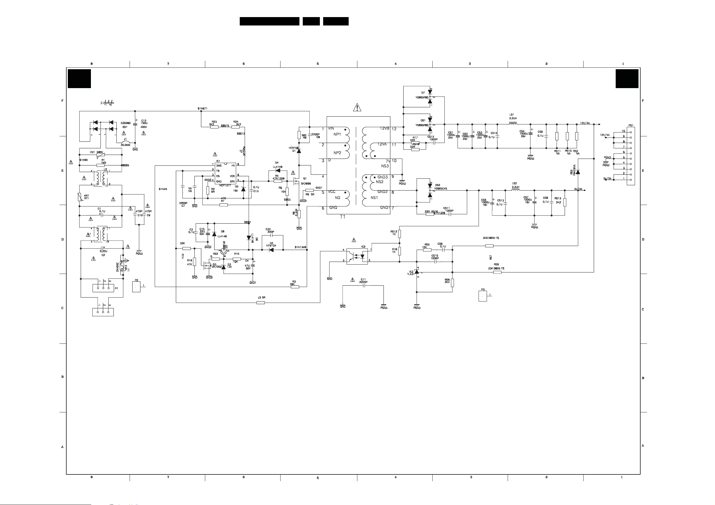
Main Power Supply (19" & 20")
21TCM1.0E LA 7.
A A
MAIN POWER SUPPLY 19” & 20”
I_17930_024.eps
220408
Page 22
Circuit Diagrams and PWB Layouts
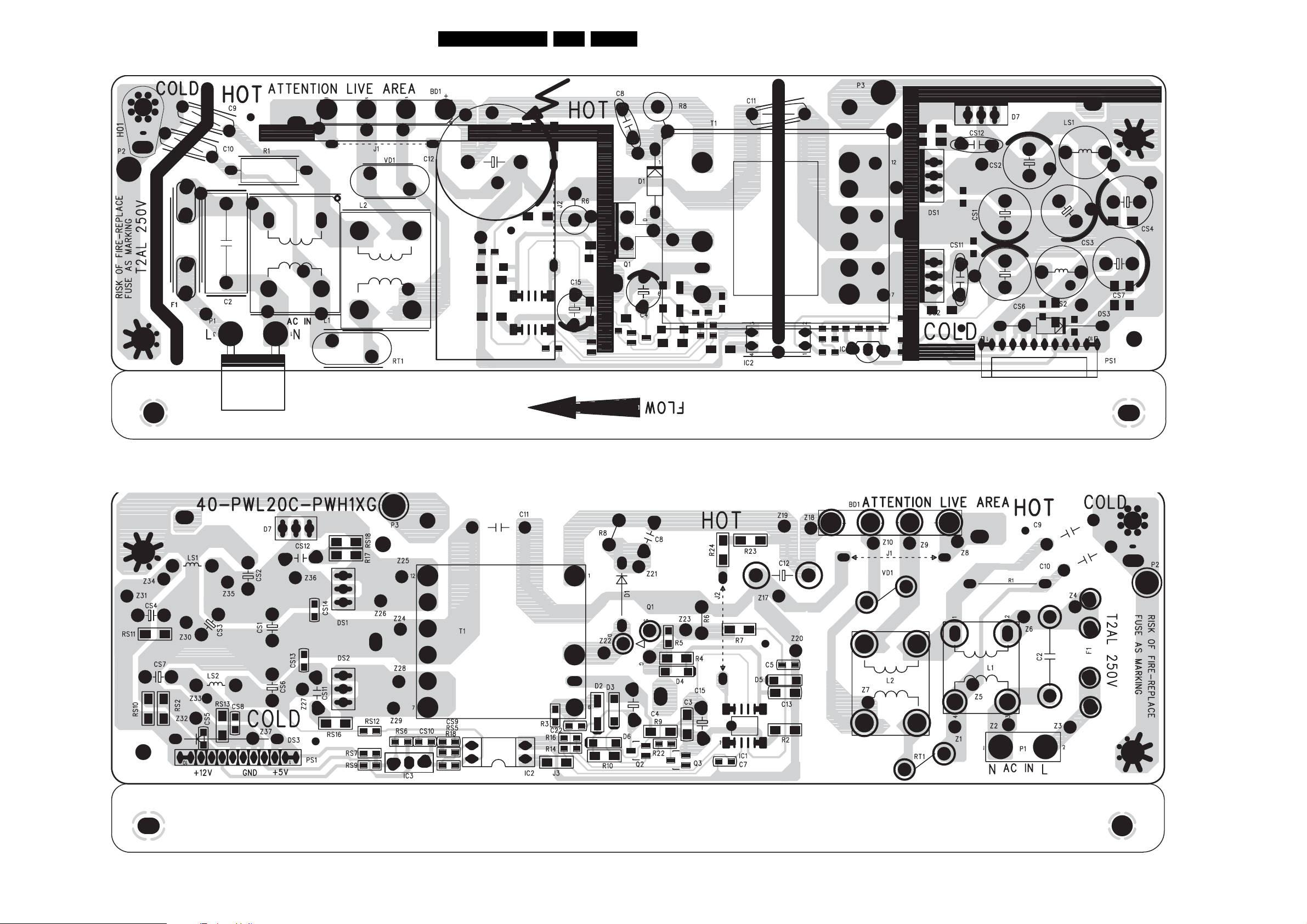
Layout Main Power Supply (20") (Top Side)
22TCM1.0E LA 7.
Layout Main Power Supply (20") (Bottom Side)
I_17930_025.eps
220408
I_17930_026.eps
220408
Page 23
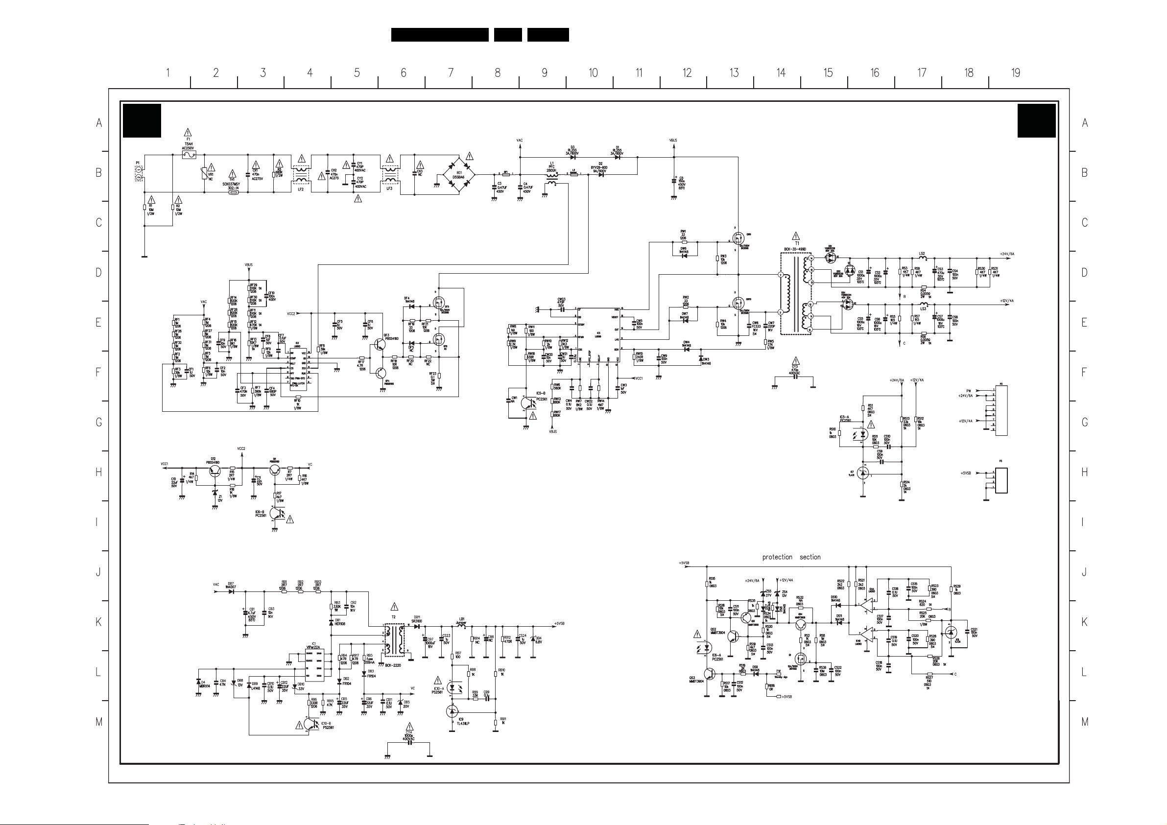
Main Power Supply (26")
Circuit Diagrams and PWB Layouts
23TCM1.0E LA 7.
A1 A1
MAIN POWER SUPPLY 26”
I_17930_027.eps
220408
Page 24
Circuit Diagrams and PWB Layouts
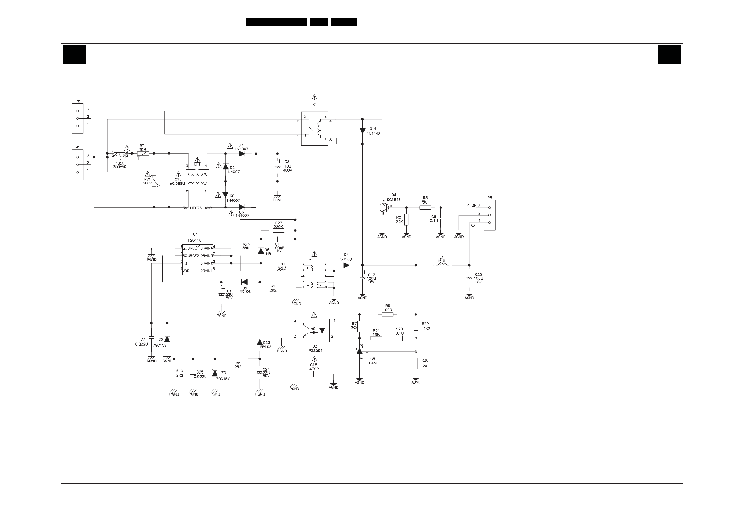
Standby Power Supply (26")
24TCM1.0E LA 7.
A2 A2
STANDBY POWER SUPPLY 26”
I_17930_028.eps
220408
Page 25
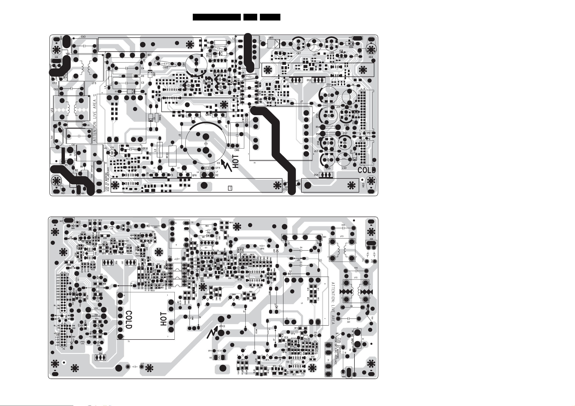
Circuit Diagrams and PWB Layouts
Layout Main Power Supply (26") (Top Side)
25TCM1.0E LA 7.
Layout Main Power Supply (26") (Bottom Side)
I_17930_029.eps
220408
I_17930_030.eps
220408
Page 26
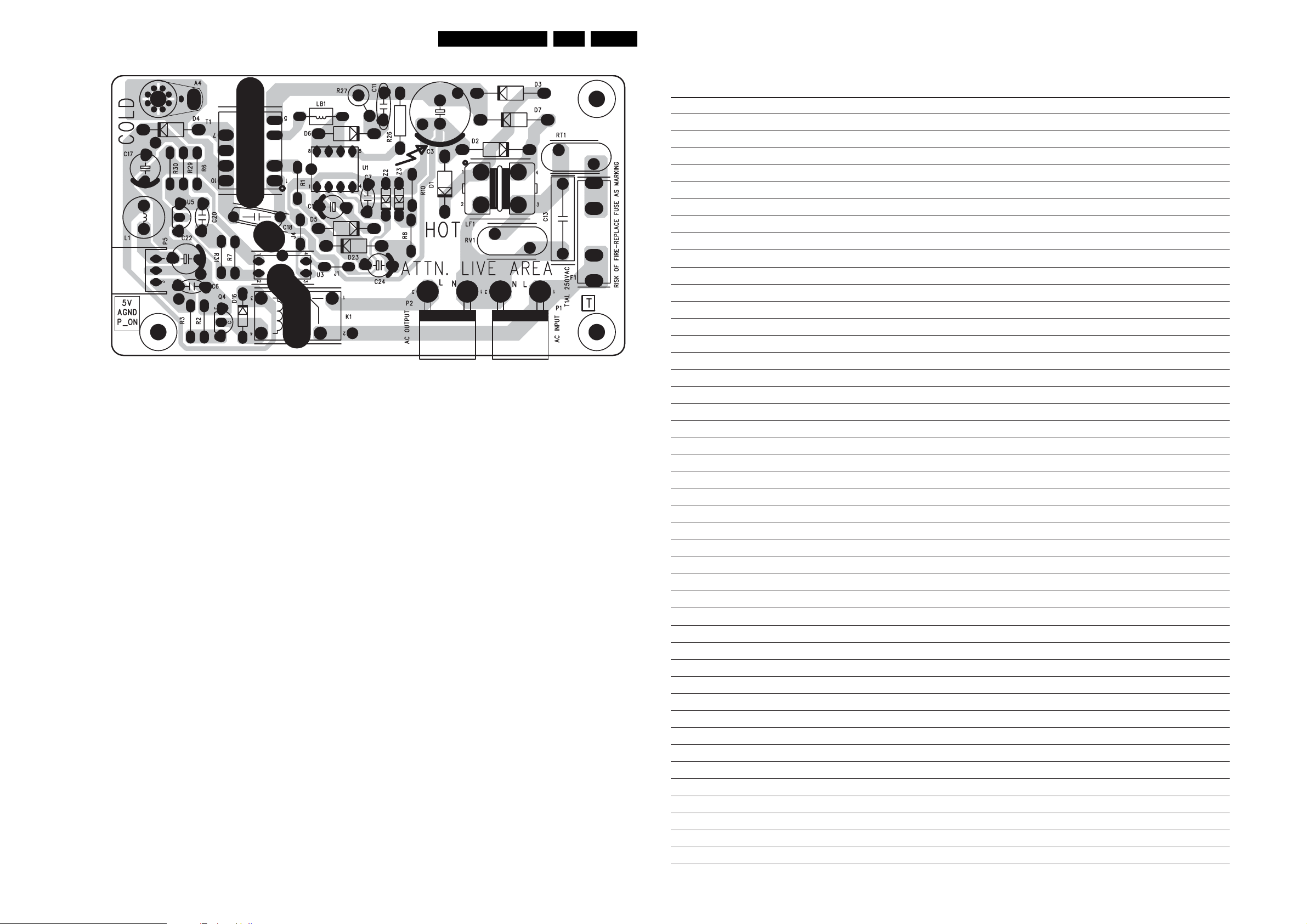
Circuit Diagrams and PWB Layouts
Layout Standby Power Supply (26") (Top Side)
26TCM1.0E LA 7.
Personal Notes:
I_17930_075.eps
250408
E_06532_012.eps
131004
Page 27
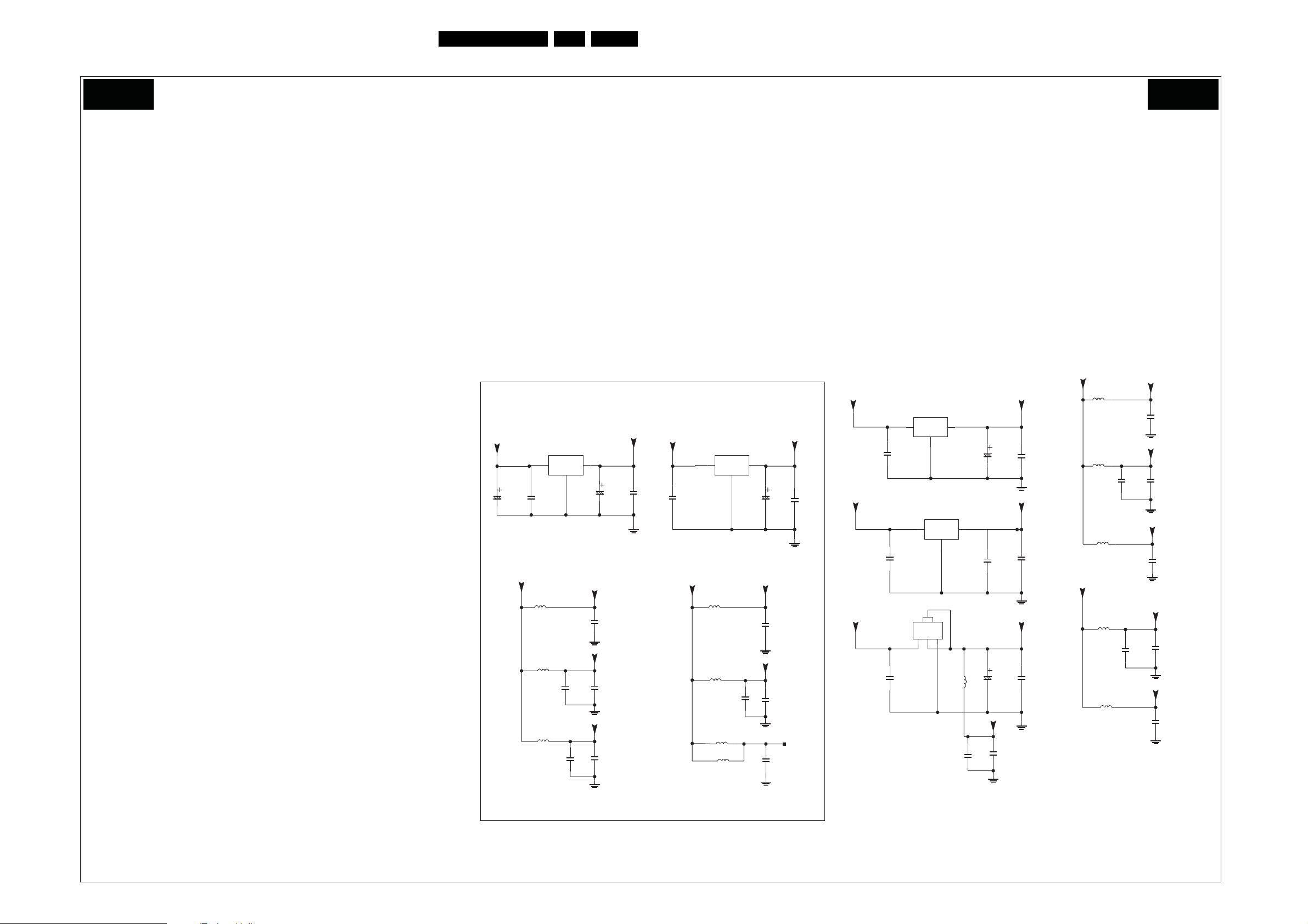
Circuit Diagrams and PWB Layouts
SSB: Index /GPIO List /LDO
27TCM1.0E LA 7.
B01 B01
INDEX /GPIO LIST /LDO
MT8200_SZ_V1
1. INDEX /GPIO LIST /LDO
2. MT8200 LQFP256
3. DDR MEMORY & FLASH
4. VGA INPUT
5. INTERFACE FOR LVDS\ TTL\ KEY BOARD\ RS-232
6. TUNER BLOCK
7. SCART INPUT INTERFACE
8. AV & S_VIDEO & PC-AUDIO INPUT
9. AUDIO SWITCH & AUDIO POWER AMPLIFER & EARPHONE INTERFACE
10. HDMI BLOCK
11. POWER SUPPLY& MUC FOR STANDBY & INVERTER
GPIO LIST
I2C LVDS---SDA:ERO1;SCL:ERO0
TTL---SDA:GPIO10;SCL:F_A21
WRITE ENABLE FOR EEPROM:GPIO8
UPDATE BY VGA:DQ17
LV DS POWER:GPIO9
GPIO_PANEL:GPIO/TXD
KEY:ADIN1
LED:FCICLK
POWER_STBY:UP3_4
BL ON/OFF: PWM1
TIMING:PWM0
SWITCH 4052 :SCL0 SDA0 11-AV1;01-PC;00-AV3
SW_MUTE:DQ23
USB_IR_INPUT:DQ20
GPIO_DVB1:GPIO/RXD
16V
Schematic For MT01(8200) Chassis
VCC
220U
CE6
SB33
SB33
U1
AIC1084
23
VOUTVIN
ADJ/GND
1
0.1U
C67
L4
200R
L9
200R
1U
C907
L12
200R
1U
C908
6V3
SB33B
0.1U
CB13
SB33A
0.1U
CB19
ASB33A
CB22
0.1U
C901
47U
0.1U
CB5
SB33A
CB6
0.1U
SB18
KD1084AD2T18
L5
200R
L8
200R
L60
200R
L61
200R
U2
ADJ/GND
V33
L6
V33VCC
U3
LD1086
23
OUTIN
U5
LD1117S33
ADJ/GND
1
U4
LD1086
23
OUTIN
ADJ/GND
1
4
4
GND/ADJ
OUT
VIN
123
1U
C906
L13
1000UR
6V3
C904
6V3
1U
SDV33
C903
47U
0.1U
CB9
V18
0.1U
CB11
DV33B
C905
47U
0.1U
CB17
E
CB203
0.1U
SB18
V33
VCC
C37
0.1U
CB10
CB16
0.1U
0.1U
23
OUTVIN
1
1U
C909
B
16V
SB18A
0.1U
ASB18A
CB18
0.1U
C197
220U
0.1U
DV18A
CE1
CB12
0.1U
CB8
200R
L10
200R
L100
200R
V18
L7
200R
L11
200R
C910
1U
C911
AV33A
0.1U
CB14
ADCV33A
0.1U
CB20
DV33A
0.1U
CB24
ADCV18A
0.1U
CB15
1U
AV18A
0.1U
CB21
I_17930_011.eps
220408
Page 28
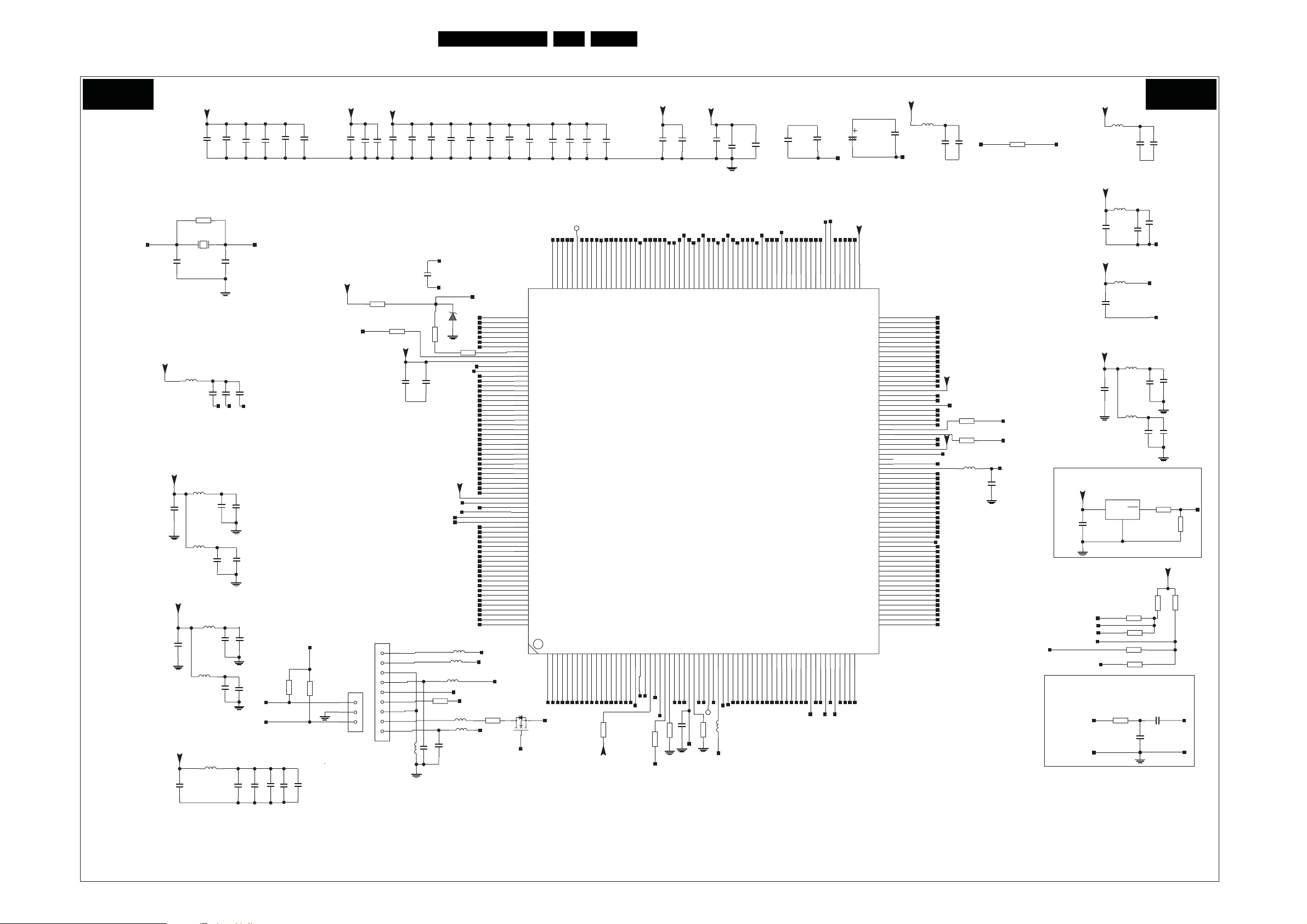
SSB: MT8200 LQFP256
Circuit Diagrams and PWB Layouts
28TCM1.0E LA 7.
B02 B02
DV18A
0.1U
CB47
A B C D
CB51
CB50
0.1U
3300P
3300P
CB49
3300P
CB48
0.1U
CB52
DV33A
CB57
0.1U
CB61
0.1U
Near the MT8201
CB63
0.01U
CB62
0.1U
0.01U
CB64
0.01U
CB65
CB66
0.1U
CB69 0.01U
0.01U
0.01U
0.01U
C89
C103
0.01U
C87
C86
SDV33
CB60
0.1U
0.1U
0.1U
CB59
CB58
SB18A
CB70
0.1U
CB71 0.01U
SB33A
0.1U
NORMAL ANALOG POWER
CB67
CB68
3300P
0.01U
CB73
0.1U
CB32
AVICM PWM2VREF
CE35
6V3
47U
1U
CB204
GND
MT8200 LQFP256
AV18A
VPLLVDD1
L17
200R
0.1U
C68
GND
1U
C10
CB30
GND
0.1U
TESTN4 VPLLVDD1
R15
49R9/NC
E
AV33A
L19
120R
D
VPLLVDD2
1U
0.1U
C15
CB33
GND
ASB18A
R18
820K
Y1
XTALI XTALO
27M
22P
C23
27P
C69
AV33A
L20
120R
C20
0.1U
LVD D
0.1U
0.1U
GND GND
GND
CB38
CB40
ADCV33A
L24
AADCVDD
200R
0.1U
C38
1U
0.1U
CE40
CB42
L26
200R
ADACVDD
1U
0.1U
CB46
CE42
ADCV33A
FB2
120R
AVDD_VFE0
1U
0.1U
C17
120R
AVDD_VAD0
1U
C19
CB35
0.1U
CB39
0.1U
CB37
FB3
A
ASB18A
FB1
200R
TXD
RXD
R45
10K
PLLVDD
RS232
5VSB
R46
10K
RS-232
TXD
GND
RXD
5VSB
5VSB
1
2
3
R600
270R
ADCIN0
1K
R65
ADCVDD
1U
C25
KEY BOARD
KEYPAD INTERFACE
J8
5VSBIN
9
8
GND
7
6
KEY
5
ON_LED
4
SB_LED
3
GND
2
IR
1
J3
5VSB
CB205
C39
GND
5VSBOUT
600R
L41
0.1U
0.1U
C40
R602
0.1U
5VSBIN
CB201
XTALVDD
GND
3K3
KEY2
R163
0.1U
D15
L43
10K
MADV33
3V3
SB18A
L66
NC/600
L59
600R
600R
LED
LEDR
L44
600R
L67
R78
10K
IR_INPUT
600
5VSB
5VSB
5VSB
KEY2
ERO1
ERO0
SB18A
GND
PLLVDD
GND
PLLVDD
XTALVDD
XTALO
XTALI
ADCVDD
PWM2VREF
TESTN4
VPLLVDD1
VPLLVDD2
LVD D
AP7
AN7
CLK2+
CLK2AP6
AN6
AP5
AN5
LVD D
AP4
AN4
AP3
AN3
CLK1+
CLK1AP2
AN2
LVD D
AP1
AN1
AP0
AN0
SB18A
ERO3
SB33A
ERO2
VSYNCO
HSYNCO
DE
VCLK
F_A17
F_A0
F_D7
F_D6
F_D5
F_D4
F_D3
F_D2
F_D1
F_D0
F_OE#
IOCE#
F_A1
F_A16
F_A15
F_A14
R105
L16
SCART_FB
137
FAST_BLANK
DVDD2_7
SCL0
136
SCL0/GPIO
DQS1
SDA0
135
SDA0/GPIO
DQ8
HDMILRCK
HDMISD0
133
134
HDMISD0
HDMILRCK
RVREF
DQ9
DV33A
DV18A
HDMIMCLK
HDMIBCLK
130
132
131
DVDD1 8_3
HDMIBCLK
HDMIMCLK
DQ11
DQ10
DQ12
63
64
DV33A
129
DVDD33_1
VCLK_DVI
DVDD18_2
DE_DVI
HSYNC_DVI
VSYNC_DVI
DE_SOG
OUT_27MHZ
PWM1
PWM0
DVDD33
DQ30/GPIO
DVDD2_1
DQ28/GPIO
DQ24/GPIO
DVDD2_2
DQ23/GPIO
DQ20/GPIO
DVDD18_1
DVDD2
DQ17/GPIO
DVDD2_3
RCLKB
DVDD2_4
DVDD18_4
RWE_
DVDD2_5
RA11
RCLK
RA10
RCS_
RAS_
CAS_
DQ15
DQ14
DQ13
0.1U
C4
ASB33A
L18
0.1U
VI15
VI14
VI13
VI12
VI11
VI10
VI9
VI8
VI7
VI6
VI5
VI4
VI3
VI2
VI1
VI0
RA4
RA5
RA6
RA7
RA8
RA9
CKE
RA3
RA2
RA1
RA0
BA1
BA0
VI14
127
VI13
126
VI12
125
VI11
124
VI10
123
VI9
122
VI8
121
VI7
120
VI6
119
VI5
118
VI4
117
HDMIODCK
116
115
114
113
112
111
DE_HDMI
110
109
108
107
106
105
104
103
102
101
100
99
98
97
96
95
94
93
92
91
90
89
88
87
86
85
84
83
82
81
80
79
78
77
76
75
74
73
72
71
70
69
68
67
66
65
VI3
VI2
DV18A
VI1
VI0
HSYNC_HDMI
VSYNC_HDMI
DE_SOG
27MHZ
DV33A
SDV33
DQ28
SDV33
DQ20
DV18A
SDV33
DQ17
A_RA4
A_RA5
A_RA6
A_RA7
A_RA8
A_RA9
A_RA11
A_CKE
SDV33
A_CLK
RCLKB1
A_RA3
A_RA2
A_RA1
A_RA0
A_RA10
SDV33
A_BA1
DV18A
A_BA0
A_CS#
A_RAS#
A_CAS#
A_WE#
A_DQ15
A_DQ14
A_DQ13
SDV33
DQ30
DV18A
SDV33
100R
100R
R14
PWM1
R13
PWM0
L58
600R
MUTE
C121
200P
RESET IC
I2C
VI15
128
F_A21
C11
ADCV18A
0.1U
CB43
VCC
C41
0.1U
GPIO10
SDA
ERO0
SCL
U100
ERO1
Z8
T
PB0N
Y1N
PR1N
SC0
SY0
PR1P
SY1
PB1N
SC1
MPX1
CVBS0
AVIC M
PLLVDD
TESTN3
TESTP3
190
191
192
TN3
PLLVSS2
PLLVDD2
PLLVSS3
PLLVDD3
XTALVDD
XTALO
XTALI
ADIN1/GPIO
ADIN0/GPIO
ADCVDD
PWM2VREF
TN4
VPLLVDD1
VPLLVDD2
LVD DA
A7P
A7N
CK2P
CK2N
A6P
A6N
A5P
A5N
LVD DB
A4P
A4N
A3P
A3N
CK1P
CK1N
A2P
A2N
LVD DC
A1P
A1N
A0P
A0N
DVDD1 8A
ERO3
DVDD33A1
ERO2
ERO1
ERO0
VSYNCO
HSYNCO
DE
VCLK
A17
IOA0
AD7
AD6
AD5
AD4
AD3
AD2
AD1
AD0
IOOE
IOCS
IOA1
DVDD1 8A1
A16
HIGHA7
HIGHA6
HIGHA5
1
2
PLLVDD1
HIGHA4
HIGHA3
495
193
194
195
196
197
198
199
200
201
202
203
204
205
206
207
208
209
210
211
212
213
214
215
216
217
218
219
220
221
222
223
224
225
226
227
228
229
230
231
232
233
234
235
236
237
238
239
240
241
242
243
244
245
246
247
248
249
250
251
252
253
254
255
256
GND
189
TP3
HIGHA2
ACENT
188
ADACVSS
HIGHA1
637
TESTP2
GND
ADACVDD
AR
AL
TESTN2
183
180
181
182
184
187
186
185
TP2
TN2
AVICM
ACENT
IOA20
AADCVSS
ADACVDD
AL/AOSDATA0
AR/AOSDATA1
HIGHA0
IOA19
IOA6
IOA18
IOA7
IOWR_
IOA21
8
13
101112
14
AVDD_VAD0
AADCVDD
178
179
SIF
AADCVDD
IOA4
IOA5
16
15
CVBS3
CVBS2
CVBS1
GND
GND
AVDD_VFE0
175
173
169
170
171
176
174
172
177
SY0
CVBS2
CVBS1
CVBS3
CVBS0
AVSS_VFE0
AVDD_VFE0
AVSS_VAD0
AVDD_VAD0
IOA2
DVDD33A
IOA3
17
UP3_4
WR_
RD_
INT0
PRST_
IOALE
21
20
18
19
222324
25
PB1P
AVDD_VAD1
163
164
165
166
168
162
161
167
SY1
SC1
SC0
PB1P
PB1N
PR1P
PR1N
AVDD_VAD1
MT8200
TXD
DVDD1 8
RXD
AOMCLK
IR
AOBCK
ICE
AOLRCK
26
27
282930
31
323334
Y0N
Y0P
PB0P
Y1P
PR0N
PR0P
SOY1
159
160
Y1P
Y1N
SOY0
158
153
155
154
152
157
156
Y0P
Y0N
PB0P
PR0P
PB0N
PR0N
SOY1
U6
DVDD18_5
GPIO/TXD
GPIO/RXD
GPIO8
AOSDATA3
AOSDATA1
LIN
35
36
FCICLK/GPIO
37
38
39
GPIO7
41
424344
40
SOY0
GPIO9
GND
151
TESTP1
150
VSS_VAD1
GPIO10
TESTN1
AVDD_VFE1
148
149
TP1
TN1
EXT_GND
DVDD33_2
454647
RP
RN
147
146
RN
AVDD_VFE1
DQ0
DQ1
48
GN
GP
BN
VGASOG
BP
GND
VGAHSYNC#
VGAVSYNC#
139
145
144
143
141
140
138
142
BP
BN
RP
GP
GN
SOG
VSYNC
HSYNC
AVSS_VFE1
DQ2
DQ6
DQ3
DQ5
DQS0
DVDD2_6
DQ4
DQ7
DQM0
51
52
535455
49
56575859606162
50
WR1
URST#
RD1
F_A11
F_A10
F_A9
F_A20
F_A21
IOWR#
F_A19
F_A18
F_A8
R21
SB33A
F_A7
4K7
F_A13
F_A12
Q7
2N7002
1K
IR
VCC
F_A6
F_A5
F_A4
ALE1
F_A2
F_A3
INT0#
SB33A
TXD
RXD
ICE
DOUT
AOLRCK
DV18A
AOBCLK
POWER_STBYC
12P
1K
R22
1K
R52
R23
4K7
CB72
AOMCLK
IR
COM
GPIO9
DV18A
GPIO_PANEL
EEPROM_EN
GPIO10
GND
DV33A
A_DQ0
A_DQ4
A_DQ5
SDV33
A_DQM0
A_DQ6
A_DQ2
A_DQ7
A_DQ3
SDV33
A_DQ1
A_DQ12
A_DQ11
A_DQ10
A_DQ9
A_DQ8
SIF
0R
RVREF1
DQS0
DQS1
SIF MPX1
A
A0SDATA 1
A0SDATA 3
T
Z130
L45
600R
LED
120R
120R
L23
L25
MAX809
GND
1
R275
200R
200R
RESETVCC
0R
0R
C5
R343
R344
R435
R436
C148
0.1U
1U
CB29
2
1U
C21
AVDD_VAD1
1U
C22
23
NC
NC
C147
1P5
XTALVDD
GND
ADCVDD
GND
AVDD_VFE1
0.1U
CB41
0.1U
CB45
R69
100R
R638
4K7
0.01U
SB33B
URST#
R68
100K
R639
4K7
1U
C1
C2
1U
1U
0.1U
CB26
0.1U
0.1U
C3
CB28
CB27
GND
B
Reset circuit
I_17930_012.eps
220408
Page 29
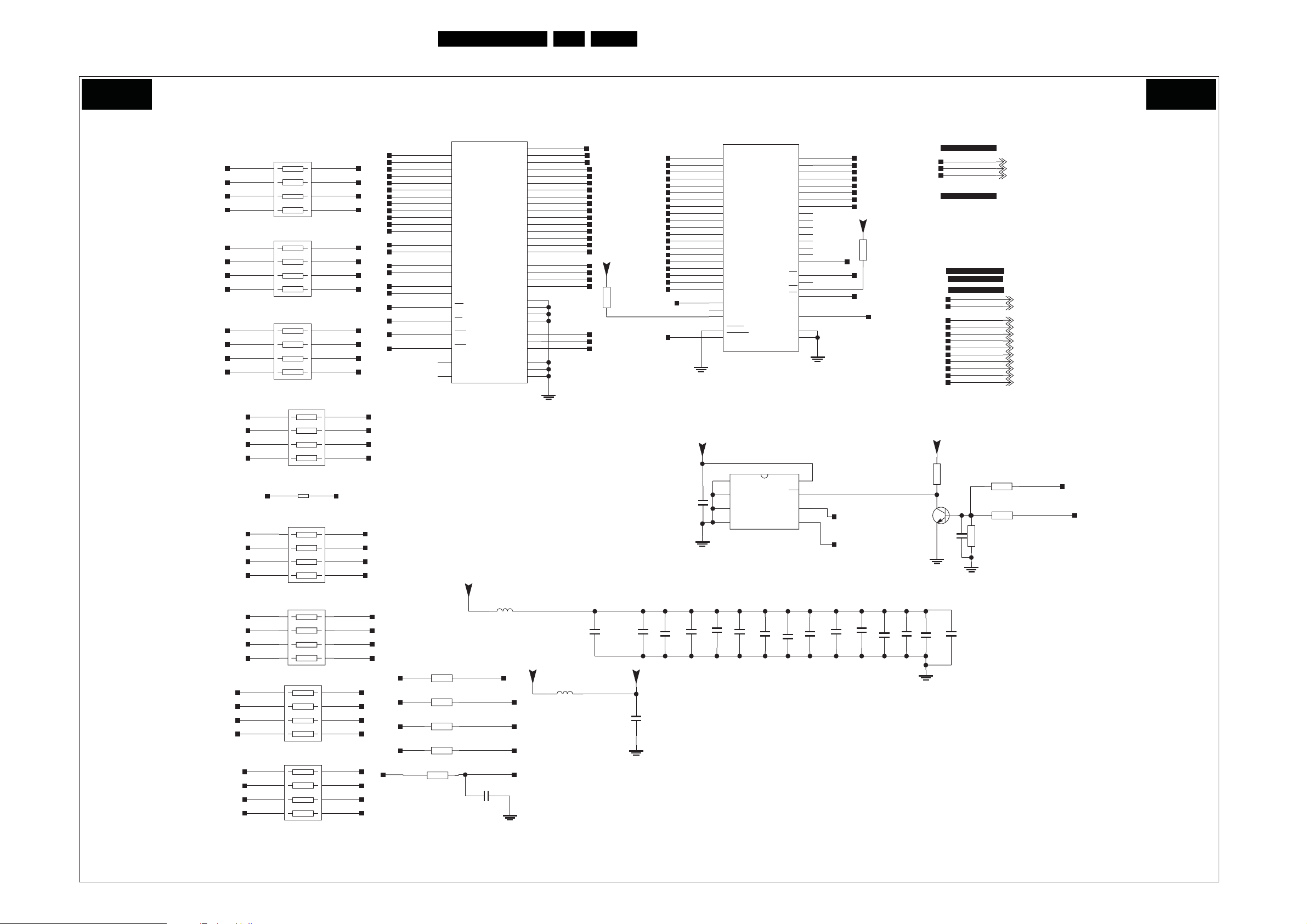
Circuit Diagrams and PWB Layouts
SSB: DDR Memory & Flash
29TCM1.0E LA 7.
B03 B03
DDR MEMORY & FLASH
NOTE:R33 is mounted only for 29lv160 Flash
A_RA0
A_RA1
A_RA2
A_RA3
A_RA7
A_RA6
A_RA5
A_RA4
A_RA11
A_RA9
A_RA8
A_DQ12
A_DQ13
A_DQ14
A_DQ15
A_WE#
3 6
2
1
3 6
1
3 6
1
A_DQ0
A_DQ1
A_DQ2
A_DQ3
A_RA10
A_DQ4
A_DQ5
A_DQ6
A_DQ7
A_DQ9
A_DQ10
A_DQ11
A_CAS#
A_RAS#
54
7
8
R42
22R
54
72
8
R213
22R
54
72
8
R214
22R
3 6
1
47R
R215
R28
22R
D_RA10
3 6
1
47R
R216
3 6
1
47R
R217
3 6
1
47R
R218
3 6
1
R44
22R
D_RA0
D_RA1
D_RA2
D_RA3
D_RA7
D_RA6
D_RA5
D_RA4
D_RA11
D_RA9
D_RA8
D_DQ0
54
D_DQ1
D_DQ2
72
D_DQ3
8
D_DQ4
54
D_DQ5
D_DQ6
72
D_DQ7
8
54
72
8
D_DQ12
54
D_DQ13
D_DQ14
72
D_DQ15
8
D_WE#
54
D_CAS#
D_RAS#
72
D_CS#A_CS#
8
D_DQ8A_DQ8
D_DQ9
D_DQ10
D_DQ11
D_RA0
D_RA1
D_RA2
D_RA3
D_RA4
D_RA5
D_RA6
D_RA7
D_RA8
D_RA9
D_RA10
D_RA11
D_BA0
D_BA1
D_DQM0
D_DQM0
D_CKE
D_CLK
D_WE#
D_CS#
D_CAS#
D_RAS#
23
24
25
26
29
30
31
32
33
34
22
35
20
21
39
15
37
38
16
19
17
18
36
40
R29
A_BA1 D_BA1
A_BA0
A_DQM0
R25
R26
A_CKE
A_CLK
75R
R27
U7
A0
A1
A2
A3
A4
A5
A6
A7
A8
A9
A10/AP
A11
BA0
BA1
UDQM
LDQM
CKE
CLK
WE
CS
CAS
RAS
NC1
NC/RFU
K4S641632K
DV33B
22R
22R
22R
22R
CB74
L10A
1000UR
D_BA0
D_DQM0
D_CKE
D_CLK
12P
2
4
5
7
8
10
11
13
42
44
45
47
48
50
51
53
3
9
43
49
6
12
46
52
1
14
27
28
41
54
SDV33_DDR
D_DQ0
D_DQ1
D_DQ2
D_DQ3
D_DQ4
D_DQ5
D_DQ6
D_DQ7
D_DQ8
D_DQ9
D_DQ10
D_DQ11
D_DQ12
D_DQ13
D_DQ14
D_DQ15
SDV33_DDR
SDV33_DDR
SDV33_DDR
SDV33_DDR
SDV33_DDR
SDV33_DDR
SDV33_DDR
FLASH_VCC
R33
10K
0.1U
CB76
DQ0
DQ1
DQ2
DQ3
DQ4
DQ5
DQ6
DQ7
DQ8
DQ9
DQ10
DQ11
DQ12
DQ13
DQ14
DQ15
VDDQ1
VDDQ2
VDDQ3
VDDQ4
VSSQ1
VSSQ2
VSSQ3
VSSQ4
VDD1
VDD2
VDD3
VSS1
VSS2
VSS3
SB33B FLASH_VCC
L27
120RR24
CB87
0.1U
CB77
0.1U
FLASH_VCC
0.01U
CB84
F_A1
F_A2
F_A3
F_A4
F_A5
F_A6
F_A7
F_A8
F_A9
F_A10
F_A11
F_A12
F_A13
F_A14
F_A15
F_A16
F_A17
F_A18
F_A19
F_A20
F_A21B
CB78
0.1U
SB33B
0.1U
CB75
CB85
25
24
23
22
21
20
19
18
48
17
16
10
13
14
47
12
0.01U
8
7
6
5
4
3
2
1
9
U8
A0
A1
A2
A3
A4
A5
A6
A7
A8
A9
A10
A11
A12
A13
A14
A15
A16
A17
A18
A19
NC
NC1
NC2
BYTE
RESET
S29AL016M
U10
1
E0/NC
2
E1/NC
3
E2/NC
4
VSS
M24C32MN
SYSTEM EEPROM
0.1U
CB86
0.01U
CB79
D15/A-1
RY/BY#
VCC
GND
GND1
VCC
SCL
SDA
0.01U
CB80
D10
D11
D12
D13
D14
D0
D1
D2
D3
D4
D5
D6
D7
D8
D9
OE
WE
CE
WC
CB88
29
31
33
35
38
40
42
44
30
32
34
36
39
41
43
45
28
15
11
26
37
27
46
8
7
6
5
0.01U
F_D0
F_D1
F_D2
F_D3
F_D4
F_D5
F_D6
F_D7
F_A0
F_OE#
IOWR#
IOCE#
FLASH_VCC
SCL
SDA
0.1U
CB81
FLASH_VCC
R35
10K
SYSROMWP
0.01U
CB118
F_D[0:7]
A_RA[0:11]
A_BA[0:1]
A_DQ[0:15]
IOCE#
F_OE#
IOWR#
F_A[0:21]
A_DQM0
A_CLK
A_CKE
A_CS#
A_RAS#
A_CAS#
A_WE#
FDAT
RXD
TXD
SCL
SDA
IOCE#
F_OE#
IOWR#
A_DQM0
A_CLK
A_CKE
A_CS#
A_RAS#
A_CAS#
A_WE#
FDAT
RXD
TXD
SCL
SDA
SB33B
10K
10K
10K
R83
R38
EEPROM_ENM
H : WP DISABLE
L : WP ENABLE
EEPROM_EN
R36
22K
C
BT3904
Q5
B
E
R41
0.1U
C78
0.1U
CB82
0.01U
CB119
0.1U
0.01U
CB83
CB120
I_17930_013.eps
220408
Page 30
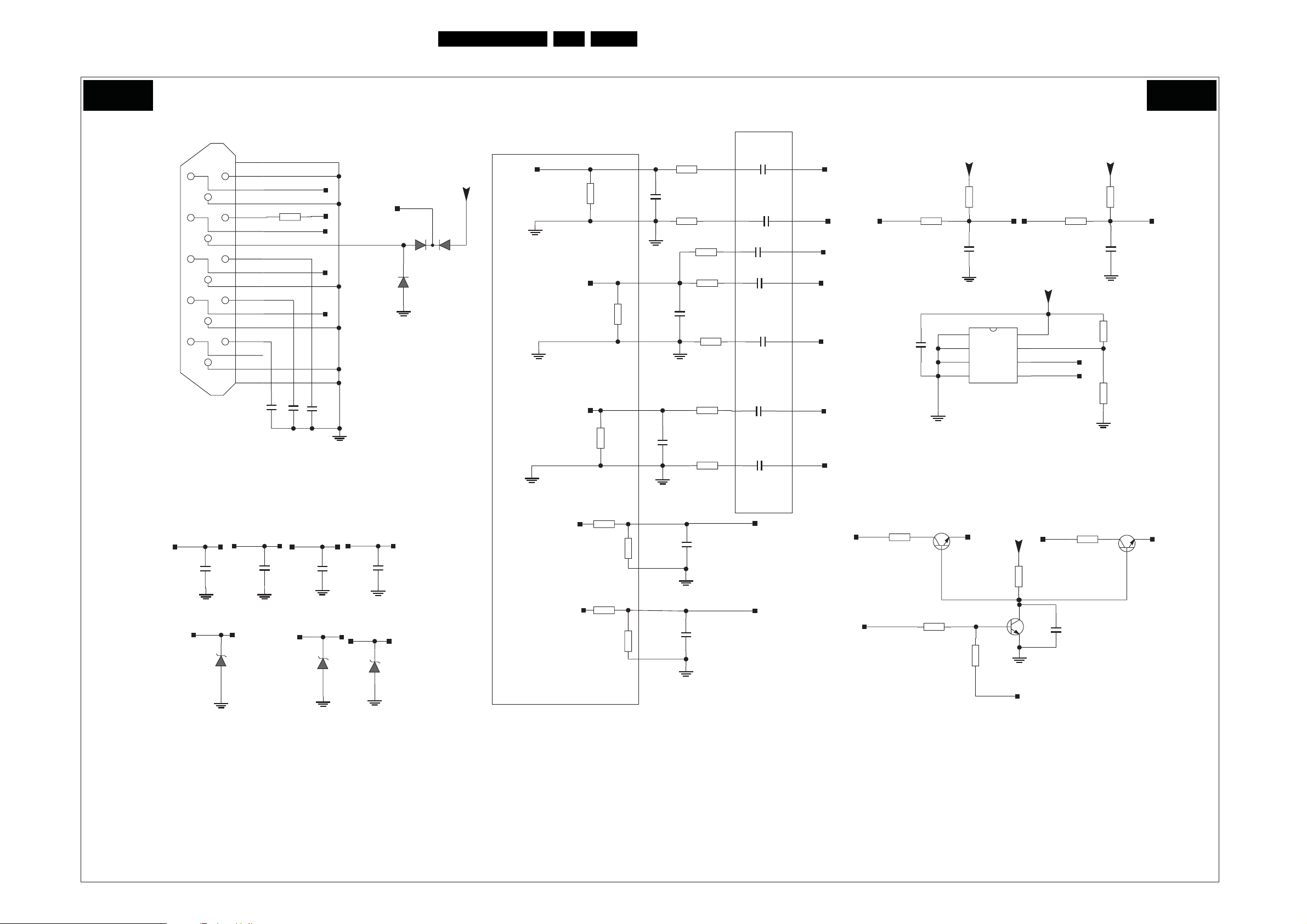
SSB: VGA Input
Circuit Diagrams and PWB Layouts
30TCM1.0E LA 7.
B04 B04
VGA INPUT
VGA IN
3
P3
RED
E
16
15
10
14
13
12
11
17
5
4
9
3
8
2
7
1
6
VGASCL_IN
GREEN
R9
1K
VSYNC
HSYNC
VGASDA_IN
BLUE
CS1
15P
VGAROMWP
CS2
15P
15P
C43
0.01U
RP
VGA_PLUGPWRVGA_PLUGPWR
RED
68R
R76
VCC
VGA_PLUGPWR
3
12
D16
BAV70
D17
D5V0S1
R77
82R
GREEN
R82
82R
CS3
BLUE
C44
5P
R73
100R
R81
0R
R79
68R
5P
C47
R74
100R
C59
0.01U
C46 4700P
C45
0.01U
C61
0.01U
RN
VGASOG
GP
GN
R93
100R
B
0.1U
CB115
R92
10K
VGASCL
47P
C52
VGA_PLUGPWR
U15
1
A0
2
A1
3
A2
4
GND
VGA_PLUGPWR
8
VCC
7
WP
6
SCL
5
SDA
VGASDA_INVG ASCL_IN
100R
VGARO MWP
VGASCL
VGASDA
R97
R96
10K
47P
C54
NC
R86
VGASDA
H : WP ENABLE
L : WP DISABLE
AT24C02
68R
R84
C48
0.01U
R89
BP
47K
2
4
R85
82R
C49
5P
R110
100R
C63
0.01U
BN
Near the MT8200
R87
510R
HSYNC
ESD-0402
VGASDA_IN
C257
GREEN
D202
HSYNC
C255
ESD-0402
C256
RED
5V6
D201
1
ESD-0402
5V6
VGASCL_INVSYNC
C258
ESD-0402
VSYNC
R90
510R
R88
2K
C50
BLUE
R91
2K
5V6
D203
Near the P3
C8
5P
VGAVSYNC#
47P
VGAHSYNC#
VGASCL_IN
DQ17
R605
100R
R006
100R
Q16
TXD
C143ZT
E
C
B
100R
R011
B
5VSB
R611
10K
C
Q15
E
VGASDA_IN
C143ZT
R608
200P
100R
C120
Q17
C143ZT
RXD
E
C
B
SLE
I_17930_014.eps
220408
Page 31
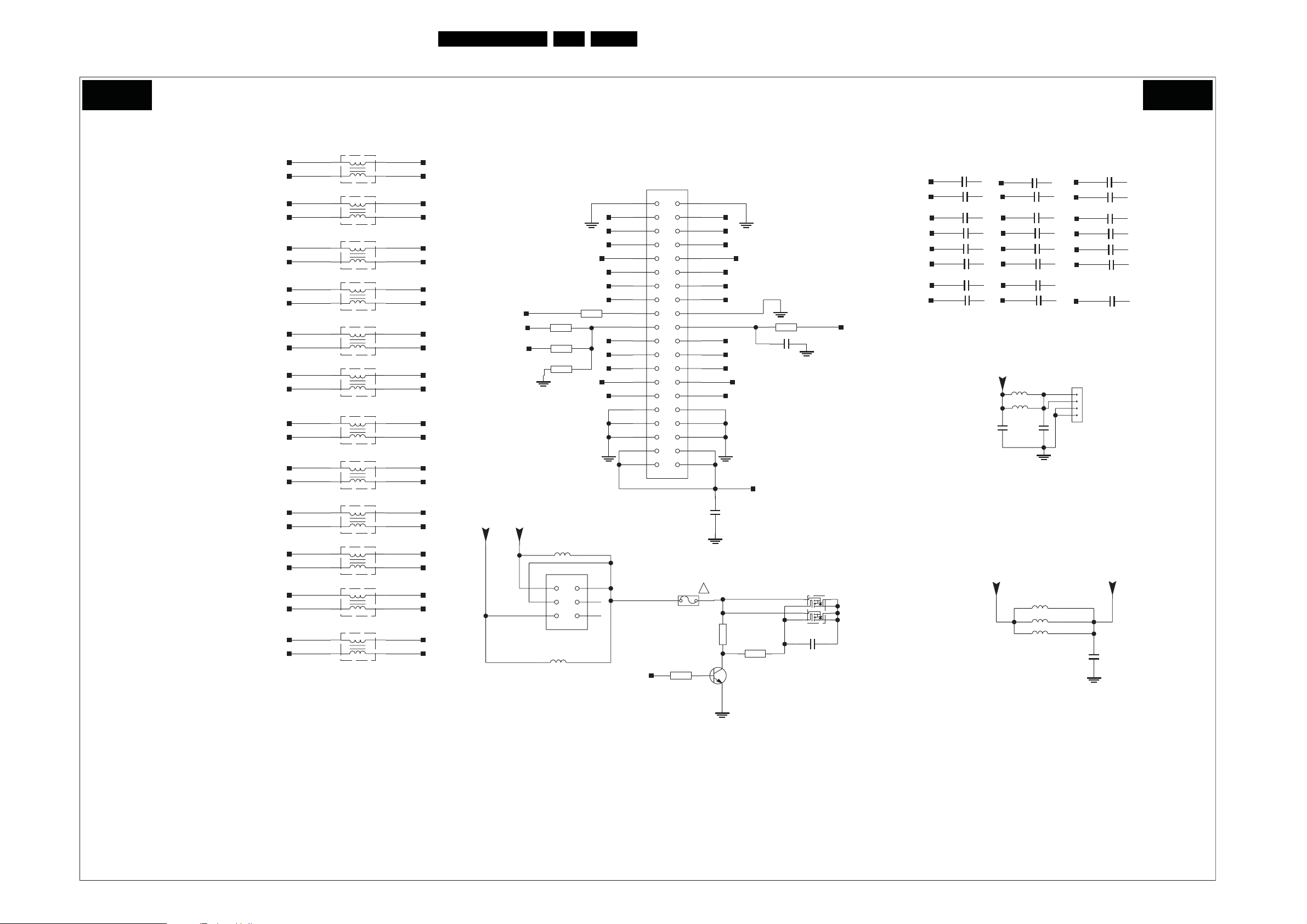
Circuit Diagrams and PWB Layouts
SSB: LVDS /TTL Interface
31TCM1.0E LA 7.
B05 B05
INTERFACE FOR LVDS\TTL
L201
ERO0
ERO1
ERO2
ERO3
AN0
AP0
AN1
AP1
AN3
AP3
AN4
AP4
AN2
A
AP2
CLK1-
CLK1+
CLK2-
CLK2+
AN7
AP7
AN5
AP5
AN6
AP6
Place these Termination Resistors as close to chip pin as possible
EXC24C
14
2
L202
EXC24C
14
2
L203
EXC24C
14
2
L204
EXC24C
14
2
L205
EXC24C
14
2
L206
EXC24C
14
2
L207
EXC24C
14
2
L208
EXC24C
14
2
L209
EXC24C
14
2
L210
EXC24C
14
2
L211
EXC24C
14
2
L212
EXC24C
14
2
3
3
3
3
3
3
3
3
3
3
3
3
ERO00
ERO11
ERO22
ERO33
AN00
AP00
AN11
AP11
AN33
AP33
AN44
AP44
AN22
AP22
CLK11-
CLK11+
CLK22-
CLK22+
AN77
AP77
AN55
AP55
AN66
AP66
12V
12V
GPIO_PANEL
R250
R245
R246
L608
NC/30R
NC
NC
NC
VCC
V33
DE
VCC
12
3
5
P504
L609
NC/30R
LV DS INTERFACE
P7
39
AP00
37
AP11
35
AP22
33
31
29 30
27
25
23
21
10K
R11
DE00
19
17
15
CLK22+ CLK22-
13
11
9
7
5
3
12
4
6
10K
GPIO9
F1
5.0A
R235
AP00
10P
40
AN00
38
AN11
36
AN22
34
CLK11-CLK11+
32
AN33AP33
ERO11ERO00
28
ERO33ERO22
26
24
22
AN44AP44
20
AN55AP55
18
AN66AP66
16
VCLK00
22R
R001
C80
10P/NC
VCLK
AN00
AP11
AN11
AP22
AN22
CLK11+
CLK11-
10P
10P
10P
10P
10P
10P
10P
14
AN77AP77
12
10
8
CT1
CT2
CT3
CT4
CT5
CT6
CT7
CT8
AP33
AN33
ERO00
ERO11
AP44
AN44
AP55
AN55
VCC
L610
L611
0.1U
10P
CT9
10P
CT10
10P
CT11
10P
CT12
10P
CT13
10P
CT14
10P
CT15
10P
CT16
30R
30R
C85
0.1U
C84
AP66
AN66
CLK22+
CLK22-
AP77
AN77
DE
1
2
3
4
P500
10P
10P
10P
10P
10P
10P
10P
CT17
CT18
CT19
CT20
CT21
CT22
CT23
6
4
LV DSVDD
CB140
0.1U
0.1U
VCC
C536
5V0
!
R236
22K
47K
BT3904
C
R220
Q12
B
E
U20
1
S1
2
G1
356
S2
4
G2
IRF7314
0.1U
C164
LVD SVDD
8
D1A
7
D1B
D2A
D2B
L561
L562
L563
30R
30R
30R
2
I_17930_015.eps
220408
Page 32
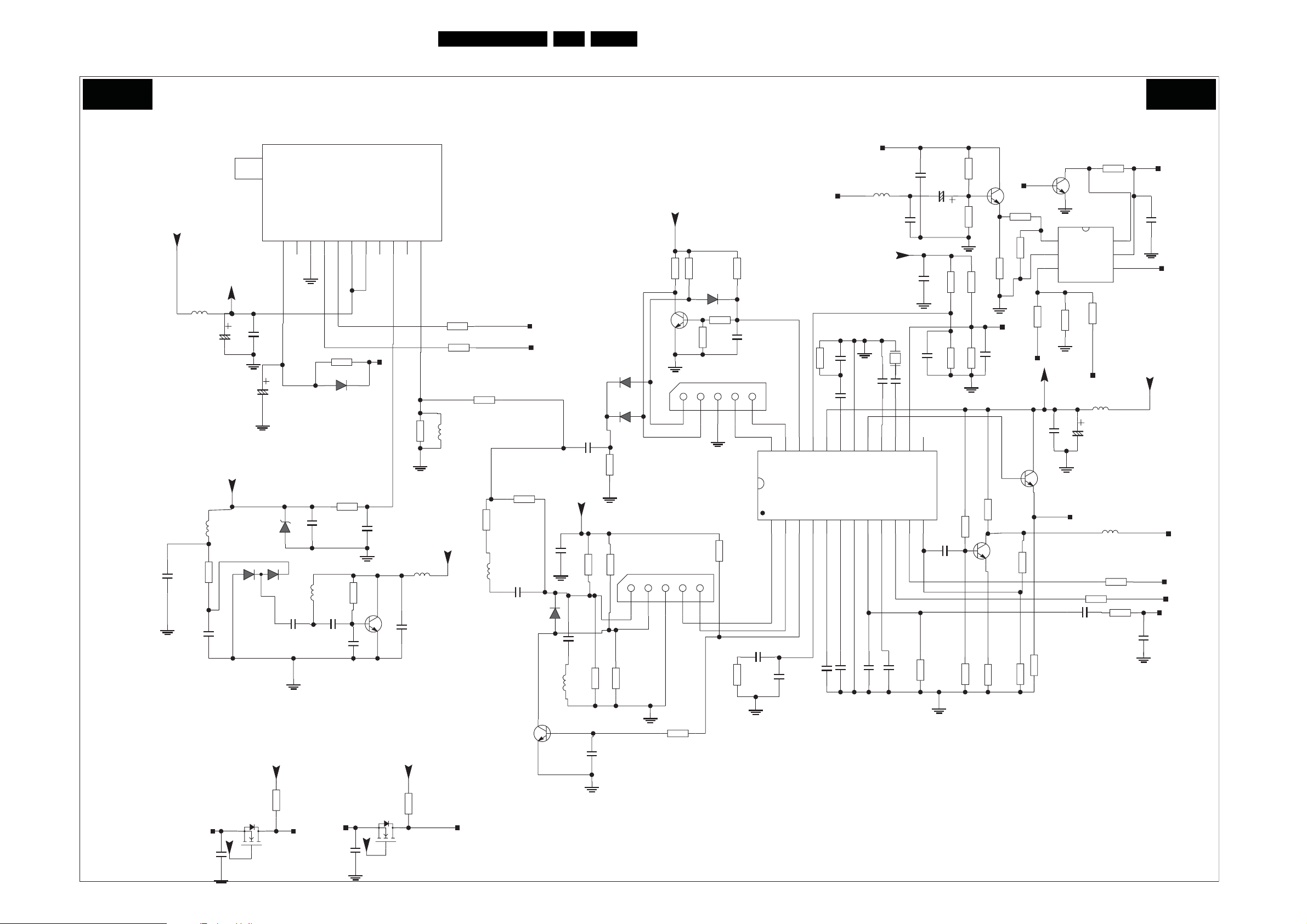
SSB: Tuner Block
Circuit Diagrams and PWB Layouts
32TCM1.0E LA 7.
B06 B06
TUNER BLOCK
D
C
0.1U/NC
C644
VCC
L601
1000UH
L605
R631
10R
47K
VCCOUT
16V
33V
C634
0.1U
C602
470U
1
4
16V
D613
0BAV99
3
5
0.1U
Z603
C603
C601
47U
D614
55C33V
2
C633
AGC
132
0.1U
NC1
C636
AS
1000P
102K
L604
4
C631
200P
SCL
12K
SDA
5
R601
D601
LL4148
R604
22K
R630
C632
MB1
6
100K
6800P
B
MB2
7
IF-AGC
0.1U
BC846B
C
E
8
C604
NC2
Q612
3
CVBS00
5VOUT
IF1
NC3
TU2
9
11
10
R80
6K8
Q611
C
B
E
R151
IN
R155
51R/NC
L14
1UH
R16
100R
100R
R17
0R
R632
SCL_TUNER
R10
33R
SDA_TUNER
R650
NC
C623
0.01U
5VOUT
R114
BA982
BA982
22K
BC847C
D611
D610
VCCOUT
L603
1000UH
4700P
C630
0UH
L606
C7
1000P
C628
BA592
D602
1000P
C625
0.56UH
L607
R634
2K2/NC
0.01U/NC
R635
2K2/NC
R633
2K2
X610
IN
IN/GND
GND
OUT1
54321
R636
0R/NC
6K8
680K
X611
R94
D612
BA982
R101
220K
IN/GND
R637
OUT2
R95
C609
GND
5K6/NC
R617
22K
0.01U
5K6
OUT1
54321
C617
0.01U
OUT2
U601
C614
C610
20
5
0.01U
0.22U
19
VP
DEEM
6
C620
1000P
VPLL
AFD
0.47U
330R
R117
24
22
21
23
AFC
OP2
SIF1
SIF2
VIF1
1
390P
C618
FMPLL
VIF2
OP1
4
2
3
C621
18
AGND
DGND
7
C619
L602
C612
17
AUD CVBS
8
1000P
12UH
0.47U
16
9
5VOUT
C606
5VOUT
X601
15
VAG C
TOP
10
0.1U
C607
68P
C611
4M
C613
20P
14
REF
TAG C
SDA
SCL
11
R645
C643
1000P/NC
0.01U
C622
13
12
2K2
16V
47U
0.1U
NC
SIOMAD
C627
1000P
C608
R620
TDA9886T
22K
22K
R621
R603
R606
R615
R616
R122
6K8
R120
1K5
22K
12K
100K
B
12K
B
IF-AGC
R156
180R
C
E
R119
51R
C
E
R607
330R
C640
0.01U
Q614
BC846B
Q601
BC847C
R609
220R
R612
330R
B
R646
NC
R123
2K2
OP1
R610
75R
CVBS00
5VOUT
BC847C
C
E
R614
220R
C
B
E
U602
1
B2
2
GND
R613
100R
0.01U
C642
Q610
CVBS00
MONO MONO
Q602
C124ET
74LVC1G3157
1K
R625
TU_CVBS_OUT
L49
200R
C605
220U
16V
R619
C615
1U
VCC
L51
R622
S
AB1
120R
R618
100R
4K7
6
5
43
R159
0R
5VOUT
0.1U
C616
TVCVBS0
VCCOUT
SCL_TUNER
SDA_TUNER
TV_AUDIO
0.01U
C599
SIF
B
SDA
C123
V33
QF4
2N7002
10P
VCC
R269
10K
SDA_TUNER
N-MOSFET
TUNER INTERFACE
SCL
C124
V33
2N7002
10P
QF3
VCC
N-MOSFET
R268
10K
SCL_TUNER
Q613
C124ET
C
B
E
OP1
R116
220R/NC
C624
1000P/NC
I_17930_016.eps
250408
Page 33
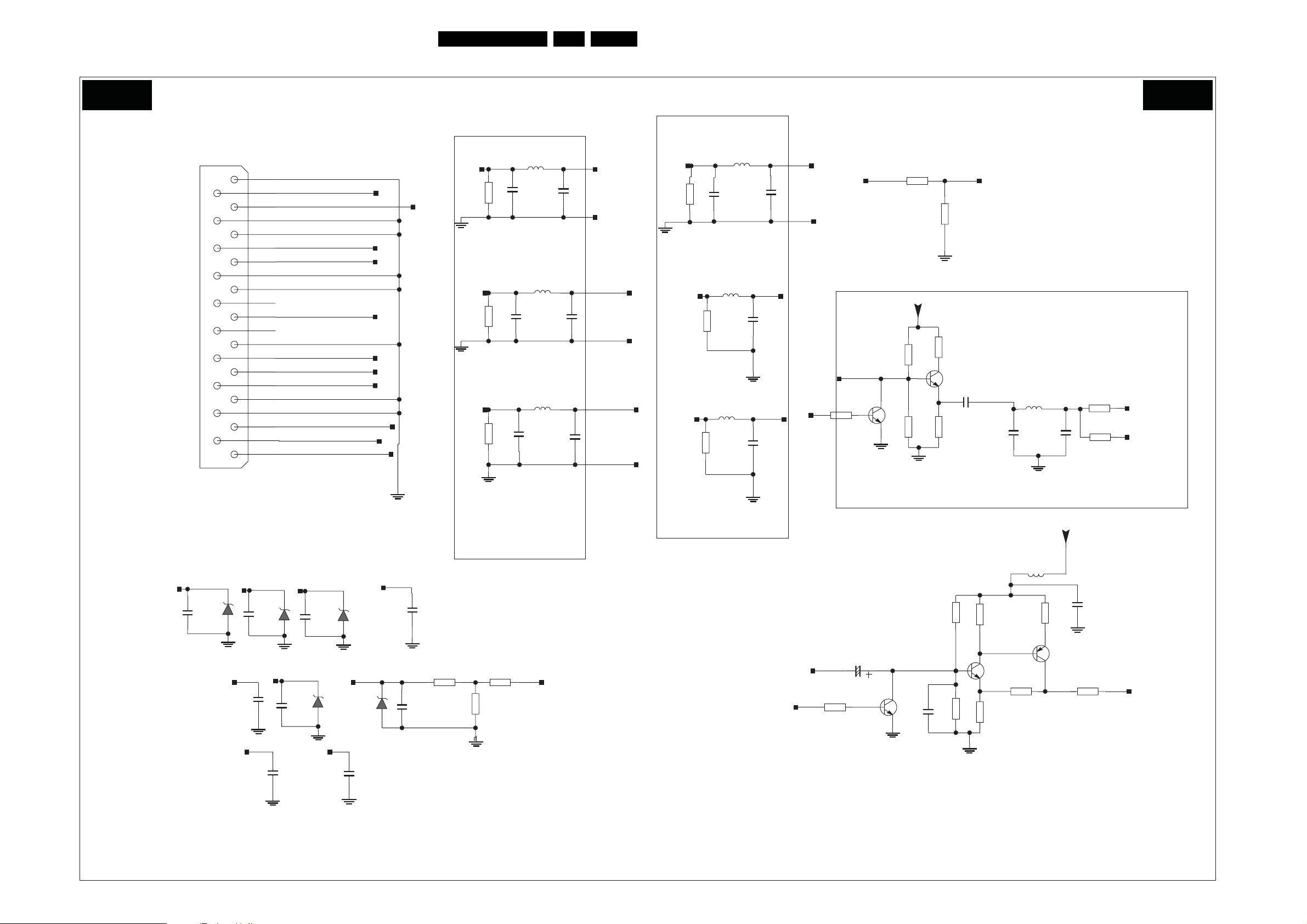
Circuit Diagrams and PWB Layouts
SSB: SCART Input Interface
33TCM1.0E LA 7.
B07 B07
SCART INPUT INTERFACE
1
12
2
13
3
14
4
15
5
16
6
17
7
18
8
19
9
20
10
21
11
SCART1
AV1_IN
CVBS_OUT_SCART1
SCART_FB1
SCT1_R_IN
SCT1_G_IN
SCT1_FS
SCT1_B_IN
AV1L_IN1
AVL_OUT_SCART1
AV1R_IN1
AVR_OUT_SCART1
SCT1_G_IN
R118
82R
SCT1_R_IN
R109
82R
SCT1_B_IN
R164
82R
15P
C169
C167
C168
15P
15P
L115
600R
600R
L113
L114
600R
L116
Y1_IN
15P
C93
GND
PR1_IN
15P
C94
C95
15P
GND
PB1_IN
GND
AV1 _IN
R106
82R
C58
AV1L_IN1 AV1L_IN
R165
AV1R_IN1
R43
47K
600R
15P
AV1_IN_GND To 8200 P181
L52
120R
47K
FB17
120R
C16 C18
47P
47P
15P
C90
AV1R_IN
AVC VBS1
GND
Near TNNER
DQ28
TV_AUDIO
R280
1K
SCT1_FS
C
B
E
Q9
BC846B
R247
R251
6K8
6K8
R160
33K
VCC
B
R113
R249
C
R252
ADCIN0
12K
TV_AUDIO_OUT
180R
Q18
C205
E
1U
BC846B
220R
2200P
C155
L107
2.2UH
2200P
C156
R203
1K
AVR_OUT_SCART1
R204
1K
AVL_OUT_SCART1
SCT1_R_IN
CS4
15P
5V6
D703
CVBS_OUT_SCART1
SCT1_G_IN
CS5
15P
5V6
D702
C79
ESD
AVR_OUT_SCART1
C118
SCT1_B_IN
15P
AV1_IN
CS7
15P
5V6
D704
AVL_OUT_SCART1
4700P/NC
B
L46
1.8UH
0
R200
VCC
C176
E
BT3906
Q14
C
CVBS_OUT_SCART1
0.1U
75R
R150
Near the SCART1
SCT1_FS
CS6
5V6
D701
C119
SCART_FB1
4700P/NC
5V6
D705
C12
ESD
R126
CS8
15P
The GND connect to U6.151 PIN
R127
75R
R398
100R0R
SCART_FB
Near the SCART1
TU_CVBS_OUT
1K
DQ28
TV_CVBS_OUT
R197
6V3
47U
C66
R281
C
Q8
B
E
BC846B
330P
C177
R196
20K
12K
B
1K
R198
R201
1K
C
Q2
BT3904
E
Near The SCART PIN
R146
1.2K
I_17930_017.eps
220408
Page 34
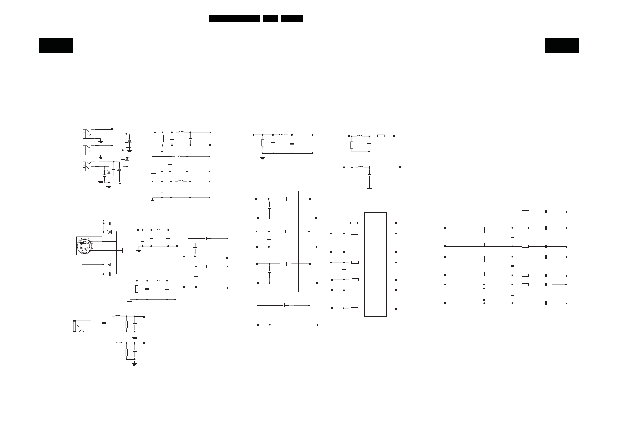
Circuit Diagrams and PWB Layouts
SSB: AV & S-Video & PC Audio Input
34TCM1.0E LA 7.
B08 B08
AV & S_VIDEO & PC-AUDIO INPUT
5
AV3 INTERFACE
P303
RED
RED
WHITE
BLUE
B
YELLOW
GREEN
S VIDEO INTERFACE
P6P6
EARPHON INTERFACE
P003
AV3R_IN1
9
8
3
7
6
2
5
4
1
6
2
5
7
1
3
4
1
VGAR_IN
2
VGAL_IN
3
PG0
D304
SYIN
AV3L_IN1
AV3_IN1
CS11
15P
5V6
D302
15P
5V6
CS13
5V6
D303
15P
CS14
PR0
CS9
15P
5V6
D307
PB0
CS10
15P
5V6
D306
CS12
15P
5V6
D305
R112
82R
L63
120R
R199
1000P
C71
47K
L62
120R
VGALL
SYIN
VGARR
R107
82R
AV3_IN1
PG0
PR0
L39
15P
C126
YO_GND To 8200 P171
L42
15P
C128
C0_GND To 8200 P171
600R
600R
R379
R167
R168
82R
82R 82R
L304
120R
47P
C301
L55
2.2UH
15P
C130
C132
15P
C97
15P
C96
C131
L56
2.2UH
15P
Y0
C0
47P
C98
15P
15P
C133
GND
YO_GND
GND
C0_GND
Y0
C174
C0
C175
AVCV BS3
AV3_IN_GND To 8200 P181
Y0_IN
GND
YO_GND To 8200 P171
PR0_IN
GND
¸Äºó
Near the MT8201
ɾ³ý
C92
0.047U
NC
To 8200 P171
C102
0.047U
NC
To 8200 P171
¸Äºó
Y0_IN
GND
PB0_IN
GND
GND
PR0_IN
AV3R_IN1
15P
C64
15P
C75
15P
C88
AV3L_IN1
R389
47K
R399
0R
68R
100R
68R
100R
47K
R104
100R
68R
FB302
R108
R130
R115
R131
R124
R133
R388
120R
120R
INTERFACE FOR SCT1 RGB
1K
47P
C304
R166
1K
47P
C306
Near the MT8200
C56
4700P
C62
0.01U
C99
0.01U
C72
0.01U
C100
0.01U
C83
0.01U
C101
0.01U
AV3R_IN
AV3L_IN
SOY0
Y0P
Y0N
PB0P
PB0N
PR0P
PR0N
INTERFACE FOR USB
Y1_IN
GND
PB1_IN
GND
PR1_IN
GND
15P
C108
15P
C107
15P
C116
SCART RGB INPUT
0R
68R
100R
68R
100R
68R
100R
R129
R1
R135
R138
R148
R143
R139
C91
4700P
C104
0.01U
C74
0.01U
C60
0.01U
C110
0.01U
C113
0.01U
C111
0.01U
Near the MT8201
SOY1
Y1P
Y1N
PB1P
PB1N
PR1P
PR1N
L57
C170
C171
C173
C134
47P
330P
330P
15P
Near the MT8200
2.2UH
C73
0.047U
15P
C135
AV3_IN_GND To 8200 P181
C57
0.047U
To 8200 P181
CVBS1
To 8200 P181
C81
0.047U
CVBS3
PB0_IN
GND
CVBS0
To 8200 P181
PB0
R169
82R
TVCVBS0
GND
AVCV BS1
SY0
GND
SC0
AVCVBS3
GND
CVBS INPUT
C106
C112
0.047U
330P
CVBS2
To 8200 P181
AVCVBS2
GND
TCLV1.0
R219
1000P
C70
47K
I_17930_018.eps
220408
Page 35
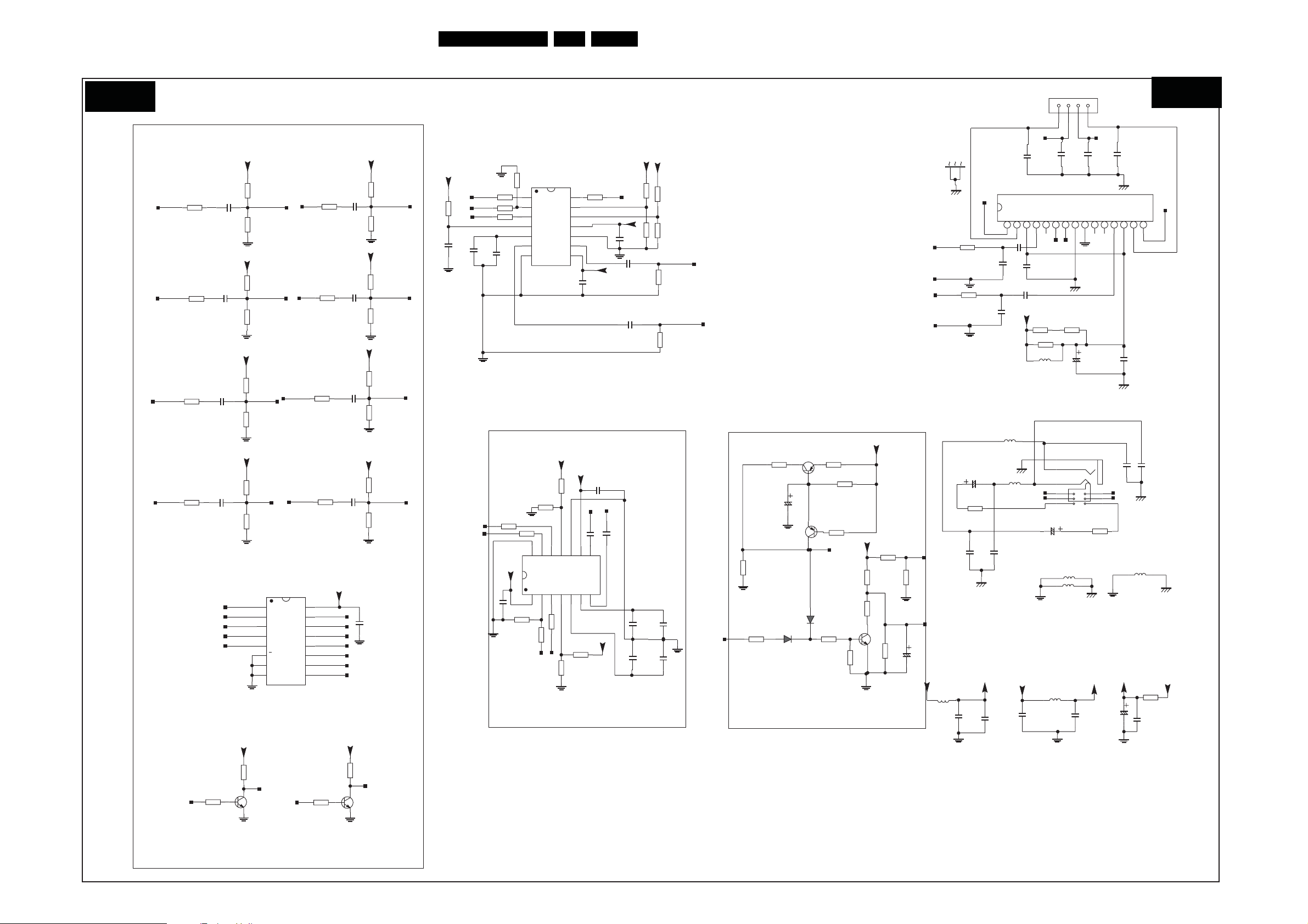
Circuit Diagrams and PWB Layouts
SSB: Audio / Power / Headphone
35TCM1.0E LA 7.
B09
AUDIO SWITCH & POWER AMPLIFIER & HEADPHONE INTERFACE
33R
R021
DACVL
R019
R030
10K
R017
U003
10K
1
2
3
4
5
6
7
33R
DAC
U002
LRCLK
DIN
BCLK
DEEMPH
ENABLE
VMID
ROUT
AGND
WM8501
R013
10K/NC
14
13
MCLK
DGND
DVDD
SDATO
1
234
R40
33R
DOUT
10K/NC
R016
MCLK
FORMAT
DVDD
DGND
LOUT
AVDD
DACVL
R014
10K
12
LRCLK
BCLK
R020
33R
AOBCLK
11
NOHP
FMT
14
13
12
11
10
9
8
ADCVA
ADCVA
10
9
AVDD
AGND
CAP
VREF
5
6
R015
10K
ADC
33R
C012
0.1U
C009
A_IN_L
R031
8
7
0.1U
LIN
RIN
C003
1U
DACVL
AOMCLK
DACVL
ADCVA
A_IN_R
1U
WM8738
C919
C920
C004
0.1U
1U
C013
1U
DACVL
0.1U
R032
R033
C007
C008
0.1U
V33
10K/NC
10K
R034
R035
R008
R009
V33
10K/NC
10K
NC/33K
NC/33K
DAOUTL
C930
1U
C931
1U
DAOUTR
AV1R_IN
AV1L_IN
AV3R_IN
AV3L_IN
C924
C926
C928
SWV120
AV1L
AV3L
GPIO1_SW
GPIO2_SW
SWV120
C922
SWV120
V33
R029
AOLRCK
R5
22K
2U2
2U2
2U2
2U2
C65
0.1U
R6
15K
SWV120
R8
22K
R7
15K
SWV120
R191
22K
R190
15K
SWV120
R189
22K
R4
15K
AVS_L_IN
AVS_R_IN
VGA_R
VGA_L
R026
47K
C010
0.1U
1
A0SDATA 3
AOBCLK
1U
AOLRCK
C929
AOMCLK
C001
33R
R028
33R
R027
33R
C011
0.1U
0.1U
SWV120
2
2
R182
C921
R170
4K7
R171
4K7
C925
R175
4K7
C927
R177
4K7
C923
22K
2U2
2U2
2U2
2U2
AV1R
R179
15K
SWV120
22K
R34
15K
R39
SWV120
R185
22K
R3
15K
SWV120
R183
22K
R184
15K
AVS_R_IN
A_IN_R
AV3R
VGA_R
SWV120
AV1R
AV1L
AV3R
AV3L
U16
1
Y0B
2
Y2B
3
ZB
4
Y3B
5
Y1B
6
E
7
VEE
8 9
VSS A1
HEF4052B
VGARR
VGALL
VDD
Y2A
Y1A
Y0A
Y3A
R172
6K8
AVS_L
R174
6K8
AVS_R
R176
4K7
R178
4K7
16
AVS_L_IN
15
14
VGA_L
A_IN_L
13
ZA
12
11
10
A0
MUTE
R005
1K
4K7
R018
OUT2-
14
6800
PGND
L2
200R
CE4
47R
0.1U
OUT2+
15
R48
CB4
B09
REAR
PGND
12V
P4
123
4
C207
4700P/NC
MUTE
STBY
SS
MS
PGND
R025
2R7
25V
1
2
3
9
8
7
CE10
16V
L70
200R
L71
200R
Near the P502
30R
RSP
C208
4700P/NC
PW_GND
1000U
P004
PGND
C005
1U
S_GND
CE596
100R
DACVL
NC2
6
5
4
R141
C209
4700P/NC
PGND
NC3
VCC2
IN2
11
10
13
12
VS12+
0.1U
C196
PGND
6800P
C024
C023
RSPLSP
REAR
Near the P502
SWV120
330U
16V
LSP
C206
1
2
Y001
PGND
R037
470R
DAOUTL
R039
470R
DAOUTR
12V
16V
BT3906
D2
LL4148
220U
Q001
Q003
C
CCE002
BT3906
E
B
E
B
C
HW_MUTE
LL4148
D3
10K
R010
R004
4K7
220
R007
10R
FB003
CE11
47U
16V
R142
100R
C026
C025
4700P/NC
PGND
ADCVA
ADCVA
1U
C932
0.1U
R003
4K7
12V
R025
BT3904
10K
12V
R022
10K
R036
0R
C
Q002
B
E
R12
10K
R024
10K
SS
R026
10K
MS
C006
16V
10U
VCC
R2
4K7
4700P/NC
U001 TDA7266
OUT1-
LEAR
C017
C015
4700P/NC
C002
1000P
1000P
L21
OUT1+
1
C018
600
L22
600
C109
C933
2
1U
PGND
V33
1U
VCC1
3456789
0.1U
1U
12V
12V
IN1
NC1
C195
R023
2R7
R20
1R
L68
200R
LEAR
47U
HEADPHONE INTERFACE
FB004
SCL0
R186
47K
R188
1K
GPIO1_SW
C
Q10
B
BT3904
E
SDA0
R37
47K
R187
1K
GPIO2_SW
C
Q1
B
BT3904
E
I_17930_019.eps
250408
Page 36
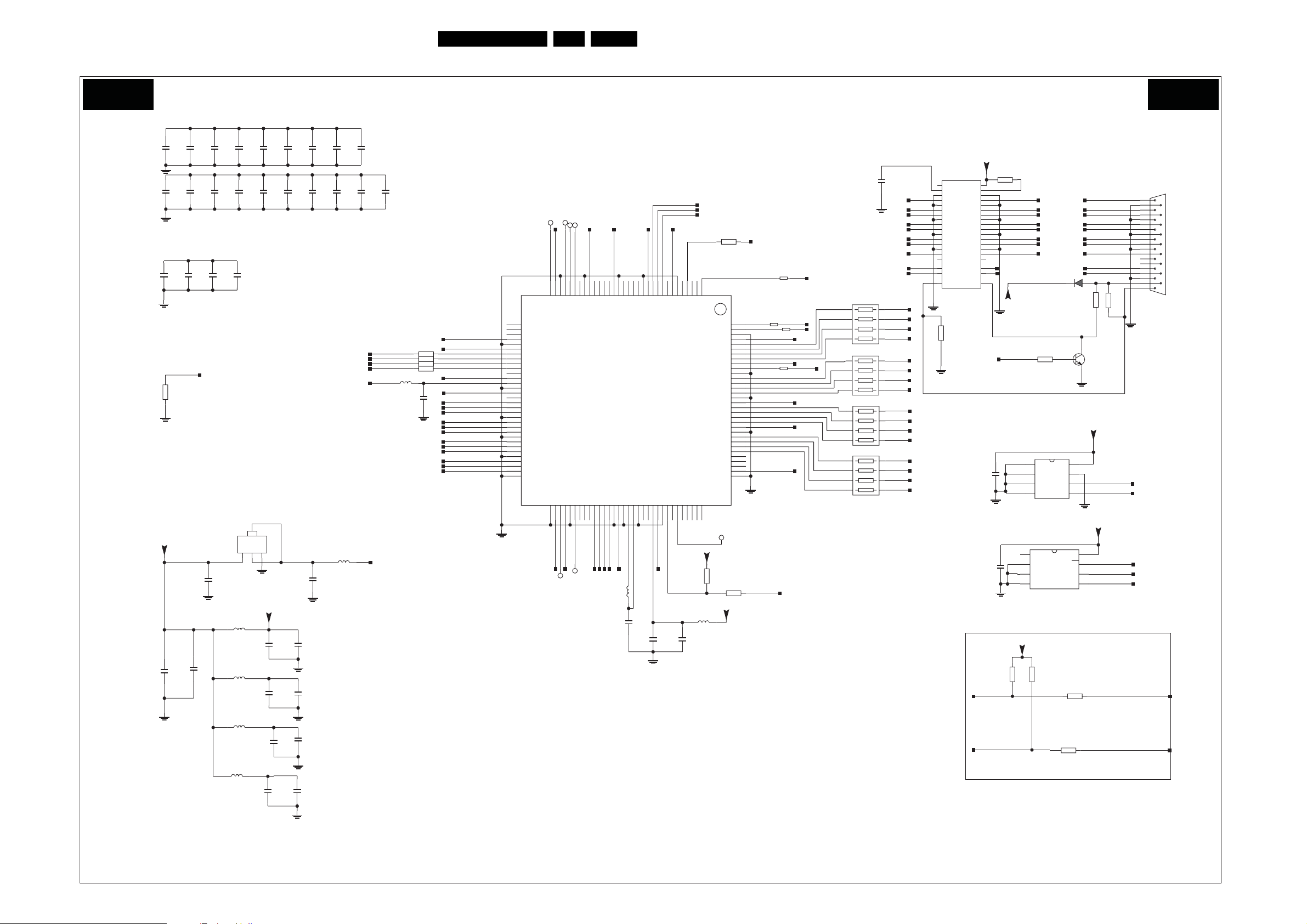
SSB: HDMI Input MT8293
Circuit Diagrams and PWB Layouts
36TCM1.0E LA 7.
B10 B10
HDMI INPUT MT8293
VCC18
0.1U
0.1U
C28
1000P
CB56
0.1U
CB92
CB93
CB94
0.1U
CB95
0.1U
IOVCC
C30
1000P
0.1U
0.1U
CB99
CB98
CB100
0.1U
CB101
0.1U
CB102
0.1U
AVCC
0.1U
CB89
0.1U
1000P
C26
CB90
C27
1000P
CI2CA
R55
4K7
CB96
CB103
0.1U
0.1U
0.1U
CB97
0.1U
CB104
1000P
C29
0.1U
CB105
SDA
SCL
9993_SDA
9993_SCL
VCC18
C31
1000P
L33
120R
0.1U
CB111
R58 0R
R59
R60 0R
R62
VCC18
CI2CA
0R
0R
PLUGPWR
PVCC
AVCC
CLOCKCLOCK+
AVCC
DATA0DATA0+
AVCC
DATA1DATA1+
AVCC
DATA2DATA2+
33
34
35
36
37
38
39
40
41
42
43
44
45
46
47
48
49
50
51
52
53
54
55
56
57
58
59
60
61
62
63
64
GPIO2
GPIO1
NC2
CVCC18_5
CGND18_5
CI2CA
CSDA
CSCL
DSDA
DSCL
NC4
PWR5V
CVCC18_2
PGND
PVCC
RSVD
AVCC2
RXCRXC+
AGND3
AVCC3
RX0RX0+
AGND2
AVCC1
RX1RX1+
AGND1
AVCC
RX2RX2+
AGND
PLUGPWR
U40
38
DDC_SDA
NC1
37
NC
36
GND9
35
D2+1
34
GND8
33
D2-1
32
D1+1
31
GND7
30
D1-1
29
D0+1
28
GND6
27
D0-1
26
CLK+1
25
GND5
24
CLK-1
23
CE_OUT
22
CLK_OUT
21
DAT_OUT
R64
47K
0.1U
C53
HDCP_SCL
HDCP_SDA
13
14
NC3
CGND18_3
AUDPGND
XTALOUT
84
VCC18
CVCC18_3
XTALIN
12
85
11
KSCL
XTALVCC
86
10
9
KWP
KSDA
REGVCC
RSVDL
88
87
KWP
OSC_IN
R57
0R
27MHZ
IOVCC
R98
33R
VSYNC_HDMI
3
4
8
NC1
RESET#
89
1
2
576
VCNTL1
CEN
SOG_IN
OSC_IN
NC
IOVCC33_3
IOGND33_6
R99
33R
HSYNC_HDMI
VCC18
IOVCC
33R
VCC18
IOVCC
IOVCC
33R
R63
R100
DE_HDMI
HDMIODCK
VCNTL2
128
VCNTL3
127
CGND18_1
126
CVCC18_7
125
Q0
124
Q1
123
Q2
122
Q3
121
IOVCC33_2
120
ODCK
119
IOGND33_2
118
Q4
117
Q5
116
Q6
115
Q7
114
CGND18_2
113
CVCC18_1
112
Q8
111
Q9
110
Q10
109
Q11
108
IOVCC33_1
107
IOGND33_5
106
Q12
105
Q13
104
Q14
103
Q15
102
Q16
101
Q17
100
Q18
99
IOVCC33_5
98
IOGND33_4
97
SCDT
Q23
Q22
Q21
Q20
Q19
INT
93
94
92
95
96
90
91
RN9
22R
1
2
3
45
RN10
22R
1
2
3
45
RN11
22R
1
2
3
45
RN12
22R
1
2
3
45
Z14
Z13
Z11
Z12
T
T
TT
8293_GPIO4
IOVCC
8293_GPIO3
IOVCC33_6
GPIO3
CGND18
CVCC18
65
VCC18
IOVCC
8293_GPIO5
8293_GPIO6
23262728293224
25
30
31
IOGND33
GPIO4
IOVCC33
MUTE
67
66
68
GPIO5
IOGND33_3
69
GPIO6
SPDIF
GPIO7
SD3
71
CGND18_4
SD2
GPIO8
CVCC18_4
SD1
SD0
737078
74
72
GPIO9
WS
75
GPIO11
GPIO10
IOVCC33_7
SCK
76
2021221918
IOVCC33_4
IOGND33_7
MT8293
IOGND33_1
MCLK
77
U12
79
17
GPIO13
GPIO12
CGND18_6
CVCC18_6
80
15
16
GPIO14
AUDPVCC18
818283
DATA2+
DATA2DATA1+
DATA1DATA0+
DATA0-
CLOCK+
CLOCK-
DDC_SCL
8
VI0
7
VI1
6
VI2
VI3
8
VI4
7
VI5
6
VI6
VI7
8
VI8
7
VI9
6
VI10
VI11
8
VI12
7
VI13
6
VI14
VI15
1
2
3
4
5
6
7
8
9
10
11
12
13
14
15
16
17
18
1920
9993_SCL
9993_SDA
0R
R181
DATA2+
DATA2DATA1+
DATA1-
DATA0+
DATA0-
CLOCK+
CLOCK-
HDMI_PLUGPWR
HDMI_PLUGPWR
D21
LL4148
5V_SUPLY
LV_SUPLY
GND
D2+
GND1
D2-
D1+
GND2
D1-
D0+
GND3
D0-
CLK+
GND4
CLK-
CE_IN
CLK_IN
DAT_IN
HPD_INHPD_OUT
CM2021
DATA2+
DATA2-
DATA1+
DATA1-
DATA0+
DATA0CLOCK+
CLOCK-
DDC_SCL
DDC_SDA
1K
R66
4
PLUGPWR
R61
P1
1
RX2+
2
GND1
3
RX2-
4
RX1+
5
GND2
6
RX1-
7
RX0+
8
GND3
9
RX0-
10
RXC+
11
GND4
12
RXC-
13
NC1
14
NC2
15
DDCCLK
16
DDCDA
17
GND5
18
VCC
19
HPD
1K
HDMICAB
DQ30
R67
1K
C
Q6
B
BT3904
E
HDMI_PLUGPWR
U13
1
A0
2
0.1U
C36
A1
3
A2
4
GND
AT2 4 C 02
VCC
SCL
SDA
8
7
WP
6
DDC_SCL
5
DDC_SDA
DV33B
1.25x(1+48.7/110)=1.8V
0.1U
10U
C55
CB107
U11
LD1117S18
CB53
0.1U
4
4
A
GND/ADJ
OUT
VIN
123
R48=48R7
AVCC
CB108
0.1U
CB110
0.1UCB109
0.1U
AVCC
CB106
0.1U
IOVCC
REGVCC
PVCC
1000P
C34
1000P
C35
L29
120R
L30
120R
L31
120R
L32
120R
C51
1000P
1000P
L28
120R
VCC18
10U
IOVCC
SPDIF
VCC18
T
Z28
HDMISD0
T
Z27
C32
C33
HDMILRCK
HDMIBCLK
IOVCC
VCC18
HDMIMCLK
120R
L34
0.1U
CB113
0.1U
CB114
REGVCC
HDMIRST#
0.01U
C42
L40
DV33B
R70
120R
Z25
T
0.1U
R72
4K7
0R
DE_SOG
CB112
1
E0/NC
2
E1/NC
3
E2/NC
4
VSS
A
U14
M24C08
DV33B
HDMI_PLUGPWR
R50
R49
47K
47K
DDC_SCL
DDC_SDA
DV33B
8
VCC
7
KWP
WC
6
HDCP_SCL
SCL
5
HDCP_SDA
SDA
R54
0R
R56
0R
9993_SCL
9993_SDA
1
I_17930_020.eps
220408
Page 37
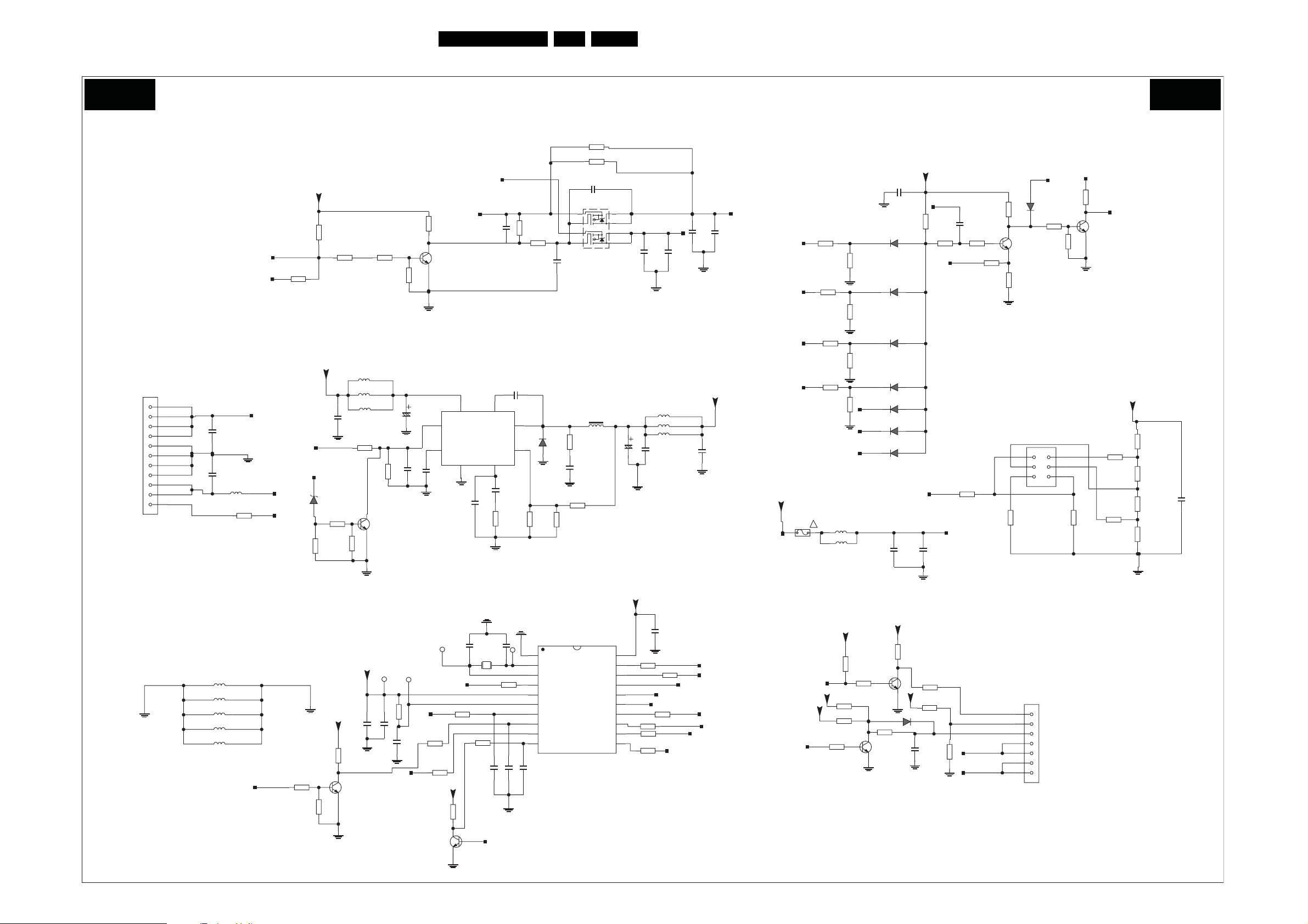
Circuit Diagrams and PWB Layouts
SSB: DC DC / MCU for Stby/Protect
37TCM1.0E LA 7.
B11 B11
DC DC/MCU FOR STANDBY/PROTECT
5VSB
NC
16V
GNDP
C200
R501
NC
R503
C
B
E
10K
C594
1000U
NC
C201
GNDP
P502
11
10
9
8
7
6
5
4
3
2
1
POWER CINCH
12V/4A
5V/2A
CONNECTOR
C161
0.1U
12V_IN
C160
0.1U
L54
30R
5V_PW
4K7/NC
R502
POWER_STBY
POWER_STBYC
5VSBIN
PRO
R551
10K
R19
4K7
R51
1K
12V
C512
0.1U
ON/OFF
VCC
3V9
D13
R307
10K
R306
R308
1K
PRO
L558
L559 30R
L560
R531
NC
B
10K
R552
4K7
30R
30R
R530
NC
C
Q22
BT3904
E
ON/OFF
Q505
BT3904
U501
7
8
R304
1R
R305
1R
5V_PW
0.1U
C520
R140
C538
NC
GNDP
R132
NC
U505
1
8
D1A
S1
G1
S2
G2
NC
R623
47K
2
3
4
IRF7314
L569
15UH
7
D1B
6
D2A
5
D2B
10U
C916
CE595
1000U
16V
GNDP
C502
L557
L556
L555
CB506
0.1U
0.1U
5V0
C992
30R
30R
30R
12V
10U
0.1U
C553
VCC
C537
0.1U
12V_IN
VCC
3K9
R289
R290
2K2
R291
2K7
DV33B
R292
4K7
R293
2K7
V33
R294
4K7
R295
2K7
SB33
R296
4K7
F2
5.0A
PANEL INVERTER POWER
L47
!
200R
L48
200R
VCC18
V18
SB18
LL4148
LL4148
LL4148
LL4148
LL4148
LL4148
LL4148
CB138
12V_IN
1U
R550
47K
C551
C204
IN
GND
C202
MP9583
100P
C203
R136
1
6
3.3NF
7K5
GNDP
BS
COMP
SW
2
EN
SS
4
GNDP
0.01U
FB
47K
R504
10U
C991
3
D1
S2L40U
5
GNDP
R134
15K
C178
D10
0.1U
D4
D5
D6
D7
D8
D9
0.1U
12V_IN
R297
100K
PANEL_SLT
12VPWR
0.1U
CB139
POWER_STBY
R298
C179
10K
0.1U
12V_IN
NC
RM22
R302
R299
10K
B
R300
8K2
R301
47K
C
BT3904
E
1K
Q20
RM23
750R
PRO
D11
LL4148
4K7
4
6
PM01
R194
R195
12
3
5
VCC
R193
10K
DEC
C
Q28
B
BT3904
E
10K
V33
RM30
1K
RM29
6K8
RM28
390R
RM24
100K
120R
RM25
RM27
390R
RM26
390R
0.1U
CM09
GNDP
L564
L565
L566
L567
L568
MADV33
5VSB
PWM1
V33
VCC
R231
4K7
PWM0
Inital pull up
5VSB
R238
R227
R226
10K
R239
4K7
NC
1K
B
0.1U
ZMX2
T
27P
CM01
5VSB
ZM5V
ZMRES
T
0.1U
RM02
CM10
10K
0.047U
T
LEDR
100R
C124ET
IR_INPUT
RM05
RM14
100R
30R
30R
30R
30R
30R
TO key BD
KEY2
RM21
10K
RM20
5VSB
10U
CM04
CM03
10K
RM19
C
QM01
B
BT3904
E
10K
Q19
5VSB
RM18
100R
10K
C
E
POWER_STBY
RM04
B
100R
SCO
SCT1_FS
XM01
RM06
8M
CM05
0.1U
C6
27P
100R
CM06
RM01
0.1U
ZMX1
T
CM07
0.1U
UM01
1
VSS
2
P121/X1
3
P122/X2
4
P123
5
VDD
6
#RESET/P34
7
P31/TI010/TO00/INTP2
9
P40
10
P41/INTP3
KA-9222
AVRE F
P20/ANI0
P21/ANI1
P22/ANI2
P23/ANI3
P130
P45
P44/RXD6P30/TI000/INTP0
P43/TXD6/INTP1
P42/TOH1
CM08
20
RM13
100R
19
18
PANEL_SLT
17
16
KEY2
15
SLE
RM08
100R
RM07
10K
EEPROM_ENM
100
RM16
100R
14
138
12
11
100R
RM09
RM12
COM
MUTE
SCL
SDA
DEC
VCC
R234
Back Light circuit
10K
C
R230
Q13
B
BT3904
100R
VCC
E
R232
LL4148
D20
CB137
1U
NC
DIMMING
R229
10K
C
Q11
BT3904
E
BL ON/OFF
SELECT
GND
R233
10K
12VPWR
1
2
3
4
5
6
7
P503
I_17930_021.eps
220408
Page 38
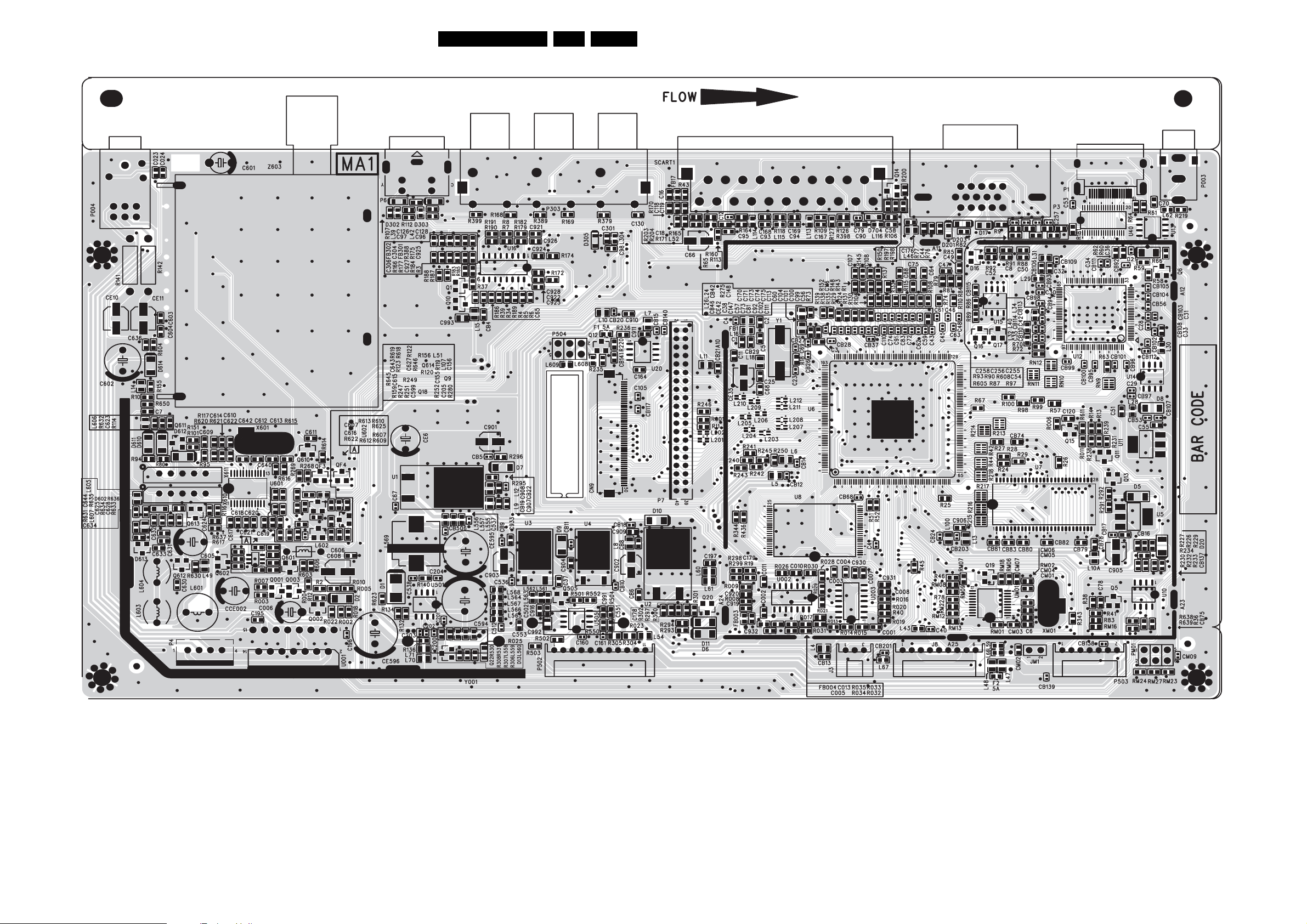
Circuit Diagrams and PWB Layouts
Layout Small Signal Board (Top Side)
38TCM1.0E LA 7.
I_17930_022.eps
220408
Page 39
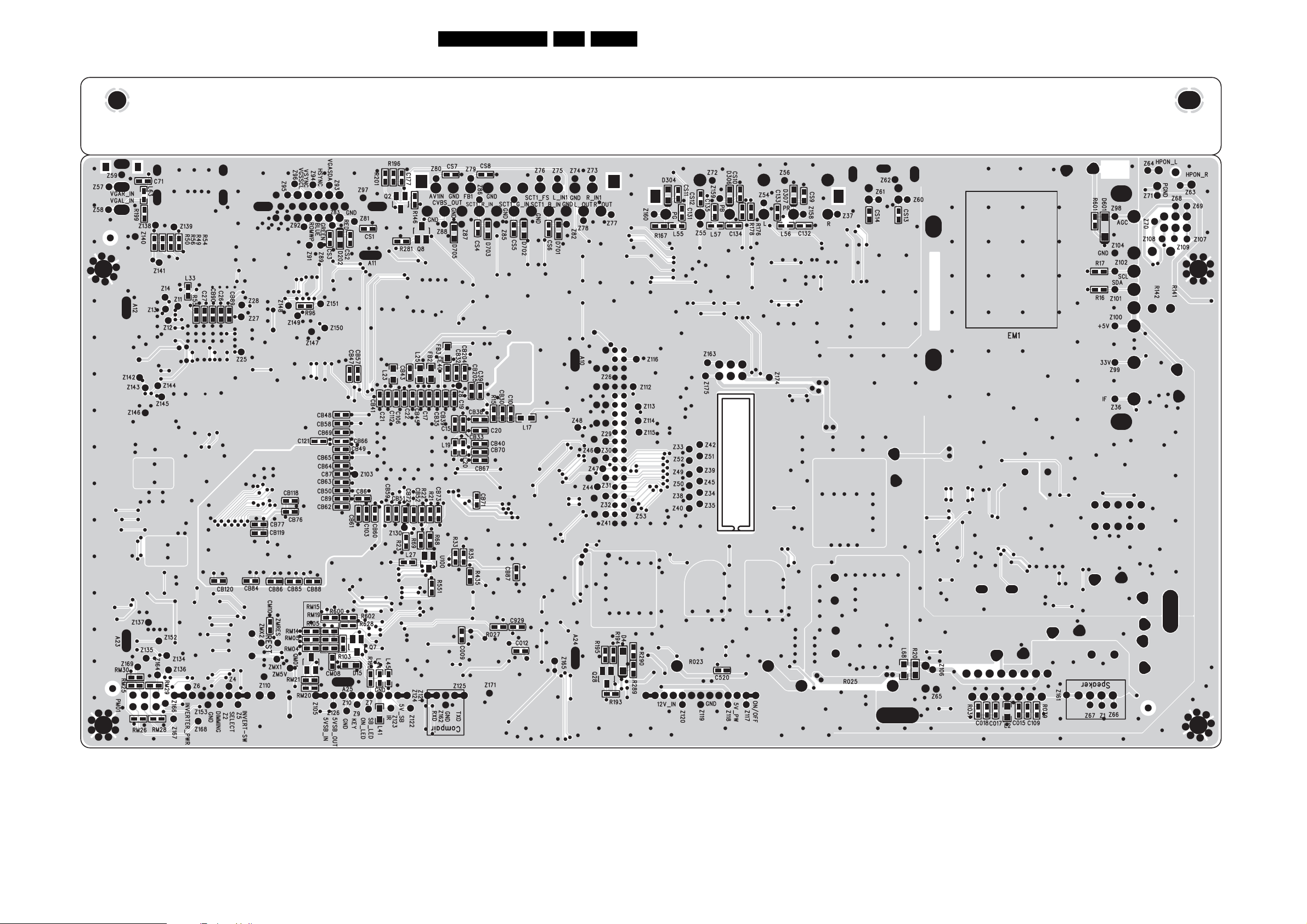
Circuit Diagrams and PWB Layouts
Layout Small Signal Board (Bottom Side)
39TCM1.0E LA 7.
I_17930_023.eps
220408
Page 40
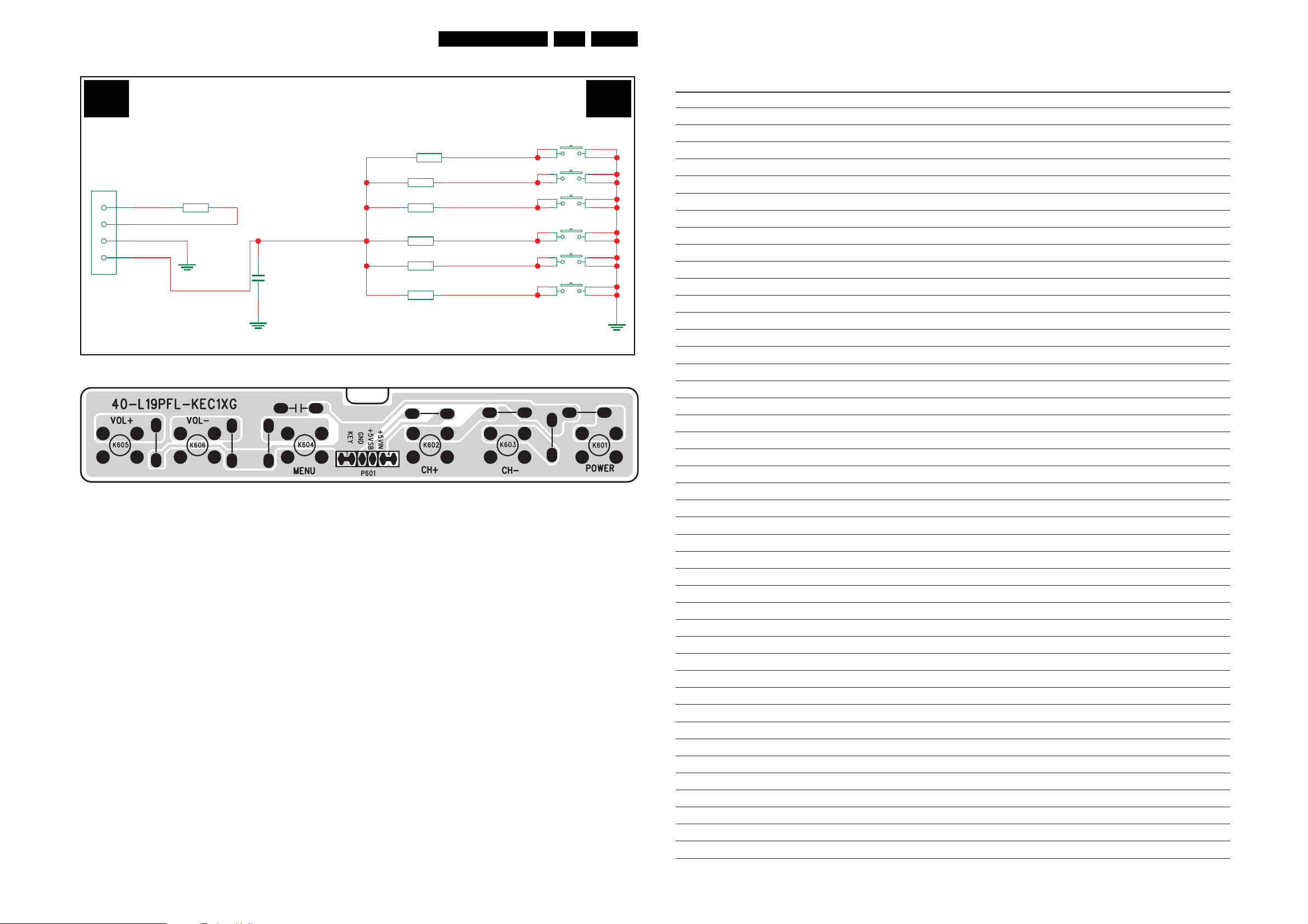
Circuit Diagrams and PWB Layouts
s
4
40TCM1.0E LA 7.
Keyboard Control Panel
KEYBOARD CONTROL
E E
Personal Notes:
P601
4
3
GND
2
1
5VIN
5VSB
KEY
0
R701
0.1U
C601
Layout Keyboard Control Panel (Top Side)
1K
1K5
2K7
4K3
7K5
R601
390R
R602
R603
R604
R605
R606
vol-
vol+
menu
ch-
ch+
POWER
K606
1
24
1
24
1
24
1
24
1
24
1
24
3
K605
3
K604
3
K603
3
K602
3
K601
3
I_17930_031.eps
250408
I_17930_032.eps
220408
E_06532_012.ep
13100
Page 41
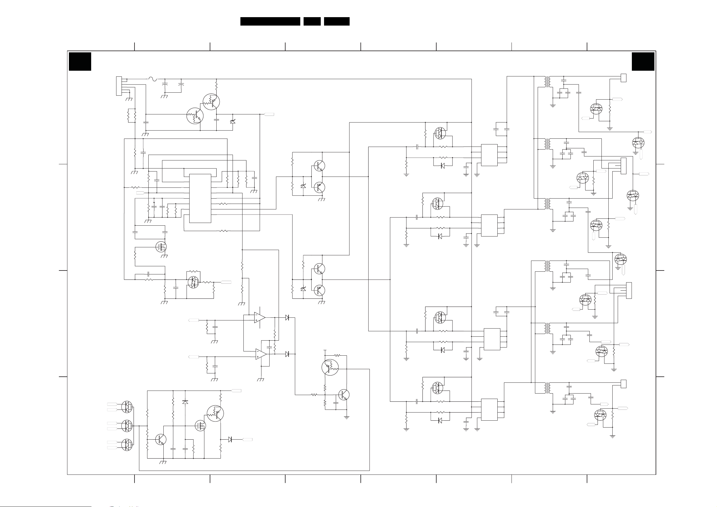
Inverter Panel
1
INVERTER
I I
D
C
B
A
O/S 1
O/S 2
O/S 3
O/S 4
O/S 5
O/S 6
Circuit Diagrams and PWB Layouts
2
CN1
1
2
3
4
5
6
R24
NC
D1/NC
BAW56K
D2/NC
BAW56K
D3/NC
BAW56K
R2 0
R4
5.6K
R5
47K
R12
100
F1
5A
U1
R61
510K
510K
Q1
DTC143
R23
R63
Q6
2N7002
R17
100(1206)
Q4
DTA143
C14
105
16
R20
15
100K
14
13
12
R21
11
22
10
R22
22
0
FB
R25
1K
C52
105
C55
105
R27
100
Q5
DTA143
D6
1N4148
R29
NC
C1
C3
220uF/25V
220uF/25V
C4
104
C5
105
R6
270K
C6
105
O/S
C8
C7
R7
20K
C9
331
C11
R11 3K
R15
100K
R1
300K
R3
100K
NC
681
103
R13
NC
R8
33kR916k
C10
NC
Q2
2N7002
R10
1M
R14
1M
Q3
2222
C13
105
1
2
3
4
5
6
7
8 9
R26
NC
D4
C12
104
BAV99
B
A
D5
1N4148
C34
R16
1M\NC
105
A K
IC-Vcc
8.2V
3
C15
103
LM393
IC-Vcc
R31
NC
ZD2
4.3V
R30
560
A K
R33
NC
ZD3
R32
4.3V
560
A K
U1B
LM393
U1A
C54
105
D26
1N4148
R28
3K
R62
3K
D25
1N4148
DTA143
R60
ZD1
R18
R19
100K
100K
R56
2K
R57
K
4.7
O/S
Q10
R58
10K
1K
R59
30K
D7
2222
Q7
2907
D8
2222
Q8
2907
VCC / 8.2V
41TCM1.0E LA 7.
54
D9
R34
22K
C16
223
R35
150
R36
22K
C17
223
R37
150
22K
C18
223
R39
10K
R64
Q11
C56
104
2222
150
R40
22K
C19
223
R41
150
BAW56K
R42 10
R43 10
D10 1N4148
D11
BAW56K
R44 10
R45
10
D12 1N4148
D13
R38
BAW56K
R46
10
R47 10
D14 1N4148
D15
BAW56K
10
R48
R49
10
D16 1 N4148
6
C25
C21
225(1206)
5
D2
6
D2
7
D1
8
D1
5
6
D2
7
D1
8
D1
C24
225(1206)
5
6
D2
7
D1
8
D1
5
6
D2
7
D1
8
D1
C20
225(1206)
U2
4
G2
3
S2
2
G1
1
3
2
1
S1
U3
G24D2
S2
G1
S1
C22
105
C23
105
225(1206)
U4
G24D2
3
S2
2
G1
1
3
2
1
S1
U5
G24D2
S2
G1
S1
C26
105
C27
105
7
T1
4
1
T2
4
1
T3
4
1
T4
4 7
1
T5
4 7
1
T6
4 7
1
8
R50
CN2
1
2
O/S 1
820
CN3
1
2
3
4
5
CON5
D
C
D23
BAV99
B
D
7
C28
10pF
6
C36
NC
C29
10pF
C37
471
BAV99
D17
FB
C39
C38
471
NC
C35
222
7
6
C53
222
D21
BAV99
O/S2
R54
820
FB
7
C30
10pF
6
C40
222
C31
10pF
6
C49
222
D19
BAV99
C32
10pF
6
C46
222
C33
10pF
6
C43
222
C42
BAV99
D22
BAV99
D20
D18
471
BAV99
FB
C51
471
R52
820
C48
471
FB
C45
471
O/S 4
O/S 3
R51
820
D
R53
820
C
R55
820
FB
C41
NC
C50
NC
FB
C47
NC
C44
NC
CN4
O/S 5
CN5
1
2
O/S 6
D24
B
BAV99
1
2
3
4
5
CON5
D27
A
BAV99
C
B
A
123 456 87
I_17930_035.eps
220408
Page 42
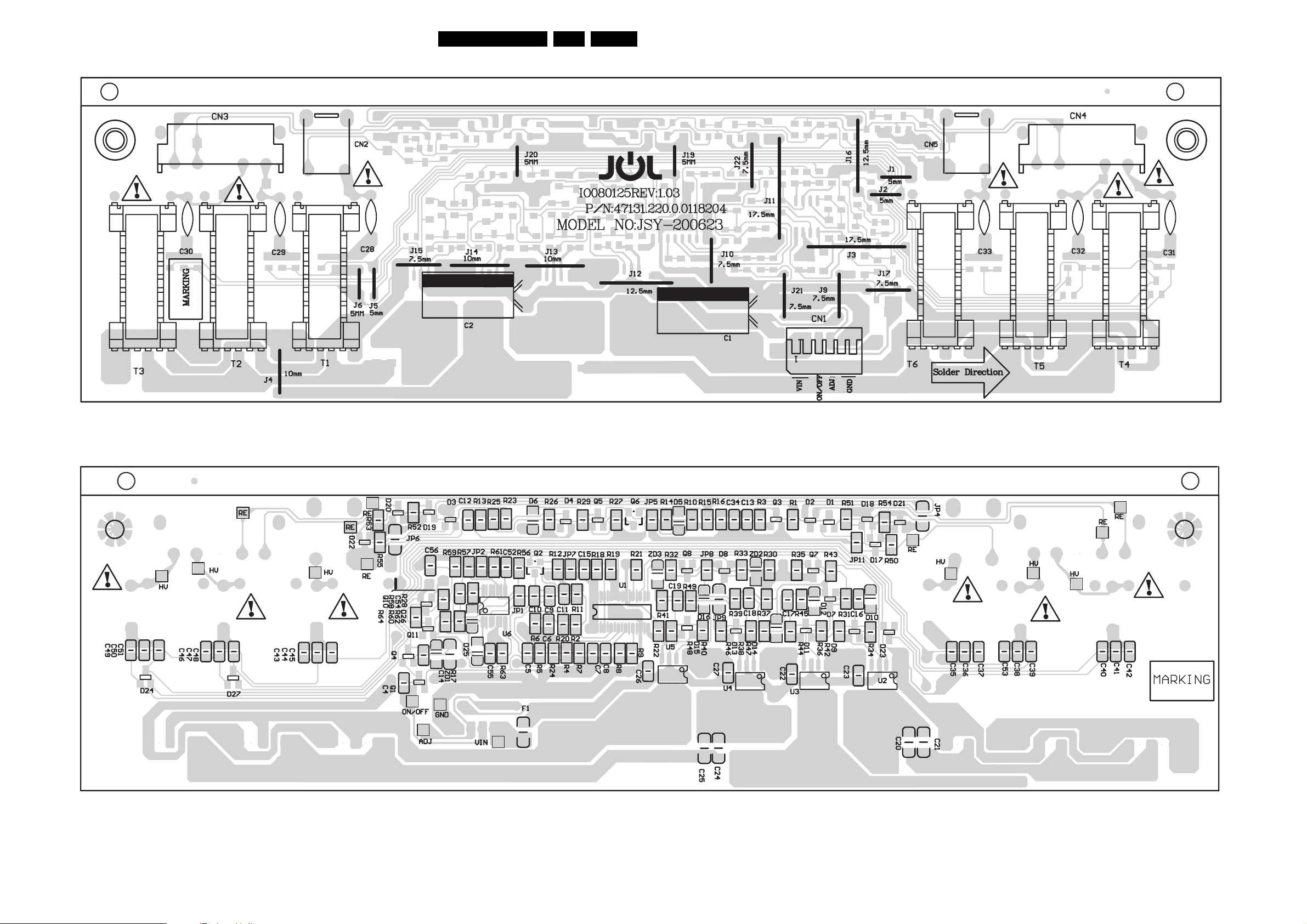
Circuit Diagrams and PWB Layouts
Layout Inverter Panel (Top Side)
42TCM1.0E LA 7.
Layout Inverter Panel (Bottom Side)
I_17930_036.eps
220408
I_17930_037.eps
220408
Page 43
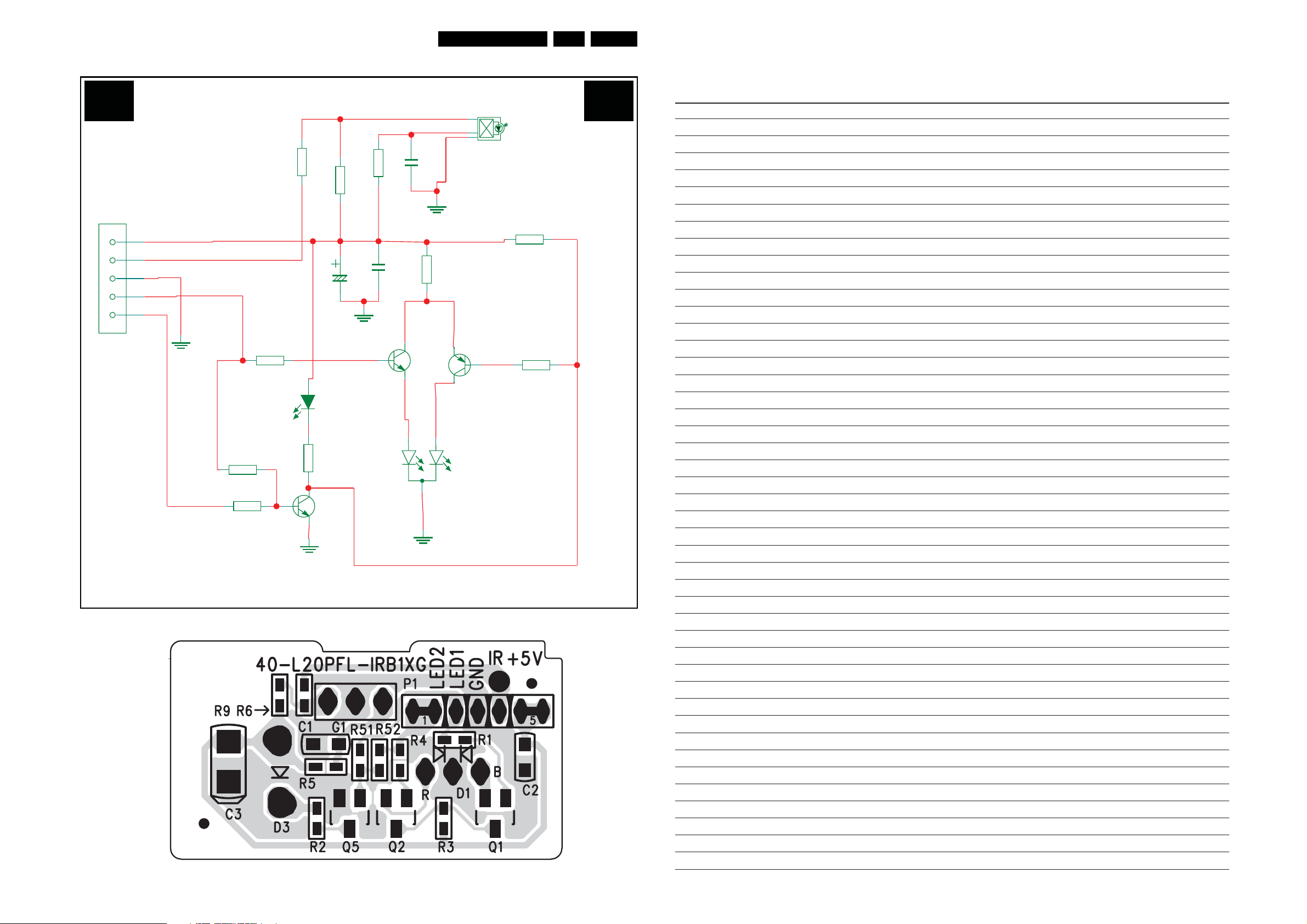
IR LED Panel
s
4
Circuit Diagrams and PWB Layouts
43TCM1.0E LA 7.
J J
P1
R6
100R
R9
GND
LED1
IR
+5V
R1
4K7
C3
47U
D3
5
4
3
2
1
LED2
4K7
6V3
R5
100R
C2
BT3904
C1
10U
R3
10U
1K
C
Q1
B
E
Q2
E
C
IR
VCC
GND
B
BT3906
G1
4K7
3K3
R7
R4
IR & LED
Personal Notes:
R51
4K7
R52
4K7
R2
B
BT3904
Layout IR LED Panel (Top Side)
4K7
C
E
Q5
13
RW
D1
2
I_17930_033.eps
220408
I_17930_034.eps
220408
E_06532_012.ep
13100
Page 44
Personal Notes:
Circuit Diagrams and PWB Layouts
44TCM1.0E LA 7.
E_06532_013.eps
131004
Page 45
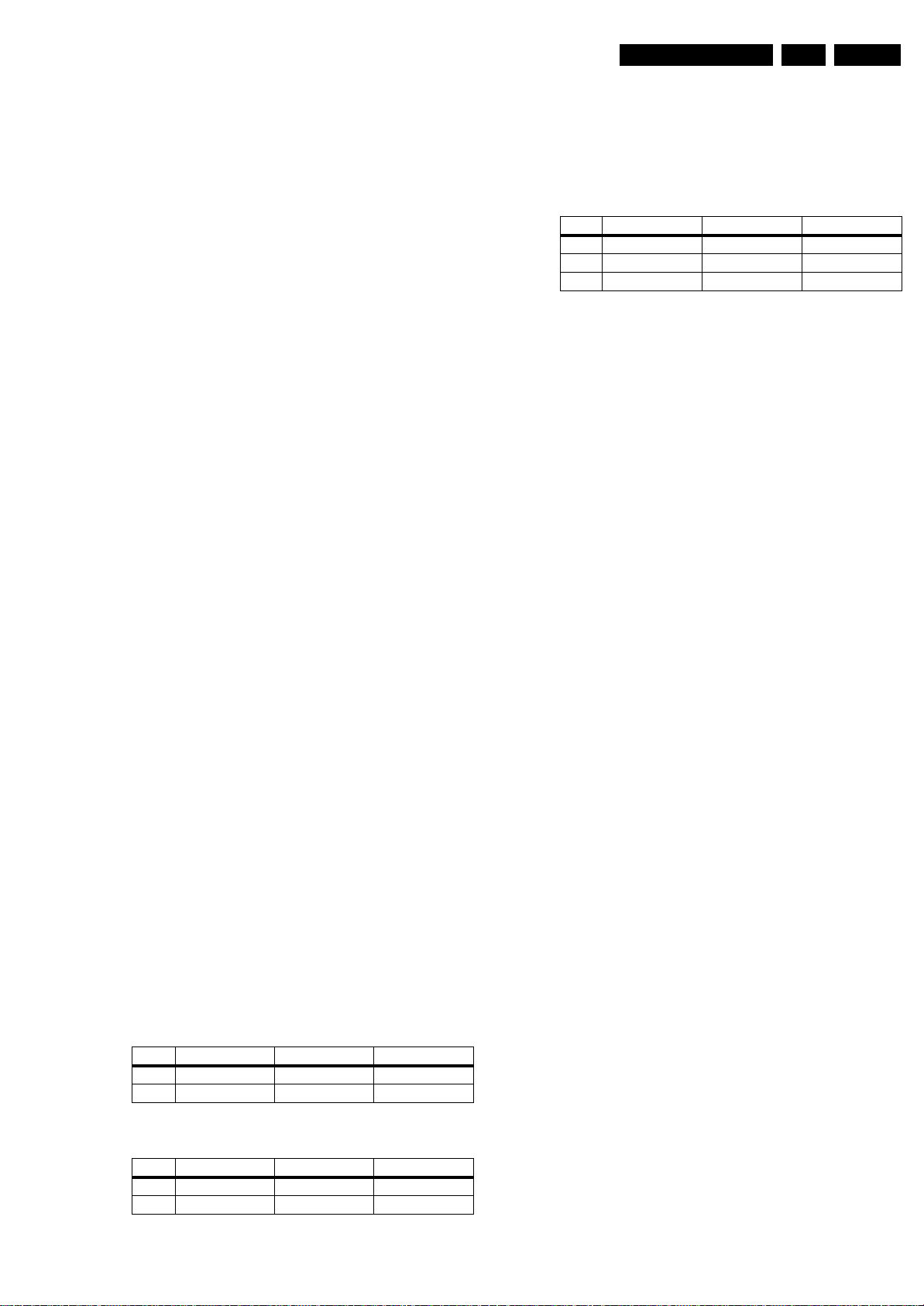
8. Alignments
Alignments
EN 45TCM1.0E LA 8.
Index of this chapter:
8.1 Electrical Alignments
8.2 Hardware Alignments
Note:
The Service Modes are described in chapter 5. Menu
navigation is done with the CURSOR UP, DOWN, LEFT or
RIGHT keys of the remote control transmitter.
8.1 Electrical Alignments
Perform all electrical adjustments under the following
conditions:
• Power supply voltage (depends on region):
– AP-NTSC: 120 VAC or 230 VAC / 50 Hz (± 10%).
– AP-PAL-multi: 120 - 230 VAC / 50 Hz (± 10%).
– EU: 230 VAC / 50 Hz (± 10%).
– LATAM-NTSC: 120 - 230 VAC / 50 Hz (± 10%).
– US: 120 VAC / 60 Hz (± 10%).
• Connect the set to the mains via an isolation transformer
with low internal resistance.
• Allow the set to warm up for approximately 60 minutes.
• Measure voltages and waveforms in relation to correct
ground (e.g. measure audio signals in relation to
AUDIO_GND).
Caution: It is not allowed to use heatsinks as ground.
• Test probe: R
• Use an isolated trimmer/screwdriver to perform
alignments.
> 10 MΩ, Ci < 20 pF.
i
If you do not have a Colour Analyser, the following R, G, and B
values are for your reference.
Table 8-3 Reference Value of R, G, and B
Normal (9300K) Cool (11500K) Warm (6500K)
R 146 136 154
G 146 141 150
B 146 152 138
8.2 Hardware Alignments
Not applicable.
8.2.1 White Balance Adjustment (VGA Mode)
Only VGA input requires color temperature adjustment as all
other inputs or relative ones. Both warm and cool colour
coordinates are also relatives to normal colour temperature
mode ones.
Equipment Requirements: Colour analyser.
Pre conditions:
• PicturePreset: Standard
• BlackExpand: Off
• PicturePreset: Standard
• Tone: Normal
• DynamicContrast Off
Colour Temp Alignment
Apply a 1366 × 768 /50Hz signal with white pattern, set
“brightness” at 100%, and “contrast” at 50%. Adjust the R, G,
and B Sub-Gain for the screen centre.
The 1931 CIE chromaticity (x, y) co-ordinates shall be:
Table 8-1 Alignment for 19" & 20" with a colour analyser
Normal (8 000K) Cool (9000K) Warm (65 00K)
x 0.296 +/- 0.010 0.289 +/- 0.010 0.314 +/- 0.010
y 0.299 +/- 0.010 0.291 +/- 0.010 0.319 +/- 0.010
Table 8-2 Alignment for 26" with a colour analyser
Normal (9000K) Cool (11000K) Warm (6500K)
x 0.289 +/- 0.010 0.278 +/- 0.010 0.314 +/- 0.010
y 0.291 +/- 0.010 0.278 +/- 0.010 0.319 +/- 0.010
Page 46
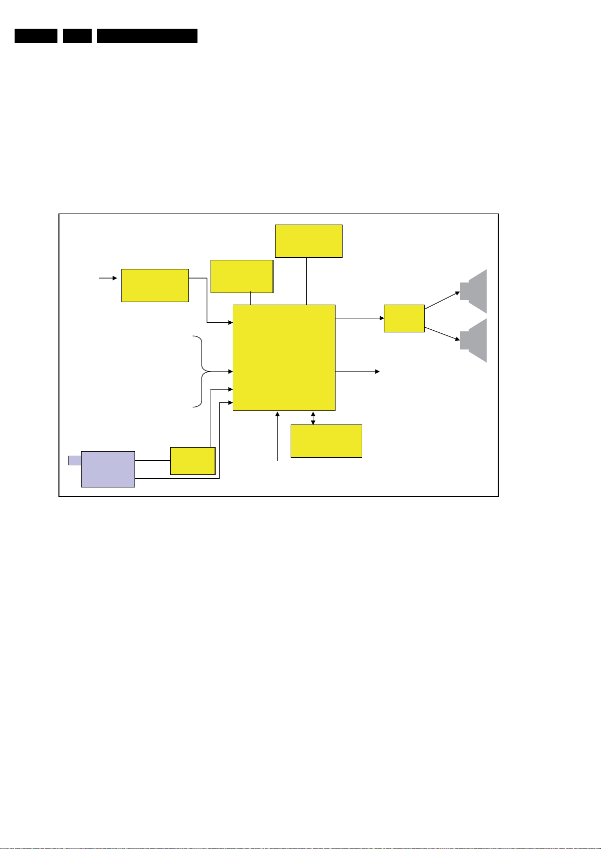
EN 46 TCM1.0E LA9.
Circuit Descriptions, Abbreviation List, and IC Data Sheets
9. Circuit Descriptions, Abbreviation List, and IC Data Sheets
Index of this chapter:
9.1 Introduction
9.2 Abbreviation List
9.3 IC Data Sheets
Notes:
•Only new circuits (circuits that are not published recently)
are described.
• Figures can deviate slightly from the actual situation, due
to different set executions.
Flash
HDMI
HDMI 1.2 Rx
S29AL016D
MT8293
•
CVBS
• YPbPr
• VGA w audio
• 1 Scart
(RGB + CVBS + Monitor out)
• Headphone
Main Processor
9.1 Introduction
This chassis supports PC analogue input up to WXGA
resolution, and supports TV (RF) for Europe systems: PAL B/
G, PAL D/K, PAL I, SECAM B/G, SECAM D/K, CVBS, HDMI
and VGA signal input.
The platform is also designed for the lowest power
consumption in off/stand-by mode (<0.3W) to fulfil new Philips
CE environment policy requirement.
SDR RAM
K4S641632K
Audio
Amp
MT8200
LVDS
SIFCVBS
Video
Tuner
It uses one main ICs: MT8200ATE (One Chip LCD-TV
Controller).
The MT8200ATE is a highly integrated single chip for LCD TV
supporting video input and output format up to HDTV. It
includes 3D comb filter TV decoder to retrieve the best image
from popular composite signals. Embedded HDTV/VGA
decoders let the high bandwidth input signals perfectly
reproduced.
The 16/8 bits digital port may accept CCIR-656/601 external
digital input video source. New 2
motion adaptive de-interlacer converts accordingly the
interlace video into progressive one with overlay of a 2D
Graphic processor. It incorporates advanced full function
colour processing with fully 10-bit path provides high quality
video contents.
Its on-chip audio processor decodes analog signals from tuner
with lip sync control, delivering high quality post-processed
sound effect to customers.
The on-chip microprocessor reduces the system BOM and
shortens the schedule of UI design by high level C program.
Demod
nd
generation advanced
IR, Control knobs
Figure 9-1 Set functional diagram
Standby MCU
NEC
I_17930_066.eps
240408
The CM2021 HDMI Receiver Port Protection and Interface
Device is specifically designed for next generation HDMI Host
interface protection. An integrated package provides all ESD,
level shift and backdrive protection for an HDMI port in a single
38-Pin TSSOP package.
The MT8200 is surrounded by a tuner, a video demodulator, a
HDMI interface, SDR and flash memory, an audio amplifier,
and optionally a stand-by microprocessor (26"). For the smaller
set versions also the inverter board is serviceable.
Page 47
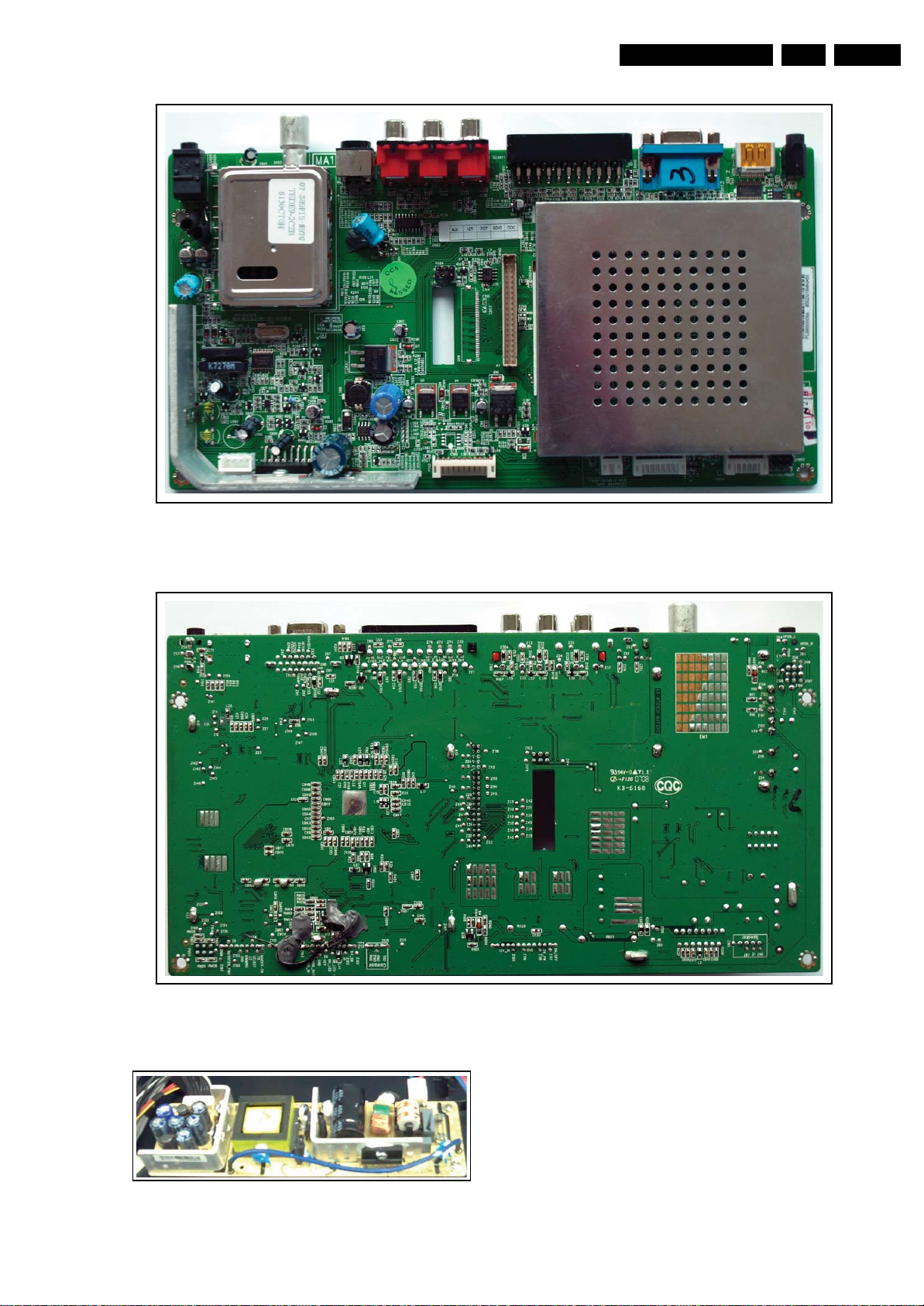
Circuit Descriptions, Abbreviation List, and IC Data Sheets
EN 47TCM1.0E LA 9.
Figure 9-2 SSB front
I_17930_049.eps
240408
Figure 9-4 Power supply unit (20")
Figure 9-3 SSB back
I_17930_067.eps
240408
I_17930_050.eps
240408
Page 48
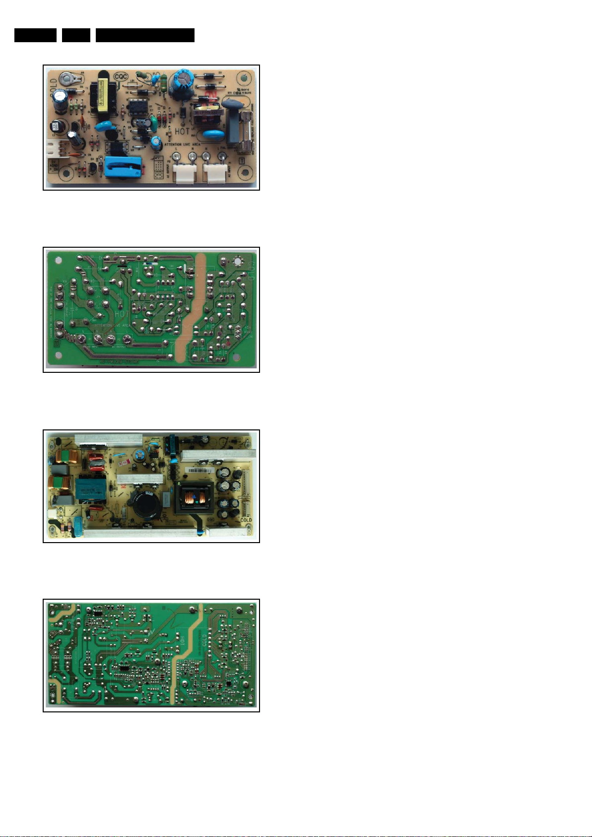
EN 48 TCM1.0E LA9.
Figure 9-5 Stand-by power supply unit front (26")
Figure 9-6 Stand-by power supply unit back (26")
Figure 9-7 Power supply unit front (26")
Figure 9-8 Power supply unit back (26")
Circuit Descriptions, Abbreviation List, and IC Data Sheets
9.2 Abbreviation List
0/6/12 SCART switch control signal on A/V
board. 0 = loop through (AUX to TV),
6 = play 16 : 9 format, 12 = play 4 : 3
format
1080i 1080 visible lines, interlaced
1080p 1080 visible lines, progressive scan
2DNR Spatial (2D) Noise Reduction
3DNR Temporal (3D) Noise Reduction
I_17930_051.eps
240408
I_17930_052.eps
240408
I_17930_053.eps
240408
I_17930_054.eps
240408
AARA Automatic Aspect Ratio Adaptation:
ACI Automatic Channel Installation:
ADC Analogue to Digital Converter
AFC Automatic Frequency Control: control
AGC Automatic Gain Control: algorithm that
AM Amplitude Modulation
ANR Automatic Noise Reduction: one of the
AP Asia Pacific
AR Aspect Ratio: 4 by 3 or 16 by 9
ASF Auto Screen Fit: algorithm that adapts
ATSC Advanced Television Systems
ATV See Auto TV
Auto TV A hardware and software control
AV External Audio Video
AVC Audio Video Controller
AVIP Audio Video Input Processor
B/G Monochrome TV system. Sound
BLR Board-Level Repair
BTSC Broadcast Television Standard
B-TXT Blue TeleteXT
C Centre channel (audio)
CEC Consumer Electronics Control bus:
CL Constant Level: audio output to
CLR Component Level Repair
COLUMBUS COlor LUMinance Baseband
ComPair Computer aided rePair
CP Connected Planet / Copy Protection
CSM Customer Service Mode
CTI Color Transient Improvement:
CVBS Composite Video Blanking and
DAC Digital to Analogue Converter
DBE Dynamic Bass Enhancement: extra
algorithm that adapts aspect ratio to
remove horizontal black bars; keeps
the original aspect ratio
algorithm that installs TV channels
directly from a cable network by
means of a predefined TXT page
signal used to tune to the correct
frequency
controls the video input of the feature
box
algorithms of Auto TV
aspect ratio to remove horizontal black
bars without discarding video
information
Committee, the digital TV standard in
the USA
system that measures picture content,
and adapts image parameters in a
dynamic way
carrier distance is 5.5 MHz
Committee. Multiplex FM stereo sound
system, originating from the USA and
used e.g. in LATAM and AP-NTSC
countries
remote control bus on HDMI
connections
connect with an external amplifier
Universal Sub-system
manipulates steepness of chroma
transients
Synchronization
low frequency amplification
Page 49

Circuit Descriptions, Abbreviation List, and IC Data Sheets
EN 49TCM1.0E LA 9.
DDC See “E-DDC”
D/K Monochrome TV system. Sound
carrier distance is 6.5 MHz
DFI Dynamic Frame Insertion
DFU Directions For Use: owner's manual
DMR Digital Media Reader: card reader
DMSD Digital Multi Standard Decoding
DNM Digital Natural Motion
DNR Digital Noise Reduction: noise
reduction feature of the set
DRAM Dynamic RAM
DRM Digital Rights Management
DSP Digital Signal Processing
DST Dealer Service Tool: special remote
control designed for service
technicians
DTCP Digital Transmission Content
Protection; A protocol for protecting
digital audio/video content that is
traversing a high speed serial bus,
such as IEEE-1394
DVB-C Digital Video Broadcast - Cable
DVB-T Digital Video Broadcast - Terrestrial
DVD Digital Versatile Disc
DVI(-d) Digital Visual Interface (d= digital only)
E-DDC Enhanced Display Data Channel
(VESA standard for communication
channel and display). Using E-DDC,
the video source can read the EDID
information form the display.
EDID Extended Display Identification Data
(VESA standard)
EEPROM Electrically Erasable and
Programmable Read Only Memory
EMI Electro Magnetic Interference
EPLD Erasable Programmable Logic Device
EU Europe
EXT EXTernal (source), entering the set by
SCART or by cinches (jacks)
FBL Fast BLanking: DC signal
accompanying RGB signals
FDS Full Dual Screen (same as FDW)
FDW Full Dual Window (same as FDS)
FLASH FLASH memory
FM Field Memory or Frequency
Modulation
FPGA Field-Programmable Gate Array
FTV Flat TeleVision
Gb/s Giga bits per second
G-TXT Green TeleteXT
H H_sync to the module
HD High Definition
HDD Hard Disk Drive
HDCP High-bandwidth Digital Content
Protection: A “key” encoded into the
HDMI/DVI signal that prevents video
data piracy. If a source is HDCP coded
and connected via HDMI/DVI without
the proper HDCP decoding, the
picture is put into a “snow vision” mode
or changed to a low resolution. For
normal content distribution the source
and the display device must be
enabled for HDCP “software key”
decoding.
HDMI High Definition Multimedia Interface
HP HeadPhone
I Monochrome TV system. Sound
2
I
C Inter IC bus
2
I
D Inter IC Data bus
2
I
S Inter IC Sound bus
carrier distance is 6.0 MHz
IF Intermediate Frequency
Interlaced Scan mode where two fields are used
to form one frame. Each field contains
half the number of the total amount of
lines. The fields are written in “pairs”,
causing line flicker.
IR Infra Red
IRQ Interrupt Request
ITU-656 The ITU Radio communication Sector
(ITU-R) is a standards body
subcommittee of the International
Telecommunication Union relating to
radio communication. ITU-656 (a.k.a.
SDI), is a digitized video format used
for broadcast grade video.
Uncompressed digital component or
digital composite signals can be used.
The SDI signal is self-synchronizing,
uses 8 bit or 10 bit data words, and has
a maximum data rate of 270 Mbit/s,
with a minimum bandwidth of 135
MHz.
ITV Institutional TeleVision; TV sets for
hotels, hospitals etc.
JOP Jaguar Output Processor
LS Last Status; The settings last chosen
by the customer and read and stored
in RAM or in the NVM. They are called
at start-up of the set to configure it
according to the customer's
preferences
LATAM Latin America
LCD Liquid Crystal Display
LED Light Emitting Diode
L/L' Monochrome TV system. Sound
carrier distance is 6.5 MHz. L' is Band
I, L is all bands except for Band I
LORE LOcal REgression approximation
noise reduction
LPL LG.Philips LCD (supplier)
LS Loudspeaker
LVDS Low Voltage Differential Signalling
Mbps Mega bits per second
M/N Monochrome TV system. Sound
carrier distance is 4.5 MHz
MIPS Microprocessor without Interlocked
Pipeline-Stages; A RISC-based
microprocessor
MOP Matrix Output Processor
MOSFET Metal Oxide Silicon Field Effect
Transistor, switching device
MPEG Motion Pictures Experts Group
MPIF Multi Platform InterFace
MUTE MUTE Line
NC Not Connected
NICAM Near Instantaneous Compounded
Audio Multiplexing. This is a digital
sound system, mainly used in Europe.
NTC Negative Temperature Coefficient,
non-linear resistor
NTSC National Television Standard
Committee. Color system mainly used
in North America and Japan. Color
carrier NTSC M/N= 3.579545 MHz,
NTSC 4.43= 4.433619 MHz (this is a
VCR norm, it is not transmitted off-air)
NVM Non-Volatile Memory: IC containing
TV related data such as alignments
O/C Open Circuit
OSD On Screen Display
OTC On screen display Teletext and
Control; also called Artistic (SAA5800)
P50 Project 50: communication protocol
between TV and peripherals
PAL Phase Alternating Line. Color system
mainly used in West Europe (color
carrier= 4.433619 MHz) and South
America (color carrier PAL M=
Page 50

EN 50 TCM1.0E LA9.
Circuit Descriptions, Abbreviation List, and IC Data Sheets
3.575612 MHz and PAL N= 3.582056
MHz)
PCB Printed Circuit Board (same as “PWB”)
PCM Pulse Code Modulation
PDP Plasma Display Panel
PFC Power Factor Corrector (or Pre-
conditioner)
PIP Picture In Picture
PLL Phase Locked Loop. Used for e.g.
FST tuning systems. The customer
can give directly the desired frequency
POR Power On Reset, signal to reset the uP
Progressive Scan Scan mode where all scan lines are
displayed in one frame at the same
time, creating a double vertical
resolution.
PTC Positive Temperature Coefficient,
non-linear resistor
PWB Printed Wiring Board (same as “PCB”)
PWM Pulse Width Modulation
QRC Quasi Resonant Converter
QTNR Quality Temporal Noise Reduction
QVCP Quality Video Composition Processor
RAM Random Access Memory
RGB Red, Green, and Blue. The primary
color signals for TV. By mixing levels
of R, G, and B, all colors (Y/C) are
reproduced.
RC Remote Control
RC5 / RC6 Signal protocol from the remote
control receiver
RESET RESET signal
ROM Read Only Memory
R-TXT Red TeleteXT
SAM Service Alignment Mode
S/C Short Circuit
SCART Syndicat des Constructeurs
d'Appareils Radiorécepteurs et
Téléviseurs
SCL Serial Clock I
SCL-F CLock Signal on Fast I
SD Standard Definition
SDA Serial Data I
SDA-F DAta Signal on Fast I
2
C
2
C
2
C bus
2
C bus
SDI Serial Digital Interface, see “ITU-656”
SDRAM Synchronous DRAM
SECAM SEequence Couleur Avec Mémoire.
Color system mainly used in France
and East Europe. Color carriers=
4.406250 MHz and 4.250000 MHz
SIF Sound Intermediate Frequency
SMPS Switched Mode Power Supply
SoC System on Chip
SOG Sync On Green
SOPS Self Oscillating Power Supply
S/PDIF Sony Philips Digital InterFace
SRAM Static RAM
SRP Service Reference Protocol
SSB Small Signal Board
STBY STand-BY
SVGA 800x600 (4:3)
SVHS Super Video Home System
SW Software
SWAN Spatial temporal Weighted Averaging
Noise reduction
SXGA 1280x1024
TFT Thin Film Transistor
THD Total Harmonic Distortion
TMDS Transmission Minimized Differential
Signalling
TXT TeleteXT
TXT-DW Dual Window with TeleteXT
UI User Interface
uP Microprocessor
UXGA 1600x1200 (4:3)
V V-sync to the module
VCR Video Cassette Recorder
VESA Video Electronics Standards
Association
VGA 640x480 (4:3)
VL Variable Level out: processed audio
output toward external amplifier
VSB Vestigial Side Band; modulation
method
WYSIWYR What You See Is What You Record:
record selection that follows main
picture and sound
WXGA 1280x768 (15:9)
XTAL Quartz crystal
XGA 1024x768 (4:3)
Y Luminance signal
Y/C Luminance (Y) and Chrominance (C)
signal
YPbPr Component video. Luminance and
scaled color difference signals (B-Y
and R-Y)
YUV Component video
Page 51
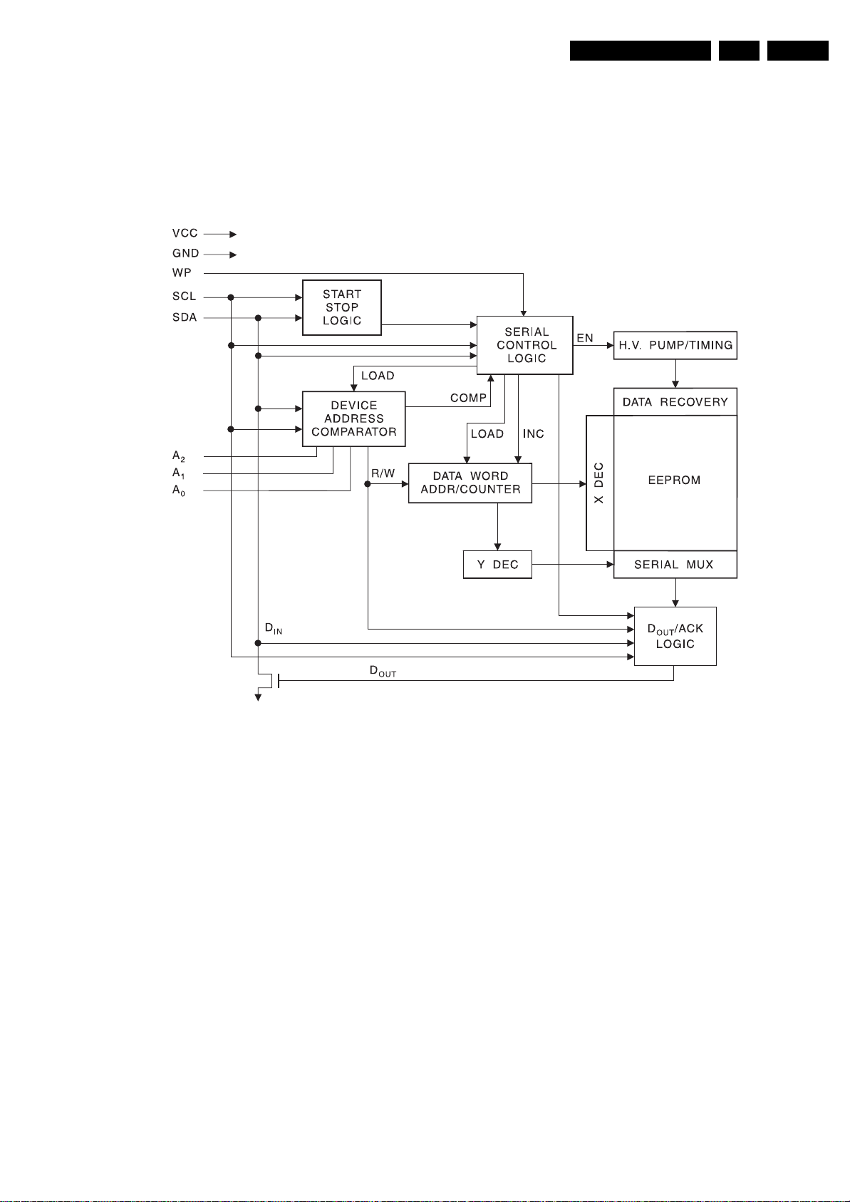
Circuit Descriptions, Abbreviation List, and IC Data Sheets
9.3 IC Data Sheets
This section shows the internal block diagrams and pin layouts
of ICs that are drawn as "black boxes" in the electrical diagrams
(with the exception of "memory" and "logic" ICs).
9.3.1 Diagram B, AT24C02B
EN 51TCM1.0E LA 9.
Figure 9-9 Block diagram
I_17930_069.eps
250408
Page 52
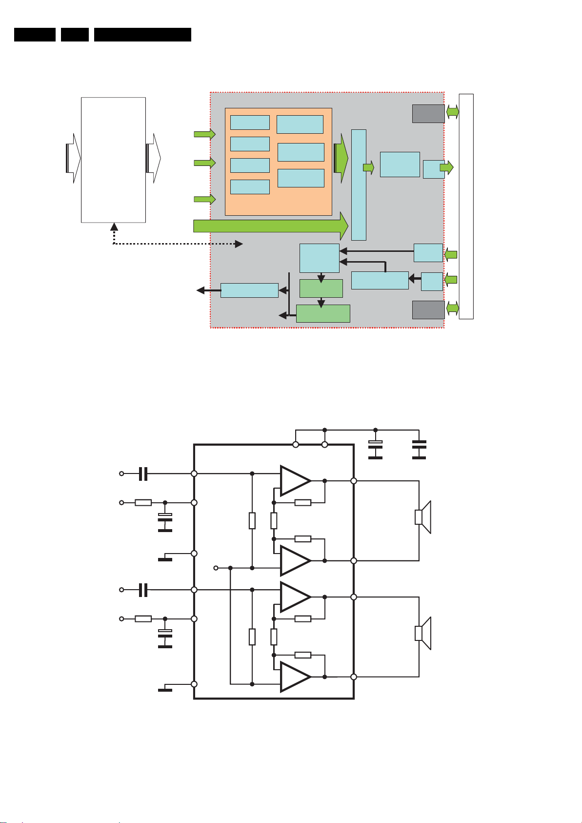
EN 52 TCM1.0E LA9.
A
9.3.2 Diagram B, MT8200
Circuit Descriptions, Abbreviation List, and IC Data Sheets
(Customer)
External
Switches
Control Signal (GPIO, …)
9.3.3 Diagram B, TDA7266
CVBS / SV
(x8)
YPbPr
VG
(aRGB
Digital
TTL
Analog Front End
ADC
ADC
TVD
HDTVD
ADC
VGAD
ADC
)
Analog Path
Digital Path
TTL Tx
Figure 9-10 Block diagram
OSD
Merge
Gamma
Dithering
MDDi
MUX
Color Proc
8032
DS
DRAM
OSD
US
DSP
I_17930_070.eps
250408
IN1
IN2
0.22µF
0.22µF
S-GND
PW-GND
4
7YB-TS
9
12
6ETUM
8
Vref
V
CC
133
+
-
-
+
+
-
-
+
1
2
15
14
470µF100nF
OUT1+
OUT1-
OUT2+
OUT2-
I_17930_071.eps
250408
Figure 9-11 Block diagram
Page 53
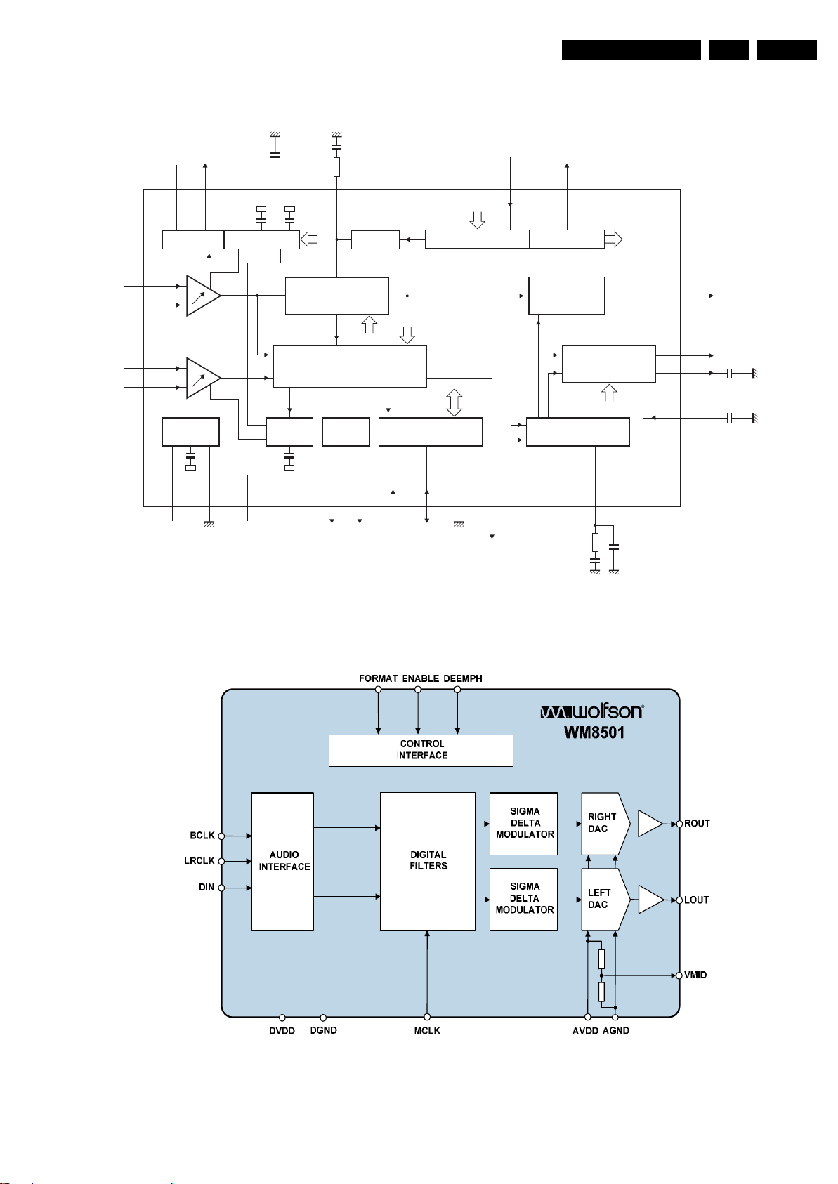
Circuit Descriptions, Abbreviation List, and IC Data Sheets
9.3.4 Diagram B, TDA9886
TOP
TAGC
14 (15)
C
AGC(neg)
TUNER AGC
VIF2
2 (31)
1 (30)
VIF1
SIF2
24 (27)
23 (26)
SIF1
SUPPLY
18 (20)20 (22)
V
P
(1) Not connected for TDA9885.
Pin numbers for TDA9885HN and TDA9886HN in parenthesis.
C
VAGC(pos)
VIF-AGC
(1)
VAGC
C
BL
VIF-PLL
SINGLE REFERENCE QSS MIXER
INTERCARRIER MIXER
AND AM DEMODULATOR
SIF-AGC
(6, 12, 13, 14, 17,
19, 25, 28, 29, 32)
13
n.c.AGND
OUTPUT
C
AGC
VIF-PLL
VPLL
19 (21) )32( 12)61( 51)71( 61)8( 9
PORTS
filter
RC VCO
22 (24)3 (1)
DIGITAL VCO CONTROL AFC DETECTOR
TDA9885
TDA9886
MAD
2
I
C-BUS TRANSCEIVER
11 (10)
sound intercarrier output
external reference signal
or 4 MHz crystal
REF AFC
12 (11)
7 (5)
SIOMADSDASCL
DGND
and MAD select
SOUND CARRIER
TRAPS
4.5 to 6.5 MHz
AUDIO PROCESSING
AND SWITCHES
NARROW-BAND
FM-PLL DEMODULATOR
4 (2)10 (9)
LLPMF2PO1PO
FM-PLL
filter
(18) 17
(7) 8
(3) 5
(4) 6
CVBS
AUD
DEEM
AFD
EN 53TCM1.0E LA 9.
video output: 2 V (p-p)
[1.1 V (p-p) without trap]
audio output
de-emphasis
network
C
AF
I_17930_072.eps
250408
9.3.5 Diagram B, WM8501
Figure 9-12 Block diagram
Figure 9-13 Block diagram
I_17930_073.eps
250408
Page 54
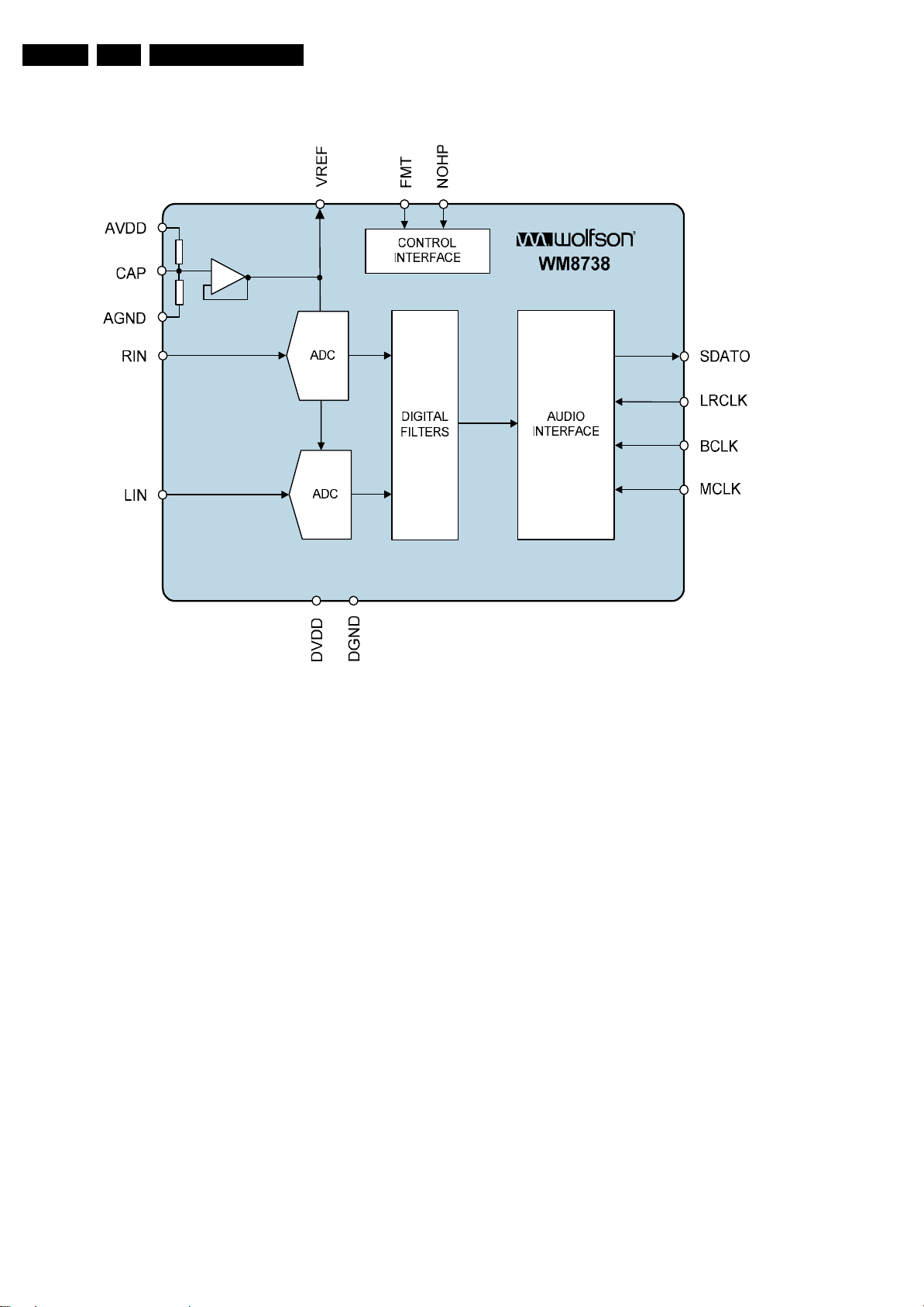
EN 54 TCM1.0E LA9.
9.3.6 Diagram B, WM8738
Circuit Descriptions, Abbreviation List, and IC Data Sheets
Figure 9-14 Block diagram
I_17930_074.eps
250408
Page 55
Spare Parts List & CTN Overview
10. Spare Parts List & CTN Overview
For the latest spare part overview, please consult the Philips
Service website.
Table 10-1 Sets described in this manual:
CTN Styling Published in:
19PFL3403/60 MG8 3122 785 17931
19PFL3403S/60 MG8 3122 785 17931
20PFL3403/10 MG8 3122 785 17930
20PFL3403/60 MG8 3122 785 17931
22PFL3403/60 MG8 3122 785 17931
26PFL3403/10 MG8 3122 785 17930
26PFL3403/60 MG8 3122 785 17931
11. Revision List
Manual xxxx xxx xxxx.0
• First release.
Manual xxxx xxx xxxx.1
• All Chapters: Russian sets (/60) added.
• Chapter 5: ComPair/UART cables: 12nc and descriptions
updated.
• Chapter 9: Abbreviation list updated.
EN 55TCM1.0E LA 10.
 Loading...