

PJDLC05C-05
Fig.21
VOLTAGE
5.0 Volts
POWER
400 Watts
ULTRA LOW CAPACITANCE DUAL TRANSIET VOLTAGE
SUPPRESSOR FOR HIGH SPEED DATA LINES
This transient overvoltage suppressor is intended to protect sensitive
equipment against electrostatic discharge events as well to offer a
minimum insertion loss in data transmission lines in communications ports
used in portable consumer, computing and networking applications. This
dual transient voltage suppressor comes in a single SOT-23, offering
board space reduction, where the application requires it.
This device comes with two pairs of high speed switching diodes
connected in series, where both pairs are electrically isolated, offering a
very low capacitance, minimizing the insertion losses in data transmission
lines.
FEATURES
• Maximum capacitance @ 0 Vdc Bias of 1.0 pF between terminals 1-3
or terminals 2-3
• IEC61000-4-2 esd 15kV Air, 8kV contact compliance
• Lead free in comply with EU RoHS 2002/95/EC directives.
• Green molding compound as per IEC61249 Std. . (Halogen Free)
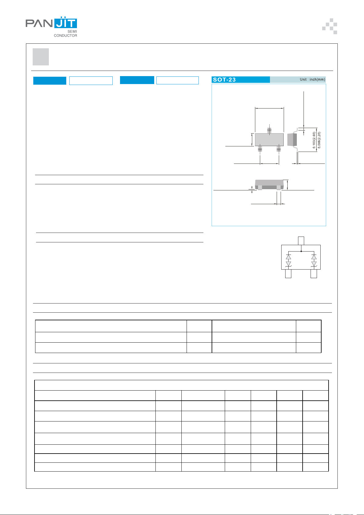
MECHANICAL DATA
• Case: SOT-23, plastic
• Terminals: solderable per MIL-STD-750, Method 2026
• Approx. Weight: 0.0003 ounces, 0.0084 grams
• Marking : DEA
0.056(1.40)
0.047(1.20)
0.079(2.00)
0.070(1.80)
0.004(0.10)MAX.
0.120(3.04)
0.110(2.80)
0.006(0.15)MIN.
0.008(0.20)
0.003(0.08)
0.044(1.10)
0.035(0.90)
0.020(0.50)
0.013(0.35)
3
1 2
MAXIMUM RATINGS
Parameter Symbol Value Units
Operating Junction T
Storage Temperature Range T
ELECTRICAL CHARACTERISTICS
PJDLC05C-05
Pa rame ter Symbo l Co nditions Mi nimum Typic al Maximum Units
Reverse Stand-Off Voltage V
Reverse Breakdown Voltage V
Reverse Leakage Current I
Junction Capacitance C
Peak Pulse Current I
Clamping Voltage V
Clamping Voltage V
RWM
BR
R
J
PP
C
C
V
Betwee n pi n1.2 to 3
V
R
t P=8/20 μsec - - 17 A
t P=8/20 μsec @1A - - 9.5 V
t P=8/20 μsec @5A - - 12 V
O
C
O
C
STG
J
-55 to +150
-55 to +150
---5V
I T=1mA 6 - - V
= 5V,
RWM
O
C
T = 25
=0V,f=1MHz
-0.81.2μA
--1.0pF
February 16,2011-REV.03
PAGE . 1
PJDLC05C-05
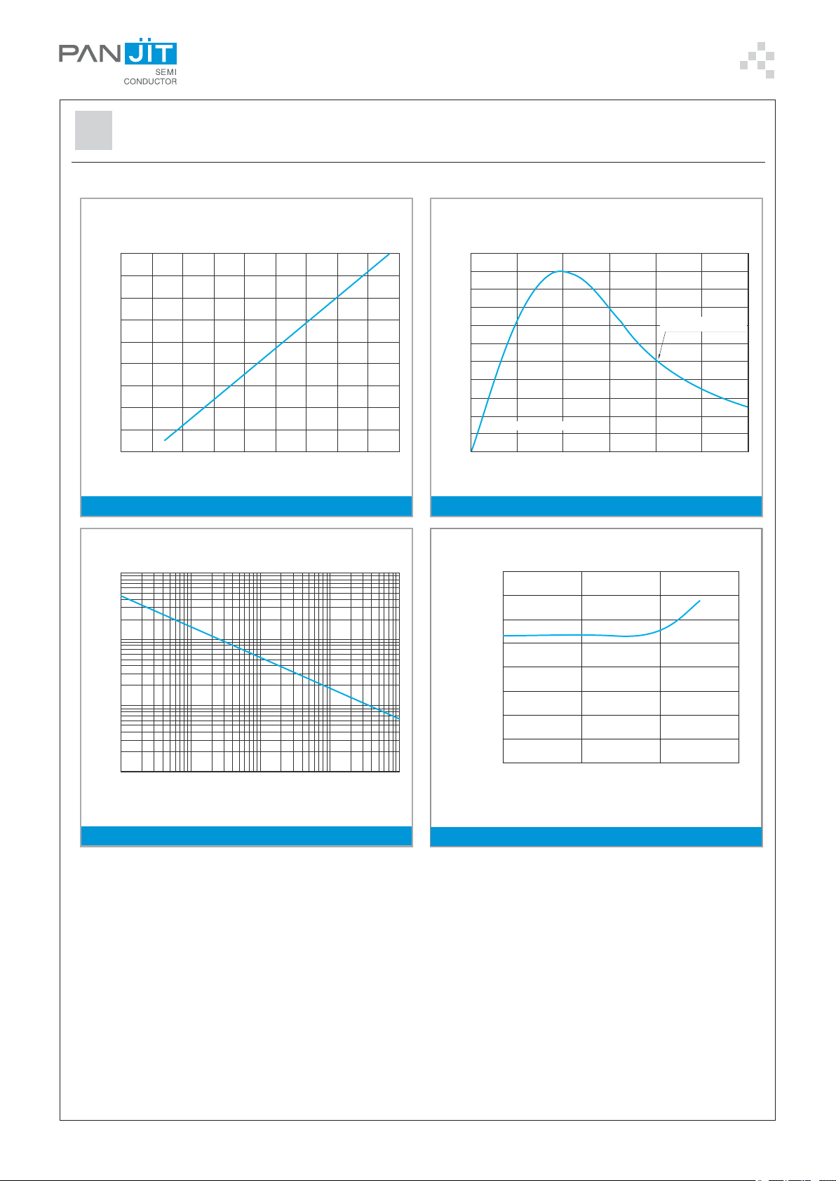
Fig 1- Clamping Voltage vs Ipp x sec820
FIG.4- TYPICAL JUNCTION CAPACITANCE UNDER BIAS
18
16
14
12
10
8
6
4
2
820 ,x sec Peak Current Amps
0
10
1
110
100
90
80
70
60
50
40
Percent of Ipp
30
20
Rise time s10-90% - 8m
10
0
6
8110
12
14
2418 20 2216
01015202530
Clamping Voltage Volts,
Fig 1- Clamping Voltage vs Ipp x sec820
5
time sec, m
Fig 2- Pulse Waveform
50% @20of Ipp sm
0.80
0.70
0.60
,pF
J
0.50
0.1
Peak Pulse Power kW,
0.01
0.1
10
Pulse Duration,msec
Fig 3- Non Repetitive Peak Pulse Power vs Pulse Time-
100
1000
0.40
0.30
0.20
0.10
Capacitance C
0.00
0246
Reverse Bias Voltage, V
FIG.4- TYPICAL JUNCTION CAPACITANCE UNDER BIAS
Power Derating Curve
February 16,2011-REV.03
PAGE . 2

PJDLC05C-05
MOUNTING PAD LAYOUT
SOT-23
0.035 MIN.
(0.90) MIN.
0.043
(1.10)
0.106
(2.70)
0.031 MIN.
(0.80) MIN.
0.037
(0.95)
Unit inch(mm):
0.043
(1.10)
0.078
(2.00)
ORDER INFORMATION
•
Packing information
T/R - 12K per 13" plastic Reel
T/R - 3K per 7” plastic Reel
LEGAL STATEMENT
Copyright PanJit International, Inc 2012
The information presented in this document is believed to be accurate and reliable. The specifications and information herein are
subject to change without notice. Pan Jit makes no warranty, representation or guarantee regarding the suitability of its produ cts for
any particular purpose. Pan Jit products are not authorized for use in life support devices or systems. Pan Jit does not convey any
license under its patent rights or rights of others.
February 16,2011-REV.03
PAGE . 3

PJDLC05C-05
For example :
RB500V-40_R2_
Part No.
00001
Serial number
Version code means HF
Packing size code means 13"
Packing type means T/R
Part No_packing code_Version
PJDLC05C-05_R1_00001
PJDLC05C-05_R1_10001
PJDLC05C-05_R2_00001
PJDLC05C-05_R2_10001
Packing Code XX Version Code XXXXX
Packing
type
1st Code
Packing size
code
2nd Code
HF or RoHS
1st Code 2nd~5th Code
T/B A N/A 0 HF 0 serial number
T/R R 7" 1 RoHS 1 serial number
B/P B 13" 2
T/P T 26mm X
TRR S 52mm Y
TRL L PBCU U
FORMING F PBCD D
February 16,2011-REV.03
PAGE . 4

 Loading...