

Panjit PJDLC05C-03 Schematic [ru]
PJDLC05C-03
Fig.21
VOLTAGE
5 V olts
POWER
250 Watts
ULTRA LOW CAPACIT ANCE DUAL TRANSIET VOL TAGE
SUPPRESSOR FOR HIGH SPEED DA T A LINES
This transient overvoltage suppressor is intended to protect sensitive
equipment against electrostatic discharge events as well to offer a
minimum insertion loss in data transmission lines in communications ports
used in portable consumer, computing and networking applications. This
dual transient voltage suppressor comes in a single SOT-23, offering
board space reduction, where the application requires it.
This device comes with two pairs of high speed switching diodes
connected in series, where both pairs are electrically isolated, offering a
very low capacitance, minimizing the insertion losses in data transmission
lines.
FEA TURES
• Maximum capacitance @ 0 Vdc Bias of 1pF between terminals 1-3
or terminals 2-3
• IEC61000-4-2 esd 15kV Air, 8kV contact compliance
• Lead free in comply with EU RoHS 2011/65/EU directives
• Green molding compound as per IEC61249 Std. . (Halogen Free)
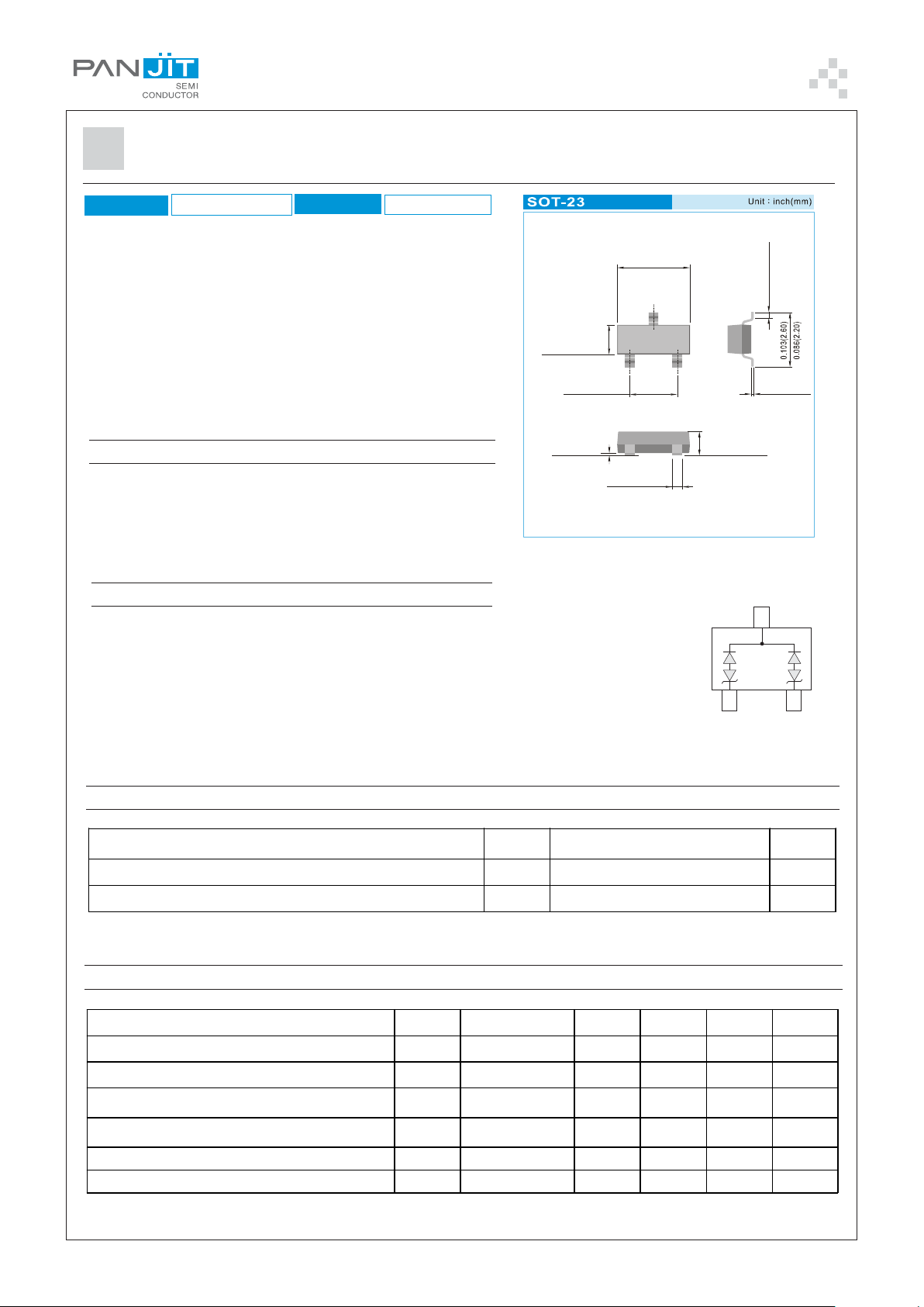
MECHANICAL DAT A
• Case: SOT-23, plastic
• Terminals: solderable per MIL-STD-750, Method 2026
• Approx. Weight: 0.0003 ounces, 0.008 grams
• Marking: DBA
0.056(1.40)
0.047(1.20)
0.079(2.00)
0.070(1.80)
0.004(0.10)
0.000(0.00)
0.120(3.04)
0.110(2.80)
0.020(0.50)
0.013(0.35)
0.044(1.10)
0.035(0.90)
0.006(0.15)MIN.
0.008(0.20)
0.003(0.08)
MAXIMUM RA TINGS
Parameter Symbol Value Units
Operating Junction T
Storage Temperature Range T
ELECTRICAL CHARACTERISTICS
Parameter Symbol Conditions Minimum Typical Maximum Units
Reverse Stand-Off Voltage V
Reverse Breakdown Voltage V
Reverse Leakage Current I
Junction Capacitance C
Peak Pulse Current I
Max Clamping Voltage V
RWM
PP
BR
R
J
C
I T=1mA 6 - - V
V
RWM
T = 25
Between pin1.2 to 3
=0V,f=1MHz
V
R
t P=8/20 sec - - 12 A
t P=8/20 sec - - 22 V
O
C
O
C
STG
J
-55 to +150
-55 to +150
---5V
= 5V,
O
C
--20A
--1pF
PAGE . 1September 4,2013-REV.06
PJDLC05C-03
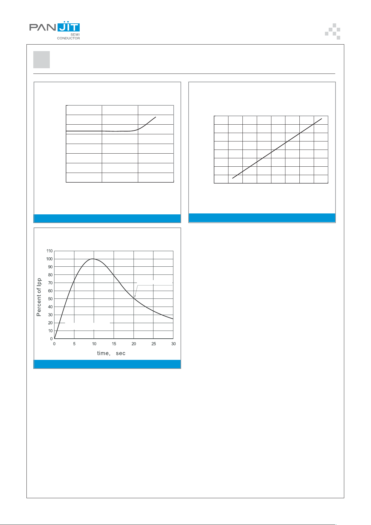
.1Fig TYPICAL CAPACITANCE
Fig PULSE WAVE FORM.2
Fig PULSE WAVE FORM.3
0.80
0.70
0.60
J
0.50
0.40
0.30
0.20
0.10
Capacitance C pF,,
0.00
0246
16
14
12
10
8
6
4
2
Peak Pulse Current Ipp A,
0
6 8 10 12 14 16 18 20 22
Reverse Bias Voltage V V,
.1Fig TYPICAL CAPACITANCE
Rise time 10-90% - 8 sm
Fig PULSE WAVE FORM.3
R
50% of Ipp @20 sm
Clamping Voltage V V,
Fig PULSE WAVE FORM.2
C
PAGE . 2September 4,2013-REV.06
 Loading...