

Page 1
Global LCD Panel Exchange Center
㪫㪜㪥㪫㪘㪫㪠㪭㪜
No. Item Page
COVER
-
-
RECORD OF REVISION
DESCRIPTION
-
ABSOLUTE MAXIMUM RATINGS
1
INITIAL OPTICAL CHARACTERISTICS
2
ELECTRICAL CHARACTERISTICS
3
BLOCK DIAGRAM
4
INTERFACE PIN ASSIGNMENT
5
INTERFACE TIMING
6
DESIGNATION OF LABEL
7
COSMETIC SPECIFICATIONS
8
PRECAUTION
9
DIMENSIONAL OUTLINE
10
www.panelook.com
Date:July.28, 2011
ATD-4950
TECHNICAL DATA
VVF42F118G00
CONTENTS
1-1/1
2-1/1
3-1/1
4-1/1
5-1/2~2/2
6-1/1
7-1/1
8-1/6~6/6
9-1/3~3/3
10-1/1
11-1/2-2/2
12-1/5~5/5
13-1/3~3/3
Panasonic Liquid Crystal Display Co.,Ltd.
Date July.28.2011 Sheet No.
㪭㪭㪝㪋㪉㪝㪈㪈㪏㪞㪇㪇㪄㪈
One step solution for LCD / PDP / OLED panel application: Datasheet, inventory and accessory!
Page
1-1/1IPS4PS 2601
www.panelook.com
Page 2

Global LCD Panel Exchange Center
The upper section : Previous revision
The lower section : New revision
Sheet No. Page
www.panelook.com
RECORD OF REVISION
SummaryDate
Panasonic Liquid Crystal Display, Ltd.
Date July.28,2011 Sheet No.
IPS4PS 2-1/1PageVVF42F118G00-12602
One step solution for LCD / PDP / OLED panel application: Datasheet, inventory and accessory!
www.panelook.com
Page 3

Global LCD Panel Exchange Center
The following specifications are applied to the following IPS-Pro-TFT LCD module.
www.panelook.com
DESCRIPTION
Product Name :
Effective display area : (H) 930.24 × (V) 523.26 (mm)
Number of pixels : (H) 1,920 × (V) 1,080 (pixels)
Pixel pitch : (H) 0.4845 × (V) 0.4845 (mm)
Color pixel arrangement : R+G+B vertical stripe
Display mode : Transmissive mode
Normally black mode
Top polarizer type : Semi-Glare
VVF42F118G00
General Specifications
Number of colors : 1,073,741,824 (colors)
External dimensions : Typ. (H) 966.64 × (V) 562.76 × (T) (3) (mm)
Weight : Typ. 2,200 (g)
Panasonic Liquid Crystal Display, Ltd.
Date July.28,2011 Sheet No. IPS4PS 3-1/1PageVVF42F118G00-12603
One step solution for LCD / PDP / OLED panel application: Datasheet, inventory and accessory!
www.panelook.com
Page 4

Global LCD Panel Exchange Center
n
1. ABSOLUTE MAXIMUM RATINGS
1. 1 Environmental Absolute Maximum Ratings
ITEM
Temperature 0 40 -20
Humidity 2)
Vibration -
Shock
Corrosive Gas
Illumination at
LCD Surface
Note 1) Temperature and Humidity should be applied to the glass surface of a IPS-Pro TFT LCD module, not to
the system installed with a module.
2) Ta҇40 Relative humidity should be less than 85 %RH max. Dew is prohibited.
Ta㧪40 Relative humidity should be lower than the moisture of the 85 %RH at 40 .
3) Frequency of the vibration is between 15 Hz and 100 Hz. (Remove the resonance point) 1 hour.
4) Pulse width of the shock is 10 ms.
5) Long operation under low temperature may cause some portion of display area to be reddish for
several minutes after turning on the product.
However, it does not affect the characteristics and reliability of the product.
6) Environmental Absolute Maximum Ratings is Based on IPS Alpha Technology TFT standard module.
Leave TFT open cell alone,this environmental ratings can't be guaranteed.The users have a responsibility
in considering ability of other parts of TFT module and TFT module process.
Min. Max.
-
Not Acceptable
- 50,000 - 50,000 1x
Operating
www.panelook.com
4.9(0.5 G)
29.4(3 G)
Storage
Min. Max.
60
2) 㧑RH
-
-
196(20G)
Not Acceptable -
UNIT
m/s
m/s
NOTE
1),5),6)
1)
2
2
3)9.8(1.0G)
4),5)
1. 2 Electrical Absolute Maximum Ratings
(1)TFT-LCD module GND = 0 V
ITEM SYMBOL
Min. Max.
UNIT NOTE
Source Driver Analog Power Supply AVDD -0.3 18 V
Source Driver Analog Power Supply-1 AVDDMH -0.3 AVDD
Source Driver Analog Power Supply-2 AVDDML -0.3
AVDD V
Driver Logic Power Supply VDD -0.3 4.0
Gate Driver Power Supply VON
-0.3
VOFF+44
Gate Driver Ground VOFF -22 0.3
V
V
V
V
Gate Driver Power Supply Range VON-VOFF -0.3 45 V
VREF1䌾5 AVDD-10.5 AVDD+0.3 V
Gamma Corrected Power Supply
VREF6 AVDD-10.5 10.5 V
VREF8䌾12 -0.3 10.5 V
Input Voltage for logic V
Electrostatic Durability V
1 -0.3
ESD0
VDD + 0.3 V 1)
㫧㪈㪇㪇
V 2),3)
Note 1) It is applied to pixel data sig
2) Discharge Coefficient : 200 pF - 250 , Environmental : 25 㷄 - 70䋦RH
3) It is applied to I/F connector pins.
1.3 Environmental Absolute Ratings of TFT open cell
Storage Condition : With shipping package
Storage temperatue range : 25±5䇭㷄
Storage humidity range : 50±10%RH
Shelf life : a month
Panasonic Liquid Crystal Display, Ltd.
One step solution for LCD / PDP / OLED panel application: Datasheet, inventory and accessory!
Date
July.28,2011 Sheet No.
IPS4PS 4-1/1PageVVF42F118G00-12604
www.panelook.com
Page 5

Global LCD Panel Exchange Center
X
2. INITIAL OPTICAL CHARACTERISTICS
The following optical characteristics are measured under stable conditions. It takes about 30 minutes to reach stable
conditions. The measuring point is the center of display area unless otherwise noted.
The optical characteristics should be measured in a dark room or equivalent state.
Measuring equipment : CS-1000A, or equivalent
Ambient Temperature =25 , V
Ifc = 68mA/string ( On-duty=100% )
Light source is backlight of Panasonic Liquid Crystal Display Co.,Ltd. TFT standard module.
%4
Response
time
Rise t
Fall t
Brightness of white B
Brightness uniformity B
Red
Color
Green
chromaticity
㧔CIE㧕
Blue
White
Red
Variation of
Green
color position
(CIE)
Blue
White
on -
off
wh 350 450 -
uni --
x 0.560 0.590 0.620
[
x 0.310 0.340
[
x 0.125 0.155 0.185
[
x 0.250 0.280
[
x
y
x
y
x
y - - 0.04
x - -
y - - 0.04
www.panelook.com
DD=12.0 V , f V=120 Hz ,
800
㧩 0 °
1)
㧩 50 °
㧩 0 °,
ޓޓ 90 °,
ޓޓ180 °,
ޓޓ270 °
1)
0.305 0.335 0.365
0.570 0.600 0.630
0.035 0.065 0.095
0.253 0.283 0.313
Typ. Max. UNIT NOTEITEM SYMBOL CONDITION Min.
1400 - - 2)Contrast ratio
10 20 ms 3)
- 8 16 ms
cd/m
40
㧑
0.370
0.310
- - 0.04
- - 0.04
- - 0.04
- - 0.04 -
- - 0.04
0.04
3)
2
4)
-
ޣGray scale
=1023ޤ
5)
䇼Gray scale
=1023䇽
Note 1) Definition of viewing angle
=90°
(12 o'clock)
=180°
(9 o'clock)
X'
TFT - LCD module
- - - Estimated valueContrast ratio at 89 ° CR89 6) 10
=0°
Y
Z
eye
=0°
(3 o'clock)
Z'
Y'
=270°
(6 o'clock)
Panasonic Liquid Crystal Display, Ltd.
One step solution for LCD / PDP / OLED panel application: Datasheet, inventory and accessory!
Date July.28,2011 Sheet No. IPS4PS 5-1/2PageVVF42F118G00-12605
www.panelook.com
Page 6

Global LCD Panel Exchange Center
f
Note 2) Definition of contrast ratio (CR)
(Luminance at displaying WHITE)
CR=
(Luminance at displaying BLACK)
3) Definition of response time
Displaying
data signal
%
100
Optical
response
(Luminance)
4) Definition of brightness uniformity
Display pattern is white (1023 level) . The brightness uniformity is defined as the following equation.
Brightness at each point is measured, and average, maximum and minimum brightness is calculated.
uni=
B
where, B
B
B
90
10
max = Maximum brightness
min = Minimum brightness
ave = Average brightness
B
www.panelook.com
BLACK WHITE
ton tof
0
max or Bmin - Bave
B
Bave
9
(B(k))
ave=
k=1
䋹
×100
BLACK
10%
50%
90%
10% 50% 90%
: measuring points
5) Variation of color position on CIE
Variation of color position on CIE is defined as difference between colors at = 0° and at = 50°& = 0°,
90°, 180°, 270°.
6) Contrast ratio at 89 °
Evaluetion conditions are on horizontal & vertical axis
Panasonic Liquid Crystal Display, Ltd.
One step solution for LCD / PDP / OLED panel application: Datasheet, inventory and accessory!
Date July.28,2011 Sheet No.
IPS4PS 5-2/2PageVVF42F118G00-12605
www.panelook.com
Page 7
Global LCD Panel Exchange Center
H
L
0
3. ELECTRICAL CHARACTERISTICS
3. 1 TFT-LCD module Ta = 25 , GND = 0 V
ITEM SYMBOL Min. Typ.
Source Driver Analog
Power Supply Voltage
Ripple voltage of AVDD Vrip_avdd - - 300 mV 1), 3)
Source Driver Analog
Power Supply Voltage-1
Ripple voltage of AVDDMH
Source Driver Analog
Power Supply Voltage-2
Ripple voltage of AVDDML
Driver Logic Power Supply Voltage VDD 2.4 2.5 2.6 V
Ripple voltage of VDD Vrip_vdd - - 150 mV 1), 3)
Gate Driver Power Supply Voltage VON 29.0 30.5 32.5 V
Ripple voltage of VON Vrip_von - - 500 mV 1), 3)
Gate Driver Ground Voltage VOFF -6.35 -5.8 -5.25 V
Ripple voltage of VOFF Vrip_voff - - 200 mV 1), 3)
Input High Voltage for logic VIH1 0.8VDD - VDD V 2)
Input Low Voltage for logic VIL1 0 - 0.2VDD V 2)
Common Plate Voltage VCOM - 4.548 - V
Ripple voltage of VCOM Vrip_vcom - - 200 mV 1), 3)
Source Driver Analog Power Supply Current
Source Driver Analog Power Supply-1 Current
Source Driver Analog Power Supply-2 Current
Driver Logic Power Supply Current IDD - 60 100 mA 1)
Gate Driver Power Supply Current ION - 6.0 10 mA 1)
Gate Driver Ground Current IOFF -10.0 -6.0 - mA 1)
Gamma Corrected Power Supply Voltage 1 VREF1 - 12.193 - V
Gamma Corrected Power Supply Voltage 2 VREF2 - 10.718 - V
Gamma Corrected Power Supply Voltage 3 VREF3 - 9.353 - V
Gamma Corrected Power Supply Voltage 4 VREF4 - 8.690 - V
Gamma Corrected Power Supply Voltage 5 VREF5 - 8.186 - V
Gamma Corrected Power Supply Voltage 6 VREF6 - 6.354 - V
Gamma Corrected Power Supply Voltage 8 VREF8 - 4.426 - V
Gamma Corrected Power Supply Voltage 9 VREF9 - 3.945 - V
Gamma Corrected Power Supply Voltage 1
Gamma Corrected Power Supply Voltage 11 VREF11 - 1.893 - V
Gamma Corrected Power Supply Voltage 12 VREF12 - 0.393 - V
Note 1)
fV=120.0Hz䋬fCLK=240.0MHz䋬each power supply voltage is typical condition and display pattern is white raster
DC ampere meter
www.panelook.com
Max. UNIT NOTE
AVDD 12.286 12.586 12.886 V
AVDDMH VREF6+0.2 6.70 6.85 V
rip_avddm
AVDDML 5.85 6.00 VREF6-0.2 V
rip_avddm
IADD - 200 300 mA 1)
IADDH - 175 250 mA 1)
IADDL -250 -175 - mA 1)
VREF10 - 3.269 - V
- - 300 mV 1), 3)
- - 300 mV 1), 3)
200 mV 3), 4)Ripple voltage of VREF Vrip_VREF - -
AVDD, VDD, VON, VOFF
TFT module
GND
2) It is applied to LP, POLR, POLL, CPV, DATA1 and DATA2 signal.
3) The above specification is defined at connector CN1 and CN2.
4) Display pattern is 128gray raster.
Panasonic Liquid Crystal Display, Ltd.
One step solution for LCD / PDP / OLED panel application: Datasheet, inventory and accessory!
Date July.28,2011 Sheet No.
6-1/1PageVVF42F118G00-12606IPS4PS
www.panelook.com
Page 8
Global LCD Panel Exchange Center
D288
D288
D576
D1
D2
D288
S
i
i
i
g
ig
l
g
S
i
i
i
g
ig
l
pp
y
G
i
i
i
g
ig
l
pp
y
g
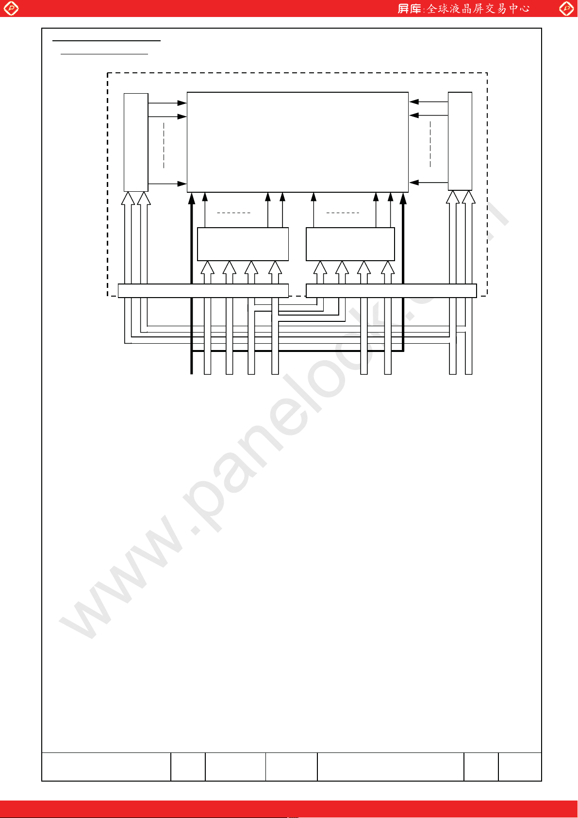
4. BLOCK DIAGRAM
4. 1 TFT-LCD module
www.panelook.com
G1
G2
Gate Driver
G1080
G1
G2
TFT-LCD
Gate Driver
G1080
Source Driver Source Driver
CN2 CN1
e
VCOM volta
mini-LVDS Display data
e
na
s
n
m
ver T
Gamma reference volta
ource Dr
l
DC Power su
na
s
n
m
ver T
mini-LVDS Display data
ource Dr
l
na
s
n
m
DC Power su
ver T
ate Dr
One step solution for LCD / PDP / OLED panel application: Datasheet, inventory and accessory!
Panasonic Liquid Crystal Display, Ltd.
Date July.28,2011 Sheet No. IPS4PS 7-1/1PageVVF42F118G00-12607
www.panelook.com
Page 9
Global LCD Panel Exchange Center
㪚㪥㪉
㪚㪥㪈
5. INTERFACE PIN ASSIGNMENT
5. 1 TFT-LCD module
CN1:MOLEX 503366-6011
PIN
SYMBOL DESCRIPTION NOTE
No.
1 VCOM-SL Common Voltage 31 GND GND(0V)
2 LPL
4 N.C. Non Conection
5 VGMA12
VGMA11
6
7 VGMA10
8 VGMA9
9 VGMA8
10 N.C.
11
12 AVDD
14 AVDDMH
15 AVDDMH
16 AVDDML
17 AVDDML
18
19 LV7BL
20 LV7AL
21 LV6BL
22
23 GND
24 LV5BL
25 LV5AL
26
27
28 GND
29 CLKBL
30 CLKAL 60 VCOM
GND
LV6AL 52 VGMA2
LV4BL
LV4AL
Control Signal
Reference Voltage
Non Conection
GND(0V)GND
Analog Voltage
Analog Voltage
Analog Voltage
GND(0V)
Pixel Data
Pixel Data
GND(0V)
Pixel Data
Pixel Data
GND(0V) 58 GND GND(0V)
Pixel Clock
www.panelook.com
PIN
SYMBOL DESCRIPTION NOTE
No.
32 LV3BL
33 LV3AL3 POLL Control Signal
34 LV2BL
35 LV2AL
36 GND
37 LV1BL
38 LV1AL
39 LV0BL
40
LV0AL
41 GND GND(0V)
42 VOFF
43 VONL13 AVDD
DATA2L
DATA1L
45
46
47 N.C.
48 VGMA6
49 VGMA5
50 VGMA4
51 VGMA3
53 VGMA1
54 GND
55 GND
56 VDD
57 VDD
59 VCOM
CPVL
Pixel Data
Pixel Data
GND(0V)
Pixel Data
Pixel Data
Reference Voltage
Control Signal44
Control Signal
Control Signal
Non Conection
Reference Voltage
GND(0V)
Logic Voltage
Common Voltage
㪩㪼㪸㫉㩷㫍㫀㪼㫎㩷㫆㪽㩷㪣㪚㪤
Panasonic Liquid Crystal Display, Ltd.
䂥
㪥㫆㪅㪍㪇
Date July.28,2011 Sheet No. IPS4PS 8-1/4PageVVF42F118G00-12608
㩷㩷㩷䂥
㪥㫆㪅㪈
One step solution for LCD / PDP / OLED panel application: Datasheet, inventory and accessory!
䂥
㪥㫆㪅㪍㪇
䂥
㪥㫆㪅㪈
www.panelook.com
Page 10

Global LCD Panel Exchange Center
㪚㪥㪉
㪚㪥㪈
5. INTERFACE PIN ASSIGNMENT
5. 1 TFT-LCD module
CN2:MOLEX 503366-6011
PIN
SYMBOL DESCRIPTION NOTE
No.
1 N.C. Non Conection 31 GND GND(0V)
2 LPR Control Signal 32 LV3BR
4 N.C. Non Conection 34 LV2BR
6 VGMA11
7 VGMA10
8 VGMA9
9 VGMA8
10 N.C. Non Conection 40 LV0AR
11 GND GND(0V) 41 GND GND(0V)
12 AVDD
13 AVDD
14 AVDDMH
15 AVDDMH
16 AVDDML
17 AVDDML
18 GND GND(0V) 48 VGMA6
19 LV7BR
20 LV7AR
21 LV6BR
22 LV6AR 52 VGMA2
23 GND GND(0V) 53 VGMA1
24 LV5BR
25 LV5AR
26 LV4BR
27 LV4AR
28 GND GND(0V) 58 GND GND(0V)
29 CLKBR
30 CLKAR
Reference Voltage
Analog Voltage
Analog Voltage
Analog Voltage
Pixel Data
Pixel Data
Pixel Data
Pixel Data
Pixel Clock
www.panelook.com
PIN
SYMBOL
No.
33POLR Control Signal
LV3AR3
35 LV2AR5 VGMA12
36 GND GND(0V)
37 LV1BR
38 LV1AR
39 LV0BR
42 VOFF
43 VONR
44 DATA2R Control Signal
45 DATA1R Control Signal
46 CPVR Control Signal
47 N.C. Non Conection
49 VGMA5
50 VGMA4
51 VGMA3
54 GND
55 GND
56 VDD
57 VDD
59 VCOM
60 VCOM
DESCRIPTION NOTE
Pixel Data
Pixel Data
Pixel Data
Pixel Data
Reference Voltage
Reference Voltage
GND(0V)
Logic Voltage
Common Voltage
㪩㪼㪸㫉㩷㫍㫀㪼㫎㩷㫆㪽㩷㪣㪚㪤
Panasonic Liquid Crystal Display, Ltd.
䂥
㪥㫆㪅㪍㪇
Date July.28,2011 Sheet No. 8-2/4PageVVF42F118G00-12608IPS4PS
㩷㩷㩷䂥
㪥㫆㪅㪈
One step solution for LCD / PDP / OLED panel application: Datasheet, inventory and accessory!
䂥
㪥㫆㪅㪍㪇
䂥
㪥㫆㪅㪈
www.panelook.com
Page 11

Global LCD Panel Exchange Center
-
-
-
-
-
-
-
-
R
R
R
R
R
R
R
R
R
5. 3 Correspondence between input data and display image
Display data of adjacent two pixel is latched during fore cycle of CLK.
B G R G0 - G7 : G (x,y)
(1,1) (1,1) (1,1) B0 - B7 : B (x,y)
1 , 1 1 , 2 1 , 3 1 , 959 1 , 960 1 , 961 1 , 962 1 , 1919 1 , 1920
2 , 1 2 , 2 2 , 3 2 , 959 2 , 960 2 , 962 2 , 962 2 , 1919 2 , 1920
3 , 1 3 , 2 3 , 3 3 , 959
- - - - - - - - - - -
- - - - - - - - - - -
- - - - - - - - - - -
www.panelook.com
Pixel : R0 - R7 : R (x,y)
upper
3 , 960 3 , 963 3 , 962 3 , 1919 3 , 1920
- - - - - - - - - - -
- - - - - - - - - - -
- - - - - - - - - - -
1080 , 1 1080 , 2 1080 , 3
- - - - - - - - - - -
case:PCB in the panel upper part & Zigzag panel
CLK*R/CLK*
LV0*
LV1*
LV2*
Invalid
Invalid
R(1,1920)
R(1,1918) R(1,964)
G(1,1920)
G(1,1918) G(1,964)
B(1,1919) B(1,965) B(1,963)
LV3*
LV4*
LV5*
LV6*
B(1,1918)
R(1,1919) R(1,1917) R(1,963)
Invalid
G(1,1919)
G(1,1917)
B(1,964)
G(1,963) G(1,961)
B(1,1920)
LV7*
LV0*L
LV1*L
LV2*L
LV3*L
LV4*L
LV5*L
LV6*L
LV7*
B(1,961)
R(1,960) R(1,958) R(1,4)
G(1,960) G(1,958) G(1,4)
B(1,960) B(1,958)
R(1,959) R(1,957)
Invalid
G(1,959) G(1,957)
B(1,959)
B(1,5)
B(1,4)
R(1,3)
G(1,3)
LP
1080 , 959 1080 , 960 1080 , 961 1080 , 962 1080 , 1919
- - - - - - - - - - -
lower
R(1,962)
G(1,962)
B(1,962)
R(1,961)
B(1,3)
R(1,2)
G(1,2)
B(1,2)
R(1,1)
G(1,1)
Invalid
Invalid
B(1,1)
Invalid
Invalid
Invalid
Invalid
Invalid
InvalidInvalid
Invalid
R(1,1920)
G(1,1920)
B(1,1920)
R(1,1919)
G(1,1919) G(1,1917)
B(1,1919)
R(1,960)
G(1,960) G(1,958)
B(2.960)
R(1,959) R(1,957)
G(1,959) G(1,957)
B(1,959) B(1,957)
R(1,1918)
G(1,1918)
B(1,1918)
R(1,1917)
B(1,1917)
R(1,958)
B(1,958)
R(2.964)
R(2,962)
G(2.964)
G(2,962)
B(2,962)
B(1,954)
R(2.963)
R(2,961)
G(2.963)
G(2,961)
B(2.963)
B(2,961)
R(2.4) R(2,2)
G(2.4) G(2,2)
B(2.4)
R(2.3)
G(2.3)
B(2.3)
B(2.2)
R(2,1)
G(2,1)
B(2,1)
1080 , 1920
Invalid
Invalid
Invalid
Invalid
data mapping
Odd line Even line
CLK*R/CLK*
LV0*R/LV4*R
/LV0*L/LV4*L
B2 B3 B4 B5 B6 B7
LV1*R/LV5*R
/LV1*L/LV5*L
LV2*R/LV6*R
/LV2*L/LV6*L
R2 R3 R4 R5 R6 R7
G2 G3 G4 G5 G6 G7
LV3*R/LV7*R
/LV3*L/LV7*L
Panasonic Liquid Crystal Display, Ltd.
One step solution for LCD / PDP / OLED panel application: Datasheet, inventory and accessory!
Date July.28,2011 Sheet No.
Pixel:
R0 R1 G0 G1B0 B1
B(x,y-1)
R(x,y)
G(x,y)
CLK*R/CLK*
LV0*R/LV4*R
/LV0*L/LV4*L
LV1*R/LV5*R
/LV1*L/LV5*L
LV2*R/LV6*R
/LV2*L/LV6*L
LV3*R/LV7*R
/LV3*L/LV7*L
IPS4PS 8-3/4PageVVF42F118G00-12608
G(x,y)
Pixel:
R2 R3 R4 R5 R6 R7
G2 G3 G4 G5 G6 G7
B2 B3 B4 B5 B6 B7
R0 R1 G0 G1 B0 B1
R(x,y)
B(x,y)
www.panelook.com
Page 12

Global LCD Panel Exchange Center
)
)
)
5. 4 Relationship between display colors and input signals
Input
R7 R6 R5 R4 R3 R2 R1 R0 G7 B7 B6 B5 B4 B3 B2 B1 B0
Color
Black 000000000000000000000000
Red(255) 111111110000000000000000
Green(255
Basic Blue(255) 0000000 000000011111111
Color Cyan 000000001111111111111111
Magenta 111111110000000011111111
Yellow 1111111 111111100000000
White 111111111111111111111111
Black 0000000 000000000000000
Red (1) 000000 00000000000000
Red (2) 0000001 00000000000000
Red : :::::: ::::::::::::::::
Red(254) 111111 01 00000000000
Red(255) 11111111 000000000000000
Black 000000000000000000000000
Green (1) 000000000000000100000000
Green (2) 000000000000001000000000
Green : : : ::::::::::::::::::::
Green(254
Green(255
Black 000000000000000000000000
Blue (1) 000000000000000000000001
Blue (2) 00000000 00000 00000000010
Blue : ::::::::::::::::::::::::
Blue (254) 00000000 000000 0011111110
Blue (255) 00000000000 1111111100000
MSB LSB MSB LSB MSB LSB
000000001111111100000000
: :::::::: :::::: ::::::::
: ::::::::::::::::::::::::
000000001111111000000000
000
: ::::::::::::::::::::::::
Red Data Green Data
::
000001111111100000000
www.panelook.com
G6 G5 G4 G3 G2 G1 G0
00
11
00
0
1
000
::
0
0
00
0
000
Blue Data
::
Note 1) Definition of gray scale :
Color(n)
Larger n correspondsto brighter level.
2) Data : 1 : High, 0 : Low
Panasonic Liquid Crystal Display, Ltd.
One step solution for LCD / PDP / OLED panel application: Datasheet, inventory and accessory!
Number in parenthesis indicates gray scale level.
Date July.28,2011 Sheet No.
IPS4PS 8-4/4PageVVF42F118G00-12608
www.panelook.com
Page 13

Global LCD Panel Exchange Center
K
K
(VI)
6. INTERFACE TIMING
6. 1 mini-LVDS receiver timing
www.panelook.com
CLK+/-
LV0+/-
to
LV5+/-
PWCLK
PWCLK(H) PWCLK(L)
tR
+150mV
tF
tF
-150mV
tR
+150mV
tHOLD1
tSETUP1 tHOLD1 tSETUP1
CLK
LV0
to
LV5
-150mV
LVn=(LVn+)-(LVn-)䇭n=0䌾5
CLK=(CLK+)-(CLK-)
ITEM SYMBOL Min. Typ. Max. UNIT NOTE
Clock period PWCLK 4 4.17 4.3 ns 1)
Clock high level width PWCLK(H) 1.7 2.085 - PWCL
Clock Low level width PWCLK(L) 1.7 2.085 - PWCL
Data setup time tSETUP1 0.65 1.04 - ns 1)
Data hold time tHOLD1 0.65 1.04 - ns 1)
mini-LVDS rise time tR - - 0.5 ns 1)
mini-LVDS fall time tF - - 0.5 ns 1)
mini-LVDS differential voltage
mini-LVDS common mode
input voltage range
VID 150 412 600 mV 1)
VI 0.5 0.8 1.1 V 1)
+VID
-VID
+VID
-VID
Center
(VI)
Center
GND
GND
1)
1)
Notes 1) The above specification is defined at each Source Driver IC inputs.
Panasonic Liquid Crystal Display, Ltd.
Date July.28,2011 9-1/4PageVVF42F118G00-12609
Sheet No. IPS4PS
One step solution for LCD / PDP / OLED panel application: Datasheet, inventory and accessory!
www.panelook.com
Page 14

Global LCD Panel Exchange Center
6. 2 Control signal timing
Notes 1) The following specification is defined at connector CN1.
www.panelook.com
tPWLP
LP
POLL, POLR
0.8VDD
0.2VDD
tPOL-LP tLP-POL
0.8VDD
0.2VDD
0.8VDD
0.2VDD
0.8VDD
0.2VDD
ITEM SYMBOL Min. Typ. Max. UNIT NOTE
Latch clock high level width tPWLP 0.2 0.58 - s
POL setup time tPOL-LP 1.0 2.17 - s
POL hold time tLP-POL 1.0 5.41 - s
tPWCPVL tPWCPVH tCPV
CPV
0.8VDD
0.2VDD 0.2VDD 0.2VDD
tSETUP2 tHOLD2 tSETUP2
0.8VDD
tHOLD2
DATA1, DATA2
0.8VDD 0.8VDD
Typ. Max. UNIT NOTEITEM SYMBOL Min.
Gate shift clock period
tCPV
7.46 7.58 7.88
Gate shift clock high level width tPWCPVH 0.7 0.88 1.0 s
- 6.6Gate shift clock low level width tPWCPVL
-s
Data setup time tSETUP2 0.3 0.44 - s
Data hold time tHOLD2
䌴CPV-LP
0.8VDD
0.3 0.44
䌴LP-CPV
-s
䌴CPV-LP
0.8VDD
LP
0.8VDD
0.8VDD
CPV
s
ITEM SYMBOL Min. Typ. Max. UNIT NOTE
Gate delay time tCPV-LP 0.97
TFT charge time tLP-CPV - 6.51
Panasonic Liquid Crystal Display, Ltd.
Date July.28,2011
1.07
Sheet No. IPS4PS 9-2/4PageVVF42F118G00-12609
1.17 s
-s
One step solution for LCD / PDP / OLED panel application: Datasheet, inventory and accessory!
www.panelook.com
Page 15

Global LCD Panel Exchange Center
K
N/AN/AN/AN/AN/AN/AN/AN/AN/AN/AN/AN/AN/AN/AN/AN
0.8VDD
LP
CLK
0.2VDD
www.panelook.com
tLP-RST
Reset command
LV0
"H" "H" "H" "H" "H" "L" "L" "L"
LV1
/A
to
ITEM SYMBOL Min. Typ.
Reset input time tLP-RST 24 -
Valid DATA
Valid DATA
Max. UNIT NOTE
- PWCL
Panasonic Liquid Crystal Display, Ltd.
One step solution for LCD / PDP / OLED panel application: Datasheet, inventory and accessory!
Date July.28,2011 Sheet No. IPS4PS 9-3/4PageVVF42F118G00-12609
www.panelook.com
Page 16

Global LCD Panel Exchange Center
6.4 Timing between interface signals power supply
Notes 1) The following specification is defined at connector CN1and CN2.
2) In the T10 and T11, the float equal to or less than 1.5V of AVDD is no object.
3) In the T20 and T21, the float equal to or less than 1.5V of VON is no object.
4) In a period of T1, must set SDA='H' and SCL='H' or 'L'.
Power Supply
DD
V
2.5V
0V
2.2V
0.2V
T1
www.panelook.com
T2 T3
T5
T7
2.2V
T15
T4
0.2V
Logic Signals
ON
Backlight
ON/OFF
Source Driver & VCOM Sequence
0V
2.2V
OFF
0䇭㻡䇭T1䇭㻡䇭10
350䇭㻡䇭T2
T10
T11
0.3V
T13
T12
T14
VRF1~VRF12
Logic Signals
0䇭䇭 㻡䇭T3
20 㻡䇭T4
0䇭 㻡䇭T5
0 㻡䇭T6
䌔7 don't care
AVDD
VCOM
AVDDMH
AVDDML
VDD
Logic Signals
T15
T16
T17
T19
T6
0䇭㻡䇭䌔10
䇭䇭䇭䇭 T11 㻡䇭10
0䇭㻡䇭T12, T13, T14
0䇭㻡䇭T15, T16, T17
T18 㻡䇭1000
0䇭㻡䇭T19
T18
0.8V
Gate Driver Sequence
VON
T20
2.2V
0V
Panasonic Liquid Crystal Display, Ltd.
T22
VDD
Logic Signals
-0.3V -0.8V
T21
Date July.28,2011 Sheet No. IPS4PS
VOFF
T23
0䇭㻡䇭T20
䇭䇭䇭 T21䇭㻡 10
0 㻡 T22
T23䇭㻡 1000
0.8V0.3V
One step solution for LCD / PDP / OLED panel application: Datasheet, inventory and accessory!
Unit : ms
9-4/4PageVVF42F118G00-12609
www.panelook.com
Page 17

Global LCD Panel Exchange Center
f
7. DESIGNATION OF LABEL
7.1 Label
The barcode label is pasted on each TFT open cell.
Users use this bar code label to write adjustment Vcom value and Liquid Crystal information to Tcon ROM which is speci
by Panasonic Liquid Crystal Display Co.,Ltd.
www.panelook.com
㽲
㪭㪭㪝㪋㪉㪝㪈㪈㪏㪞㪇㪇
㪪㪘㪤㪧㪣㪜㪇㪇㪇㪈 㪘
㪁
Item Description
㽲
㽳
㽴
㽵
㽶
㽷
Product Name
Rev. is the column for manifacturing convinience. A-Z except I and O may be written on this column.
Lot mark
Liquid crystal information
Marker A : A, C, E, G, J, L, N, R
Marker B : B, D, F, H, K, M, P, S
Bar code(㽴+㽵)
Bar code(IPS inner management barcode)
㽴
㽳
㪩㪼㫍
㽷
㽶
㪁
㽵
7.2 Record of revision described on the label
Rev.BG = B grade cosmetic specifications
Panasonic Liquid Crystal Display, Ltd.
Date July.28,2011 Sheet No.
One step solution for LCD / PDP / OLED panel application: Datasheet, inventory and accessory!
10-1/1IPS4PS 2610 VVF42F118G00-1 Page
www.panelook.com
Page 18

Global LCD Panel Exchange Center
f
8. COSMETIC SPECIFICATIONS
8.1 Condition for cosmetic inspection
(1) Viewing zone
a) The figure shows the correspondence between
eyes (of inspector) and TFT-LCD module.
㻡45䉙: when non-operating inspection
㻡5䉙 : when operating inspection
I
www.panelook.com
Inspection view
Light
b) Inspection should be executed only from
front side and only A-zone.
Cosmetic of B-zone and C-zone are ignore.
(refer to 9.2 Definition of zone)
(2) Environmental
a) Temperature : 25 degrees
b) Ambient light : about 700 lx and non-directive when operating inspection.
: about 1000 lx and non-directive when non-operating inspection.
c) Backlight : when non-operating inspection, backlight should be off .
8.2 Definition of zone
䍃A-zone : Display area (pixel area)
䍃B-zone : Area between A-zone and C-zone
䍃C-zone : Metallic bezel area
about 500mm
TFT-LCD module
㪘㪄㫑㫆㫅㪼
㪙㪄㫑㫆㫅㪼
㪚㪄㫑㫆㫅㪼
8.3 Cosmetic specifications
When displaying conditions are not stable (ex. at turn on or off), the following specifications are not applied.
Max. acceptable number
A-zone
Unit NoteNo ITEM
Bgrade
1-dot pcs6
Operating
inspection
Sparkle
mode
1 Dot defect
Black
mode
2 Line defect
3 Uneven brightness
2-dots 2
3-dots 1
Density
Total 7 pcs 1),2)
1-dot
2-dots 3
3-dots 1
Density
Total 15 pcs 1),3)
Total 21
3
15 pcs 1),3),4)
4 pcs/20mm 1),3),6)
Serious one is
not allowed
Units 1),2),5)
pcs/20mm 1),2),6)
Units
pcs
--
1),2),4)
1),3),
5),10)
1)
Panasonic Liquid Crystal Display, Ltd.
One step solution for LCD / PDP / OLED panel application: Datasheet, inventory and accessory!
Date July.28,2011 Sheet No.
11-1/2IPS4PS 2611 VVF42F118G00-1 Page
www.panelook.com
Page 19

Global LCD Panel Exchange Center
Stain inclusion
4
5
Operating
inspection
6
7
Non
operating
inspection
9 Wrinkles on polarizer
Line shape
W : width (mm)
L : length (mm)
Stain inclusion
Dot shape
D : ave. dia (mm)
Scratch on polarizer
Line shape
W : width (mm)
L : length (mm)
Scratch on polarizer
Dot shape
D : ave. dia (mm)
Bubbles, peeling
in polarizer
D : ave. dia (mm)
www.panelook.com
Max. acceptable number
A-zone
Bgrade
W㻡0.08
W㻡0.25
W>0.25
W㻡0.15 L : Ignore Ignore
W>0.3 - 0
L : Ignore Ignore
L㻡㪉.0 16
2.0䋼L㻡4.0 8
L>4.0 0
- (See dot shape)
D㻡0.5
D>1.0 0
L㻡20 10
L>20 0
D㻡0.6 Ignore
D>1.0 0
D㻡0.5 Ignore
D>1.0 0
Ignore
Serious one is
not allowed.
Unit NoteNo ITEM
pcs 7)
pcs 7)D㻡㪈㪅㪇 8
pcs 8)W㻡0.3
pcs 8)D㻡㪈㪅㪇 10
pcs
-
8)8D㻡㪈㪅㪇 10
-
Note 1) Dot defect : defect area > 1/2 dot
2) Sparkle mode : brightness of dot is more than 30% at black. (visible to eye)
3) Black mode : brightness of dot is less than 70% at white. (visible to eye)
4) 1 dot : defect dot is isolated, not attached to other defect dot.
5) N dots : N defect dots are consecutive. (N means the number of defects dots)
6) Density : number of defect dots inside 20mm
7) Those stains which can be wiped out easily are acceptable.
8) Polarizer area inside of B-zone is not applied.
9) No major (serious) defects when viewed in gray scale mode.
Panasonic Liquid Crystal Display, Ltd.
Date July.28,2011 Sheet No. IPS4PS 2611 VVF42F118G00-1 Page 11-2/2
One step solution for LCD / PDP / OLED panel application: Datasheet, inventory and accessory!
www.panelook.com
Page 20

Global LCD Panel Exchange Center
㪚㪦㪝㩿㪞㪸㫋㪼㪀
㪚㪦㪝㩿㪛㫉㪸㫀㫅㪀
㪧㪚㪙㩿㪛㫉㪸㫀㫅㪀
㪧㪚㪙㩿㪛㫉㪸㫀㫅㪀
㪫㪝㪫㪄㪣㪚㪛㪂㪧㫆㫃㪸㫉㫀㫑㪼㫉
㪘
㪘
㪚㪦㪝㩿㪞㪸㫋㪼㪀
㪚㪦㪝㩿㪛㫉㪸㫀㫅㪀
㪧㪚㪙㩿㪛㫉㪸㫀㫅㪀
㪧㪚㪙㩿㪛㫉㪸㫀㫅㪀
㪫㪝㪫㪄㪣㪚㪛㪂㪧㫆㫃㪸㫉㫀㫑㪼㫉
㪘
㪘
㪪㪼㪺㫋㫀㫆㫅㩷㪘㪄㪘
㪫㪝㪫㪄㪣㪚㪛
㪧㫆㫃㪸㫉㫀㫑㪼㫉
㪚㫆㫅㪻㫌㪺㫋㫀㫍㪼㩷㫃㪸㫐㪼㫉
㪪㪼㪺㫋㫀㫆㫅㩷㪘㪄㪘
㪫㪝㪫㪄㪣㪚㪛
㪧㫆㫃㪸㫉㫀㫑㪼㫉
㪚㫆㫅㪻㫌㪺㫋㫀㫍㪼㩷㫃㪸㫐㪼㫉
㪘㪺㫋㫀㫍㪼㩷㪘㫉㪼㪸
㪫㪝㪫㪄㪣㪚㪛㪆㪧㫆㫃㪸㫉㫀㫑㪼㫉㪙㪼㫑㪼㫃
㪚㫌㫊㪿㫀㫆㫅㩷㪫㪸㫇㪼
䇭䌴㻢 㪇㪅㪍
㪤㫆㫃㪻㪼㪻㩷㪝㫉㪸㫄㪼
㪚㫌㫊㪿㫀㫆㫅㩷㪫㪸㫇㪼
䇭䌴㻢 㪈㪅㪌
㪚㫃㪼㪸㫉㪸㫅㪺㪼㻢
㪇㪅㪌
㪘㪺㫋㫀㫍㪼㩷㪘㫉㪼㪸
㪫㪝㪫㪄㪣㪚㪛㪆㪧㫆㫃㪸㫉㫀㫑㪼㫉㪙㪼㫑㪼㫃
㪚㫌㫊㪿㫀㫆㫅㩷㪫㪸㫇㪼
䇭䌴㻢 㪇㪅㪍
㪤㫆㫃㪻㪼㪻㩷㪝㫉㪸㫄㪼
㪚㫌㫊㪿㫀㫆㫅㩷㪫㪸㫇㪼
䇭䌴㻢 㪈㪅㪌
㪚㫃㪼㪸㫉㪸㫅㪺㪼㻢
㪇㪅㪌
㪬㫅㫀㫋㩷㪑㩷㪲㫄㫄㪴
9. PRECAUTION
Please pay attention to the followings when a TFT open cell is used,
handled and mounted.
www.panelook.com
9.1 Recommendation of GND c
(1) Please connect LCD surface (front side) to GND for prevention of static charge.
䌯䌮䌮䌥䌣䌴䌩䌯n of TFT open cell
9.2 Recommendation of structure for supporting TFT-LCD Rim
(1) When the LCD is applied by stress, it occurs abnormal image quality.
(It is confirmed visually especially in case of gray raster.)
The system shown on the drawing down below is recommended to maintain the LCD
䇭 by cutting down the LCD stress.
Panasonic Liquid Crystal Display, Ltd.
Date July.28,2011 Sheet No.
One step solution for LCD / PDP / OLED panel application: Datasheet, inventory and accessory!
12-1/5IPS4PS 2612 VVF42F118G00-1 Page
www.panelook.com
Page 21

Global LCD Panel Exchange Center
㪫㪝㪫㪄㪣㪚㪛
㪧㫆㫃㪸㫉㫀㫑㪼㫉
㪚㪦㪝
㪧㪚㪙
㬍
䂾
㪫㫆㫉㪼㫃㪸㫅㪺㪼㩷㫆㪽㩷㪛㫀㫄㪼㫅㫊㫀㫆㫅㩷㪘㪃㪙㩷㻡㩷㫧㪇㪅㪍
㪚㩷㪔㩷㪇㪅㪏㪃㩷㪛㩷㪔㩷㪇㪅㪍
㪝㩷㪔㩷㪌㪇䌾㪎㪇 㪜㩷㪔㩷㪈㪉㪇䌾㪈㪊㪇
㪙
㪚
㪛
㪜
㪝
㪘
㪣㪚㪛
㪣㪚㪛㩷㫄㫆㫃㪻㩷㪽㫉㪸㫄㪼
㪚㪦㪝㩿㪞㪸㫋㪼㪀
㪚㪦㪝㩿㪛㫉㪸㫀㫅㪀
㪬㫅㫀㫋㩷㪑㩷㪲㫄㫄㪴
㪝㪔㪌㪇䌾㪎㪇䋨㪊㪉㵱䋩
㪝㪔㪎㪇䌾㪐㪇䋨㪊㪎㵱䋩
㪜㪔㪈㪉㪇䌾㪈㪊㪇䋨㪊㪉㵱䋩
㪜㪔㪈㪋㪌䌾㪈㪌㪌䋨㪊㪎㵱䋩
(2)The dimension of mold frame and LCD is reccomended as follows.
www.panelook.com
(3)The wall of the mold frame should be laid on whole sides of the LCD as much as possible.
(4)The holding space for the LCD should be maintained by the mold frame and the bezel.
(5)Screw the mold frame to the lower frame at many places to keep flatness of LCD support area.
(6)The mold frame should be the structure that is divided into four sides to keep flatness of LCD support area.
(7)LCD support surface at lower side should smooth to cutting down the LCD stress.
(Put PET tape between LCD and support area, etc.)
(8)At the time of ground connection, take a method that does not put a load to the LCD.
(9)Use silicon rubber with hardness 20 for cushion to the mold frame side.
(10)Use foaming cushion to Bezel side.
(11)Flatness of the Bezel should be 0.5 which also should be the shape does not have partial changing points.
(12)The bezel should be the structure that is divided into four sides and screwed from the upper side.
(13)The surface of the cushion (the surface which attaches to the LCD) should be mat finishing or
should put PET tape to avoid the LCD and the cushion from sticking together.
9.3 Precaution to handling and mounting
(1)The polarizer on a TFT cell should carefully be handled due to its softness, and should not be
touched, pushed or rubbed with glass, tweezers or anything than HB pencil lead. The surface of
a polarizer should not be touched and rubbed with bare hand,greasy clothed or dusty clothes.
(2) The surface of a polarizer should be gently wiped with absorbent cotton, chamois or other soft materials slightly
contained petroleum benzene when the surface becomes dirty. Normal-hexane or Isopropyl alcohol as cleaning
chemicals is recommended in order to clean adhesives which fix front/rear polarizers on a TFT cell. Other cleaning
chemicals such as acetone, toluen and alcohol should not be used to clean adhesives because they cause chemical
damage to a polarizer.
(3)Saliva or water drops should be immediately wiped off. Otherwise, the portion of a polarizer and
electronic parts may be deformed.
(4)Applying upward bend to COF may cause a malfunction electrically and mechanically.
(5)Applying too much force and stress to PCB and COF may cause a malfunction electrically and mechanically.
Panasonic Liquid Crystal Display, Ltd.
Date July.28,2011 Sheet No.
One step solution for LCD / PDP / OLED panel application: Datasheet, inventory and accessory!
12-2/5IPS4PS 2612 VVF42F118G00-1 Page
www.panelook.com
Page 22

Global LCD Panel Exchange Center
9.4 Precaution to operation
(1) The ambient temperature near the operated cell and electronic parts should be satisfied with the
ratings. Unless it meets the specifications, sufficient cooling system should be adopted to system.
(2) The spike noise causes the mis-operation of a TFT open cell. The level of spike noise should be as follows:
-200mV<=over- and under- shoot of VDD<= +200mV
VDD including over- and under- shoot should be satisfied with the absolute maximum ratings.
(3) Optical response time, luminance and chromaticity depend on the temperature of a TFT open cell.
(4) Sudden temperature change may cause dew on and/or in the a TFT open cell. Dew males damage to a
polarizer and/or electrical contacting portion. Dew causes fading of displayed quality.
(5) Fixed patterns displayed on a TFT open cell for a long time may cause after-image. It will be recovered
soon.
(6) The TFT open cell has high frequency circuits. Sufficient suppression to electromagnetic interference should
be done by system manufacturers. Grounding and shielding methods may be effective to minimize
the interference.
(7) Noise may be heard when a back-light is operated. If necessary, sufficient suppression should be
done by system manufacturers.
(8) Inserting or pulling I/F connectors causes any trouble when power supply and signal dates are
on-state.I/F connectors should be inserted and pulled after power supply and signal dates are
turned off.
www.panelook.com
9.5 Electrostatic discharge control
(1) Since a TFT open cell consists of a TFT cell and electronic circuits with CMOS-ICs, which are
very weak to electrostatic discharge, persons who are handling a TFT open cell should be grounded
through adequate methods such as a list band. Connector pins should not be touched directly
with bare hands.
(2) Protection film for a polarizer on a TFT open cell should be slowly peeled off so that the electrostatic
charge can be minimized.
9.6 Precaution to strong light exposure
(1) The TFT open cell should not be exposed under strong light. Otherwise, characteristics of a polarizer and
color filter in a TFT open cell may be degraded.
9.7 Precaution to storage
When TFT open cells for replacement are stored for a long time, following precautions should be taken care of:
(1) TFT open cells should be stored in a dark place. It is prohibited to apply sunlight or fluorescent light
during storage. TFT open cells should be stored at 0 to 35㷄 at normal humidity (60%RH or less).
(2) The surface of polarizers should not come in contact with any other object. It is recommended that
TFT open cells should be stored in the IPS Alpha Technology's shipping box.
9.8 Reliability
Since electronic components are implemented to this LCD, if water drops are adhered, it causes trouble.
So, be careful of water drops adherence. (Especially around the driver circuit and the source PCB) If
any problems or damages caused by water drops, etc. by any chance, these are not covered under
warranty.
Panasonic Liquid Crystal Display, Ltd.
Date July.28,2011 Sheet No.
One step solution for LCD / PDP / OLED panel application: Datasheet, inventory and accessory!
12-3/5IPS4PS 2612 VVF42F118G00-1 Page
www.panelook.com
Page 23

Global LCD Panel Exchange Center
9.9 Precaution to handling protection film
(1) The protection film for polarizers should be pealed off slowly and carefully by persons who are
electrically grounded with adequate methods such as a list band. Besides, ionized air should be blown
over during peeling action. Dusts on a polarizer should be blown off by an ionized nitrogen gun and
so on.
(2) The protection film should be peeling off without rubbing it to the polarizer. Because, if the film is
rubbed together with the polarizer, since the film is attached to the polarizer with a small amount
of adhesive, the adhesive may remain on a polarizer.
(3) The TFT open cell with protection film should be stored on the conditions explained in 10.7 (1). However,
in case that the storage time is too long, adhesive may remain on a polarizer even after a protection
film is peeled off. Besides, in case that a TFT open cell is stored at higher temperature and/or higher
humidity, adhesive may remain on a polarizer. The remained adhesive may cause non-uniformity
of display image.
(4) The adhesive can be removed easily with Normal-Hexane. The remained adhesive or its vestige on
the polarizer should be wiped off with absorbent cotton or other soft materials such as chamois
slightly contained Normal-Hexane.
(5) The procedure of peeling protection film on pokarizer is recommended as follows.
(5-1)Set up LCD on the rest of the cell as the lower polarizer film comes on top gently.
(5-2)Peel off protection film from lower polarizer film with tape.
The protection film should be peeled as Drawing 1 or 2.
Side of drain COF
www.panelook.com
Side of drain COF
Side of gate COF
Side of gate COF
Drawing 1 Drawing 2
(5-3)Set up LCD on the Backlight unit as the upper polarizer film comes on top gently.
(5-4)Connect LCD surface to GND.
(5-5)Peel off protection film from upper polarizer film with tape.
The protection film should be peeled as Drawing 3 or 4.
Side of gate COF
Side of drain COF
Side of gate COF
Side of drain COF
Drawing 3 Drawing 4
9.10 Safety
(1) Since a TFT cell is made of glass, handling to the broken TFT open cell should be taken
care sufficiently in order not to be injured. Hands touched liquid crystal from a broken TFT open cell should be
washed sufficiently.
9.11 Environmental protection
(1) Flexible printed circuits and printed circuits board contain small amount of lead.
Please follow local ordinance or regulations for its disposal.
Panasonic Liquid Crystal Display, Ltd.
Date July.28,2011 Sheet No.
One step solution for LCD / PDP / OLED panel application: Datasheet, inventory and accessory!
12-4/5IPS4PS 2612 VVF42F118G00-1 Page
www.panelook.com
Page 24

Global LCD Panel Exchange Center
f
9.12 Use restrictions and limitations
(1) This product is not authorized for use in life support devices or systems, military applications or
other applications which pose a significant risk of personal injury.
(2) In no event shall IPS Alpha Technology, Ltd., be liable for any incidental, indirect or consequential damages in
connection with the installation or use of this product, even if informed of the possibility thereo
in advance. These limitations apply to all causes of action in the aggregate, including without
limitation breach of contact, breach of warranty, negligence, strict liability, misrepresentation and
other torts.
9.13 Others
(1) Electrical components which may not affect electrical performance are subjective to change without
notice because of their availability.
www.panelook.com
Panasonic Liquid Crystal Display, Ltd.
One step solution for LCD / PDP / OLED panel application: Datasheet, inventory and accessory!
Date July.28,2011 Sheet No.
12-5/5IPS4PS 2612 VVF42F118G00-1 Page
www.panelook.com
Page 25

Global LCD Panel Exchange Center
10. Dimensional Out Line
Front View 1
www.panelook.com
Panasonic Liquid Crystal Display, Ltd.
Date July.28,2011 Sheet No.
One step solution for LCD / PDP / OLED panel application: Datasheet, inventory and accessory!
13-1/3IPS4PS 2613 VVF42F118G00-1 Page
www.panelook.com
Page 26

Global LCD Panel Exchange Center
10. Dimensional Out Line
Front View 2
www.panelook.com
Panasonic Liquid Crystal Display, Ltd.
Date July.28,2011 Sheet No.
One step solution for LCD / PDP / OLED panel application: Datasheet, inventory and accessory!
13-2/3IPS4PS 2613 VVF42F118G00-1 Page
www.panelook.com
Page 27

Global LCD Panel Exchange Center
10. Dimensional Out Line
Front View 2
www.panelook.com
Panasonic Liquid Crystal Display, Ltd.
Date July.28,2011 Sheet No.
One step solution for LCD / PDP / OLED panel application: Datasheet, inventory and accessory!
13-3/3IPS4PS 2613 VVF42F118G00-1 Page
www.panelook.com
 Loading...