

Panasonic TH-L32X10M Service manual

Specifications
ORDER NO. MTV0901699CE
LCD TV
Model No. TH-L32X10M
Chassis: KM02
Destination: MIDDLE EAST
Power Source AC AUTO 110 - 240V, 50/60 Hz
Power Consumption
Average use 113 W
Standby condition 0.6 W
Display panel
Aspect Ratio 16:9
Visible screen size 80 cm (diagonal)
698 mm (W) × 392 mm (H)
(No. of pixels) 1,049,088 (1,366 (W) × 768 (H))
Sound
Speaker Full range × 2 pcs, 8 Ω
Audio Output 20 W (10 W + 10 W), 10% THD
Headphones M3 (3.5 mm) stereo mini Jack × 1
PC Signals VGA, SVGA, XGA
Receiving Systems / Band name 17 SYSTEMS FUNCTIONS
SXGA ...... (compressed)
Horizontal scanning frequency 31 - 69 kHz
Vertical scanning frequency 59 - 86 Hz
1 PAL B, G, H
2 PAL I
3 PAL D, K
4 SECAM B, G
5 SECAM D, K
6 SECAM K1
7 NTSC M (NTSC 3.58 / 4.5MHZ)
Reception of broadcast transmission and
playback from video cassette tape recorders.
© Panasonic Corporation 2009. Unauthorized
copying and distribution is a violation of law

TH-L32X10M
8 NTSC 4.43 / 5.5 MHz
9 NTSC 4.43 / 6.0 MHz
10 NTSC 4.43 / 6.5 MHz
11 NTSC 3.58 / 5.5 MHz
12 NTSC 3.58 / 6.0 MHz
13 NTSC 3.58 / 6.5 MHz
14 SECAM I
15 PAL 60 Hz / 5.5 MHz Playback from Special Disc Players and
16 PAL 60 Hz / 6.0 MHz
17 PAL 60 Hz / 6.5 MHz
Receiving Channels (Regular TV)
VHF BAND 2 - 12 (PAL / SECAM B, K1)
0 - 12 (PAL B AUST.)
1 - 9 (PAL B N.Z.)
1 - 12 (PAL / SECAM D)
1 - 12 (NTSC M JAPAN)
2 - 13 (NTSC M U.S.A.)
UHF BAND 21 - 69 (PAL G, H, I / SECAM G, K, K1)
28 - 69 (PAL B AUST.)
13 - 57 (PAL D, K)
13 - 62 (NTSC M JAPAN)
14 - 69 (NTSC M U.S.A.)
CATV S1 - S20 (OSCAR)
1 - 125 (U.S.A. CATV)
C13 - C49 (JAPAN)
S21 - S41 (HYPER)
Z1 - Z37 (CHINA)
5A, 9A (AUST.)
Aerial - Rear VHF / UHF
Operating Conditions Temperature : 0°C - 40°C
Humidity : 20 % - 80 % RH (non-condensing)
Connection Terminals
AV1 Input AUDIO L-R RCA PIN Type × 2 0.5 V [rms]
VIDEO RCA PIN Type × 1 1.0 V [p-p] (75 Ω)
COMPONENT Y 1.0 V[p-p] (including synchronization)
, PR/C
P
B/CB
R
AV2 Input AUDIO L-R RCA PIN Type × 2 0.5 V [rms]
VIDEO RCA PIN Type × 1 1.0 V [p-p] (75 Ω)
COMPONENT Y 1.0 V[p-p] (including synchronization)
, PR/C
P
B/CB
R
AV3 Input AUDIO L-R RCA PIN Type × 2 0.5 V [rms]
VIDEO RCA PIN Type × 1 1.0 V [p-p] (75 Ω)
S-VIDEO Mini DIN 4-pin Y: 1.0 V[p-p] (75 Ω) C: 0.286 V[p-p] (75 Ω)
Others HDMI 1 / 2 Input TYPE A Connectors • This TV supports “HDAVI Control 4” function.
PC Input HIGH-DENSITY D-SUB 15 PIN R, G, B / 0.7 V[p-p] (75 Ω)
Card Slot SD Card slot × 1
Monitor
Output
AUDIO L-R RCA PIN Type × 2 0.5 V [rms] (High impedance)
VIDEO RCA PIN Type × 1 1.0 V [p-p] (75 Ω)
Dimension (W x H x D) 798 mm × 551 mm × 217 mm (With Pedestal)
798 mm × 511 mm × 93 mm (TV only)
Mass 13.5 kg Net (With Pedestal)
11.5 kg Net (TV only)
Design and specifications are subject to change without notice. Mass and dimensions shown are approximate.
Playback from special VCR’s or DVD.
Special VCR’s or DVD.
± 0.35 V [p-p]
± 0.35 V [p-p]
HD, VD / TTL LEVEL 2.0-5.0 V[rms] (high impedance)
2

TABLE OF CONTENTS
PAGE PAGE
1 Safety Precautions-----------------------------------------------5
1.1. General Guidelines---------------------------------------- 5
1.2. Touch-Current Check------------------------------------- 5
1.3. KM02 Chasis Block Diagram--------------------------- 6
2 Prevention of Electro Static Discharge (ESD) to
Electrostatically Sensitive (ES) Devices------------------7
3 About Lead Free Solder (PbF) ------------------------------- 8
4 Power LED Blinking Timing----------------------------------- 9
5 Chassis Board----------------------------------------------------10
5.1. Chassis Installation --------------------------------------10
6 Location of Controls and Components ------------------11
6.1. Wire Dressing ---------------------------------------------11
7 Disassembly and Assembly Instructions---------------12
7.1. AC Cord Dressing----------------------------------------12
7.2. AC Cord Installation--------------------------------------13
7.3. VESA Metal Assembly ----------------------------------14
7.4. VESA (BC) Installation----------------------------------15
7.5. Pedestal Assembly------------------------------- --------16
7.6. LED Panel Installation & Fitting-----------------------18
7.7. Control Panel Assembly --------------------------------19
7.8. A-PB-MTG & Control Button Fixing------------------20
7.9. Side AV Bracket Assembly-----------------------------21
7.10. Speaker Installation--------------------------------------22
7.11. LCD Panel--------------------------------------------------23
7.12. LCD Mouting Fixing--------------------------------------24
7.13. LCD Panel Assembly Installation---------------------25
7.14. EMI Spec (LVDS)-----------------------------------------26
7.15. Back Cover Screw----------------------------------------27
7.16. Indication Sheet Sticking Position--------------------28
8 Service Mode Adjustment ------------------------------------29
8.1. Self Check Mode -----------------------------------------29
8.2. Hotel Mode Adjustment---------------------------------29
8.3. Hotel Mode-------------------------------------------------29
9 Measurements and Adjustments---------------------------30
9.1. Voltage Chart of A Board-------------------------------30
9.2. Voltage Chart of P Board-------------------------------30
9.3. Target of White Balance adjustment value---------30
10 Printed Circuit Board-------------------------------------------31
10.1. A-Board -----------------------------------------------------31
10.2. A-Board -----------------------------------------------------32
11 Schematic Diagram ---------------------------------------------33
11.1. Schematic Diagram Notes -----------------------------33
1 1 .2. A Board -----------------------------------------------------34
11.2.1. A Board - Sheet : 001 (1 / 1)----------------------34
11.2.2. A Board - Sheet : 002 (1 / 8)----------------------35
11.2.3. A Board - Sheet : 002 (2 / 8)----------------------36
11.2.4. A Board - Sheet : 002 (3 / 8)----------------------37
11.2.5. A Board - Sheet : 002 (4 / 8)----------------------38
11.2.6. A Board - Sheet : 002 (5 / 8)----------------------39
11.2.7. A Board - Sheet : 002 (6 / 8)----------------------40
11.2.8. A Board - Sheet : 002 (7 / 8)----------------------41
TH-L32X10M
11.2.9. A Board - Sheet : 002 (8 / 8) ---------------------42
11.2.10. A Board - Sheet : 003 (1 / 6) --------------------- 43
11.2.11. A Board - Sheet : 003 (2 / 6) --------------------- 44
11.2.12. A Board - Sheet : 003 (3 / 6) --------------------- 45
11.2.13. A Board - Sheet : 003 (4 / 6) --------------------- 46
11.2.14. A Board - Sheet : 003 (5 / 6) --------------------- 47
11.2.15. A Board - Sheet : 003 (6 / 6) --------------------- 48
11.2.16. A Board - Sheet : 004 (1 / 2) --------------------- 49
11.2.17. A Board - Sheet : 004 (2 / 2) --------------------- 50
11.2.18. A Board - Sheet : 005 (1 / 5) --------------------- 51
11.2.19. A Board - Sheet : 005 (2 / 5) --------------------- 52
11.2.20. A Board - Sheet : 005 (3 / 5) --------------------- 53
11.2.21. A Board - Sheet : 005 (4 / 5) --------------------- 54
11.2.22. A Board - Sheet : 005 (5 / 5) --------------------- 55
11.2.23. A Board - Sheet : 006 (1 / 4) --------------------- 56
11.2.24. A Board - Sheet : 006 (2 / 4) --------------------- 57
11.2.25. A Board - Sheet : 006 (3 / 4) --------------------- 58
11.2.26. A Board - Sheet : 006 (4 / 4) --------------------- 59
11.2.27. A Board - Sheet : 007 (1 / 9) --------------------- 60
11.2.28. A Board - Sheet : 007 (2 / 9) --------------------- 61
11.2.29. A Board - Sheet : 007 (3 / 9) --------------------- 62
11.2.30. A Board - Sheet : 007 (4 / 9) --------------------- 63
11.2.31. A Board - Sheet : 007 (5 / 9) --------------------- 64
11.2.32. A Board - Sheet : 007 (6 / 9) --------------------- 65
11.2.33. A Board - Sheet : 007 (7 / 9) --------------------- 66
11.2.34. A Board - Sheet : 007 (8 / 9) --------------------- 67
11.2.35. A Board - Sheet : 007 (9 / 9) --------------------- 68
11.2.36. A Board - Sheet : 008 (1 / 4) --------------------- 69
11.2.37. A Board - Sheet : 008 (2 / 4) --------------------- 70
11.2.38. A Board - Sheet : 008 (3 / 4) --------------------- 71
11.2.39. A Board - Sheet : 008 (4 / 4) --------------------- 72
11.2.40. A Board - Sheet : 009 (1 / 2) --------------------- 73
11.2.41. A Board - Sheet : 009 (2 / 2) --------------------- 74
11.2.42. A Board - Sheet : 010 (1 / 5) --------------------- 75
11.2.43. A Board - Sheet : 010 (2 / 5) --------------------- 76
11.2.44. A Board - Sheet : 010 (3 / 5) --------------------- 77
11.2.45. A Board - Sheet : 010 (4 / 5) --------------------- 78
11.2.46. A Board - Sheet : 010 (5 / 5) --------------------- 79
11.2.47. A Board - Sheet : 011 (1 / 2)----------------------80
11.2.48. A Board - Sheet : 011 (2 / 2)----------------------81
11.2.49. A Board - Sheet : 012 (1 / 3) --------------------- 82
11.2.50. A Board - Sheet : 012 (2 / 3) --------------------- 83
11.2.51. A Board - Sheet : 012 (3 / 3) --------------------- 84
11.2.52. A Board - Sheet : 013 (1 / 5) --------------------- 85
11.2.53. A Board - Sheet : 013 (2 / 5) --------------------- 86
11.2.54. A Board - Sheet : 013 (3 / 5) --------------------- 87
11.2.55. A Board - Sheet : 013 (4 / 5) --------------------- 88
11.2.56. A Board - Sheet : 013 (5 / 5) --------------------- 89
11.2.57. A Board - Sheet : 014 (1 / 4) --------------------- 90
11.2.58. A Board - Sheet : 014 (2 / 4) --------------------- 91
11.2.59. A Board - Sheet : 014 (3 / 4) --------------------- 92
3

TH-L32X10M
11.2.60. A Board - Sheet : 014 (4 / 4)----------------------93
11.2.61. A Board - Sheet : 015 (1 / 7)----------------------94
11.2.62. A Board - Sheet : 015 (2 / 7)----------------------95
11.2.63. A Board - Sheet : 015 (3 / 7)----------------------96
11.2.64. A Board - Sheet : 015 (4 / 7)----------------------97
11.2.65. A Board - Sheet : 015 (5 / 7)----------------------98
11.2.66. A Board - Sheet : 015 (6 / 7)----------------------99
11.2.67. A Board - Sheet : 015 (7 / 7)-------------------- 100
11.2.68. A Board - Sheet : 016 (1 / 1)-------------------- 101
11.3. K Board--------------------------------------------------- 102
11.3.1. K Board (1 / 2)-------------------------------------- 102
11.3.2. K Board (2 / 2)-------------------------------------- 103
11.4. P Board--------------------------------------------------- 104
11.4.1. P Board (1 / 7)-------------------------------------- 104
11.4.2. P Board (2 / 7)-------------------------------------- 105
11.4.3. P Board (3 / 7)-------------------------------------- 106
11.4.4. P Board (4 / 7)-------------------------------------- 107
11.4.5. P Board (5 / 7)-------------------------------------- 108
11.4.6. P Board (6 / 7)-------------------------------------- 109
11.4.7. P Board (7 / 7)---------------------------------------110
11.5. V Board----------------------------------------------------111
11.5.1. V Board (1 / 4)---------------------------------------111
11.5.2. V Board (2 / 4)---------------------------------------112
11.5.3. V Board (3 / 4)---------------------------------------113
11.5.4. V Board (4 / 4)---------------------------------------114
12 Exploded View and Replacement Parts List --------- 115
12.1. Exploded View and Mechanical Replacement
Parts List --------------------------------------------------115
12.2. Electrical Replacement Parts List-------------------115
12.2.1. Replacement Parts List Notes ------------------115
12.2.2. Electrical Replacement Parts List--------------116
4
TH-L32X10M
1 Safety Precautions
1.1. General Guidelines
1. When servicing, observe the original lead dress. If a sh ort circuit is found, replace all parts which have been overheated or
damaged by the short circuit.
2. After servicing, see to it that all the protective devices such as insulation barri ers, insulation papers shields are properly
installed.
3. After servicing, make the following leakage current checks to prevent the customer from being exposed to shock hazards.
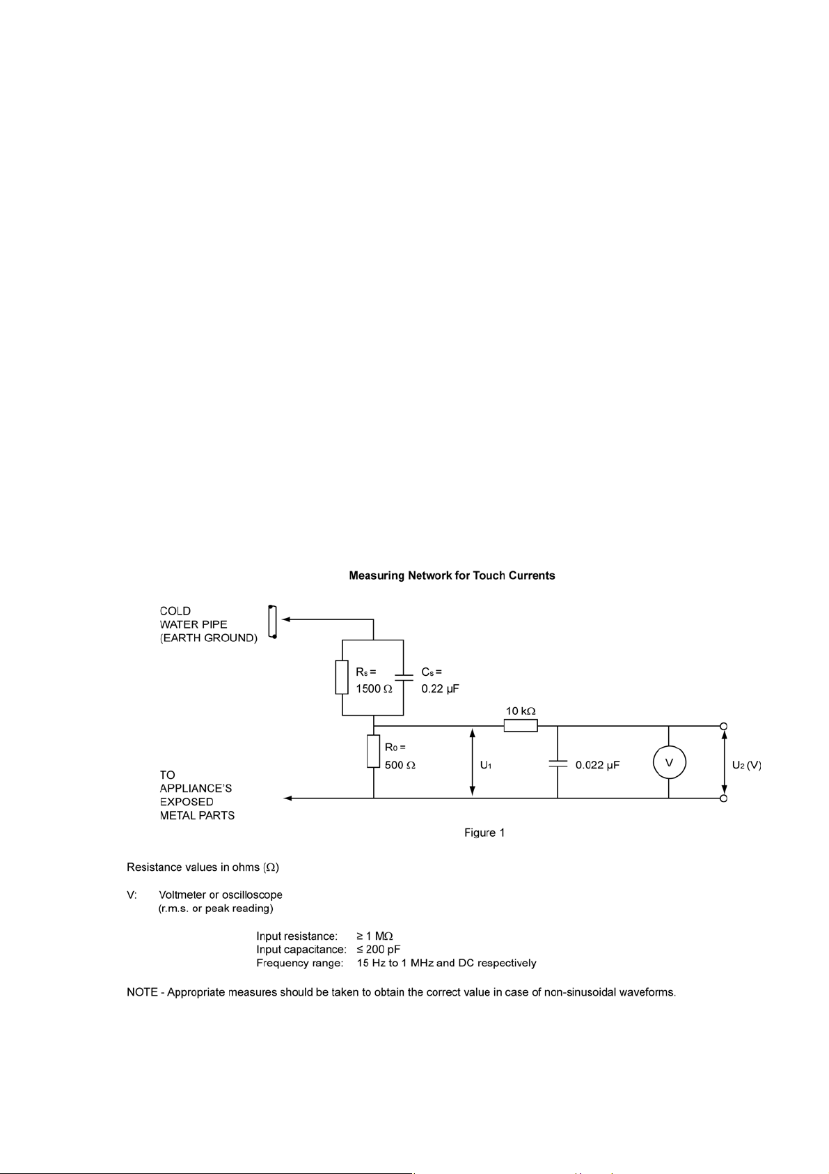
1.2. Touch-Current Check
1. Plug the AC cord directly into the AC outlet. Do not use an isolation transformer for this check.
2. Connect a measuring network for touch currents between each expo sed metallic part on the set and a good earth ground
such as a water pipe as shown in Figure 1.
3. Use the Leakage Current Tester (Simps on 228 or equivalent) to measure the potential across the measuring network.
4. Check each exposed metallic part and measure the voltage at each point.
5. The potential at any point (touch current) expressed as voltage U
For AC: U1 = 35 V (peak) and U2 = 0.35 V (peak);
For DC: U
NOTE :
The limit value of U
DC.
The limit value U
= 1.0 V,
1
= 0.35 V (peak) for AC and U1 = 1.0 V for DC correspond to the values 0.7 mA (peak) AC and 2.0 mA
2
= 35 V (peak) for AC correspond to the value 70 mA (peak) AC for frequencies greater than 100 kHz.
1
and U2, do not exceed the following values:
1
6. Should a measurement be out of the li mits specified, there is a possibility of a shock hazard , and the equipment should be
repaired and rechecked before it is returned to the customer.
5
TH-L32X10M
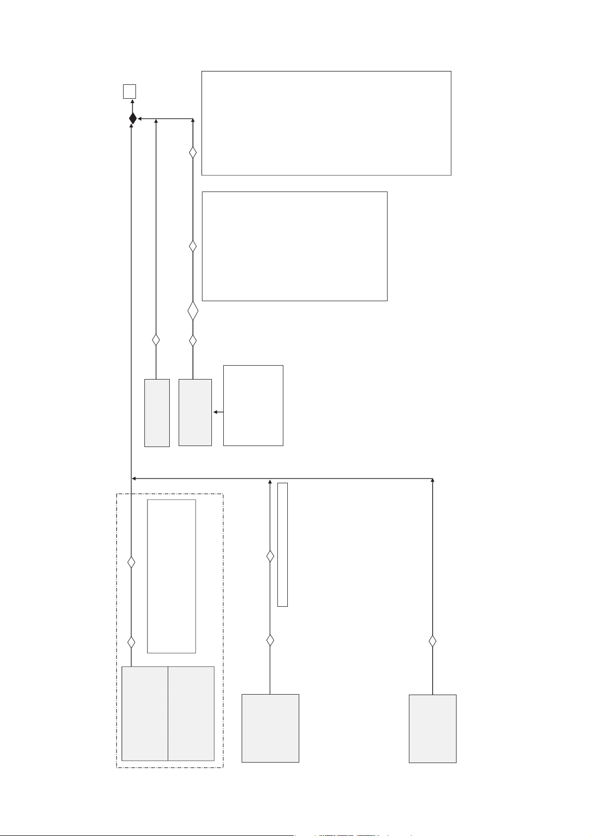
BT → Divide
A
LCD PANEL
IPK
Point Dip
Inspection
<Visual check>
*Voltage check
* LED Check Inverter (Blue LED)
<FACT-TEST>
*ANALOG TUNE
*VCXO ADJ
*LOCAL OSD
*AV_SW CHECK
*AV1/AV2/AV3---CVBS
*AV3---S(YC)
*MONITOR-OUT
*AV1/AV2---Component
*PC
*HDMI1
*HDMI2
*CEC_(HDMI1/HDMI2)
*Backlight
*SD Card
*Software & EEPROM version
check by self check (1 set only)
IP-PCB: 32” IPS ONLY
(Inverter & Power)
TNP4G455
P-PCB: 37” ONLY
(Power)
TNP4G454
BT → Divide
In coming check
Writing
Assembly
A-PCB
TNP4G460
(Degital main)
V-PCB
(LED)
TNPA4834
PEAKS NOR Flash
(Writing IC)
256Mbit
IC8554
Sum : only effective area
Add : 0 ~ 1FFFFFF
EEPROM Writing (On board)
*GENX
• EEPROM (8k) x 1
IC1101
*PEAKS
• EEPROM (16k) x 1
IC8601
<Write Protect command>
*GENX : Protect OFF = 70,88,00
Protect ON = 70,88,ff
*PEAKS : Protect OFF = 70,8B,00
Protect ON = 70,8B,ff
K-PCB
(Control)
TNPA4901
BT Inspection
FOR TNP4G455 ONLY
*Adjust the frequency to 56 ± 1kHz by using VR7851
*Check to the output : J102 or TP7871
*Check to the Over Voltage protection
*Check to the Arc protection
Inspection
LED CAT EYES,REMOCON RECEIVER
1.3. KM02 Chasis Block Diagram
6
TH-L32X10M
2 Prevention of Electro Static Discharge (ESD) to
Electrostatically Sensitive (ES) Devices
Some semiconductor (solid state) devices can be damaged easi ly by static electricity. Such components commonly are
called Electrostatically Sensitive (ES) Devices. Examples of typical ES devices are integrated circuits and s ome fieldeffect transistors and semiconductor “chip” components. The following techniques should be used to help reduce the
incidence of component damage caused by electro static discharge (ESD).
1. Immediately before handling any semiconductor component or semiconductor-equipped assembly, drain off any ESD on your
body by touching a known earth ground. Alternatively, obtain and wear a commercially available discharging ESD wrist strap,
which should be removed for potential shock reasons prior to applying power to the unit under test.
2. After removing an electrical assembly equipped with ES devices, place the assembly on a conductive surface such as
aluminium foil to prevent electrostatic charge buildup or exposure of the assembly.
3. Use only a grounded-tip soldering iron to solder or unsolder ES devices.
4. Use only an anti-static solder removal device. Some solder removal devices not classified as “anti-static (ESD protected)” can
generate electrical charges sufficient to damage ES devices.
5. Do not use freon-propelled chemicals. These can generate el ectrical charges sufficient to damage ES devices.
6. Do not remove a replacement ES device from its protective package until immediate ly before you a re ready to install it (most
replacement ES devices are packaged with leads electrically shorted together by conductive foam, aluminium foil or
comparable conductive material).
7. Immediately before removing the protective material from the leads of a replacement ES device, touch the protective material
to the chassis or circuit assembly into which the device will be installed.
Caution:
Be sure no power is applied to the chassis or circuit, and observe all other safety precautions.
8. Minimize bodily motions when handling unpackaged replacement ES devices (otherwise harmless motion such as the
brushing together of your clothes fabric or the lifting of your foot from a carpeted floor can gen erate static electricity (ESD)
sufficient to damage an ES device).
7
TH-L32X10M
3 About Lead Free Solder (PbF)
Note: Lead is listed as (Pb) in the periodic table o f elements.
In the information below, Pb will refer to Lead Solder and PbF will refer to Lead Free Solder.
The Lead Free Solder (PbF) used in our manufacturing proce ss and discussed below is (Sn+Ag+Cu).
Those are Tin (Sn), Silver (Ag) and Copper (Cu), although other types are available.
This model uses PbF in its manufacture due to environmental conservation issues. For service and repair work, we would suggest
the use of PbF as well, although Pb may be used.
PCBs manufactured using lead-free will have the “PbF within a leaf Symbol” stamped on their back.
Caution
• PbF has a higher melting point than that of standard solder. Typi cally the melting point is 50 ~ 70°F (30~40 °C) higher.
Please use a high temperature soldering iron and set it to 700 ± 20°F (370 ± 10°C).
• PbF will tend to splash when heated too high (about 1100°F or 600°C).
If you must use Pb solder, please completely remove all of the PbF on the pins or solder area before applying Pb. If this is no t
practical, be sure to heat the PbF until it melts, before applying Pb.
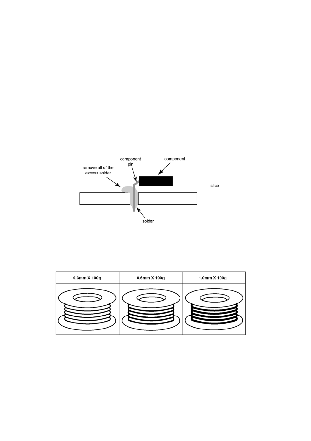
• After applying PbF to double layered boards, please check the component side for excess solder which may flow onto the
opposite side (see Figure 2).
Figure 2
Suggested PbF
There are several kinds of PbF available for purchase. This product uses Sn+Ag+C u (tin, silver, copper) solder. However, Sn+Cu
(tin, copper) and Sn+Zn+Bi (tin, zinc, bismuth) solders can also be used.
Figure 3
8
TH-L32X10M
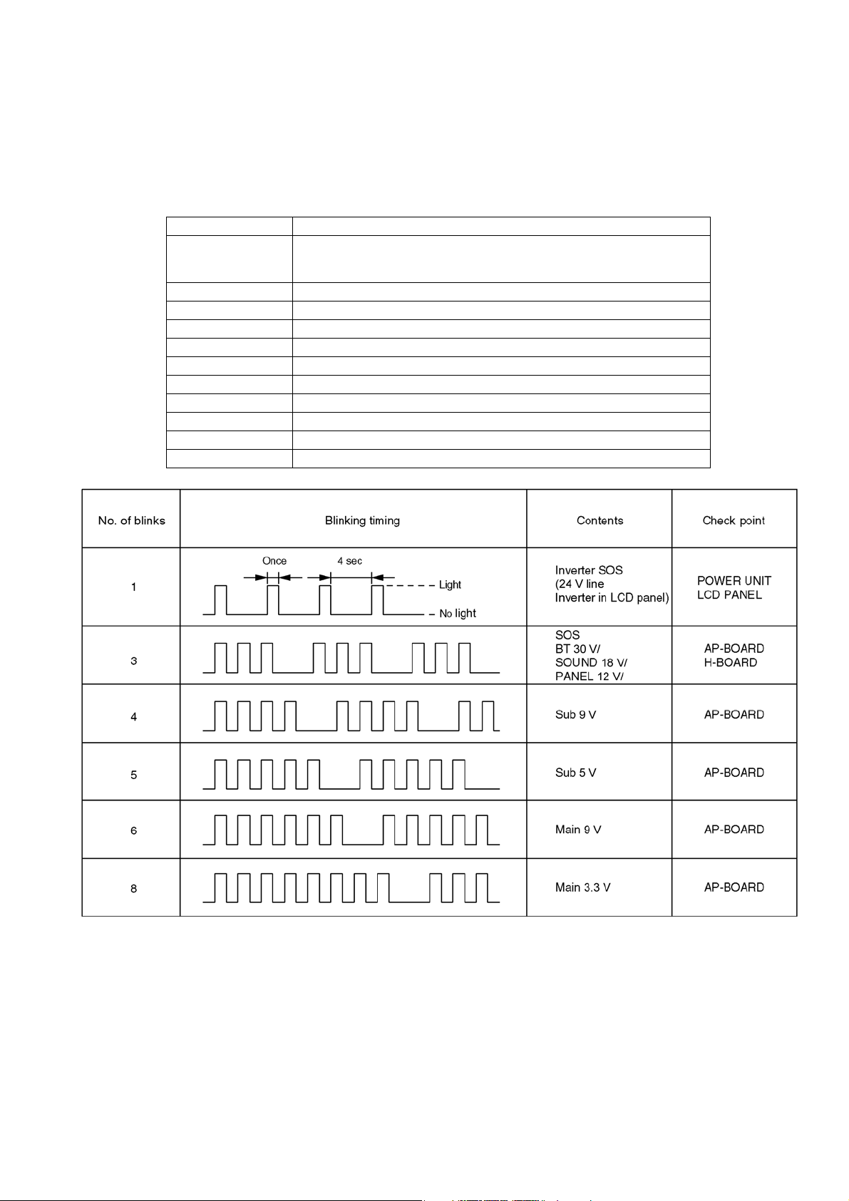
4 Power LED Blinking Timing
1. Subject
Information of LED Flashing timing.
2. Contents
When an abonormality has occurred in the unit, the protection circuit operates and resets to standby mode. At this time, the
defective block can be identified by the number of blinking of the Power LED on the front panel of the unit as follow:
Blinking times Contents
1 Lamp short circuit protection
2 Cooling fan SOS = incomplete connection - no function mode.
3 P board 30V / 18V / 9V decreased / short circuit detection.
4 DTV12V decreased / short circuit , main convertor stop detection.
5 Sub 5V decreased / short circuit detection.
6 Sub 5V decreased / short circuit detection. (same as 5 times LED blinking)
7 Sub 3.3V decreased / short circuit detection.
8 Sub 5V decreased / short circuit detection. (same as 5 times LED blinking)
9 Audio amp SOS.
10 HQ1 incomplete connection, no function mode.
13 When peaks communication error SOS.
Lamp open protection
Arc protection
9
TH-L32X10M
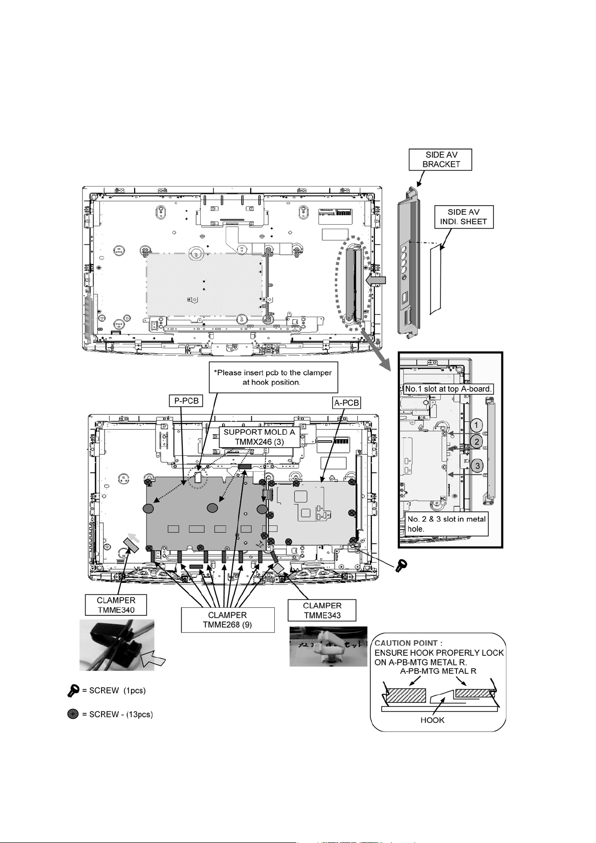
5 Chassis Board
5.1. Chassis Installation
1. Stick FELT to SIDE AV BRACKET.
- Stick the SIDE AV INDI. SHEET on the SIDE AV BRACKET.
- Insert the SIDE AV BRACKET from the side position of the A-PCB.
10
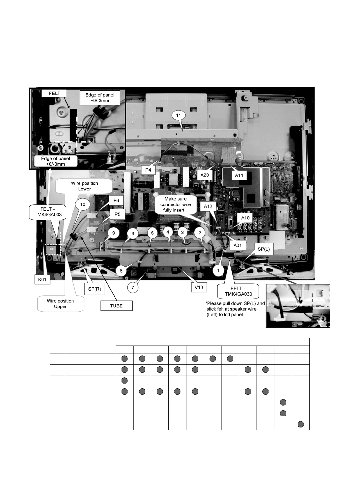
6 Location of Controls and Components
6.1. Wire Dressing
1. Wiring No. 1 ~ No.7
2. Remove dust of terminal of LVDS and PB connector. (by ion blow) Pos. A11
3. Insert LVDS into A11.
TH-L32X10M
Wire
No.1 A10 ~ V10
No.2 A01 ~ K01
No.3 A12 ~ SP(L)
No.4 A12 ~ SP(R)
No.5 ~ P5
No.6 ~ P6
No.7 A20 ~ P4
Clamper
1234567891011
11
TH-L32X10M
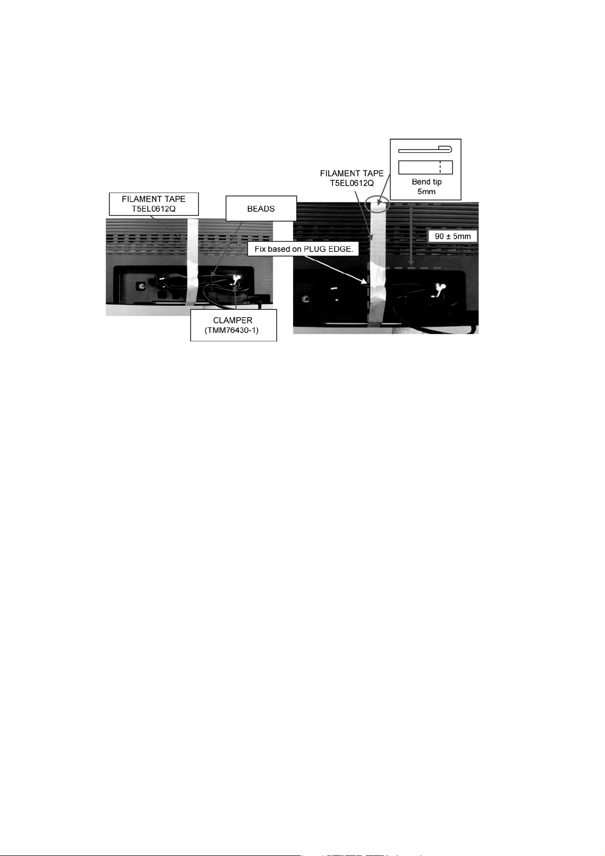
7 Disassembly and Assembly Instructions
7.1. AC Cord Dressing
1. Clamp plug with clamper.
2. Insert beads 3pcs. And slide down to lower hole.
12
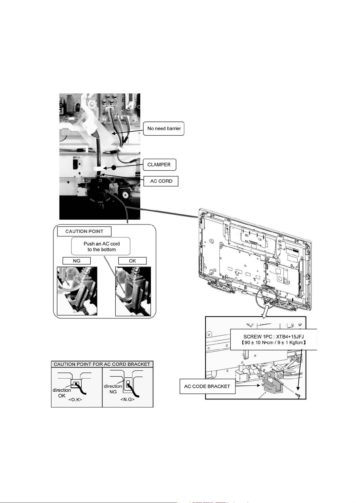
7.2. AC Cord Installation
1. Put on the AC CORD BRACKET on the CABINET.
2. Fix the AC CORD BRACKET with SCREW.
3. AC CORD BARRIER setting.
4. Insert AC CORD connector into P-PCB connector.
5. Clamp the AC CORD.
6. Insert AC CORD bushing into the AC CORD BRACKET.
TH-L32X10M
13
TH-L32X10M
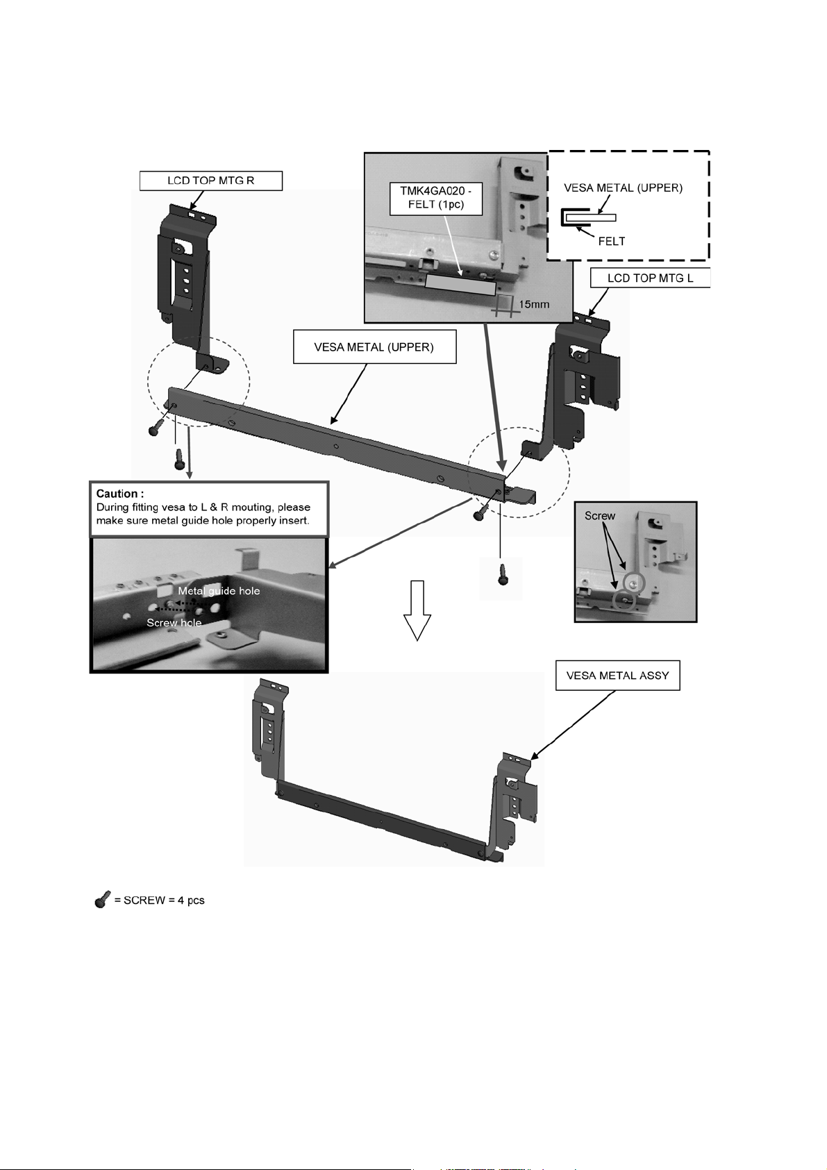
7.3. VESA Metal Assembly
1. Assemble LCD TOP MTG(L,R) , VESA METAL(upper) and fix them with screw. Please use jig for vesa metal assembly
preparation.
14
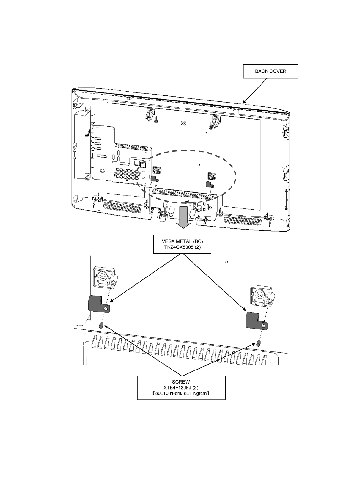
7.4. VESA (BC) Installation
1. Put VESA METAL(BC) on the BACK COVER.
2. Fix them with SCREWS.
TH-L32X10M
15

TH-L32X10M
7.5. Pedestal Assembly
Step 1
Setting PEDESTAL COVER and STAND MTG SPACER and BASE PLATE with SCREWS.
Step 2
1. Stick the RUBBER FOOT at bottom ROTATION PLATE.
2. Make sure ROTATION PLATE surfacefully cover by grease. Follow the picture
16
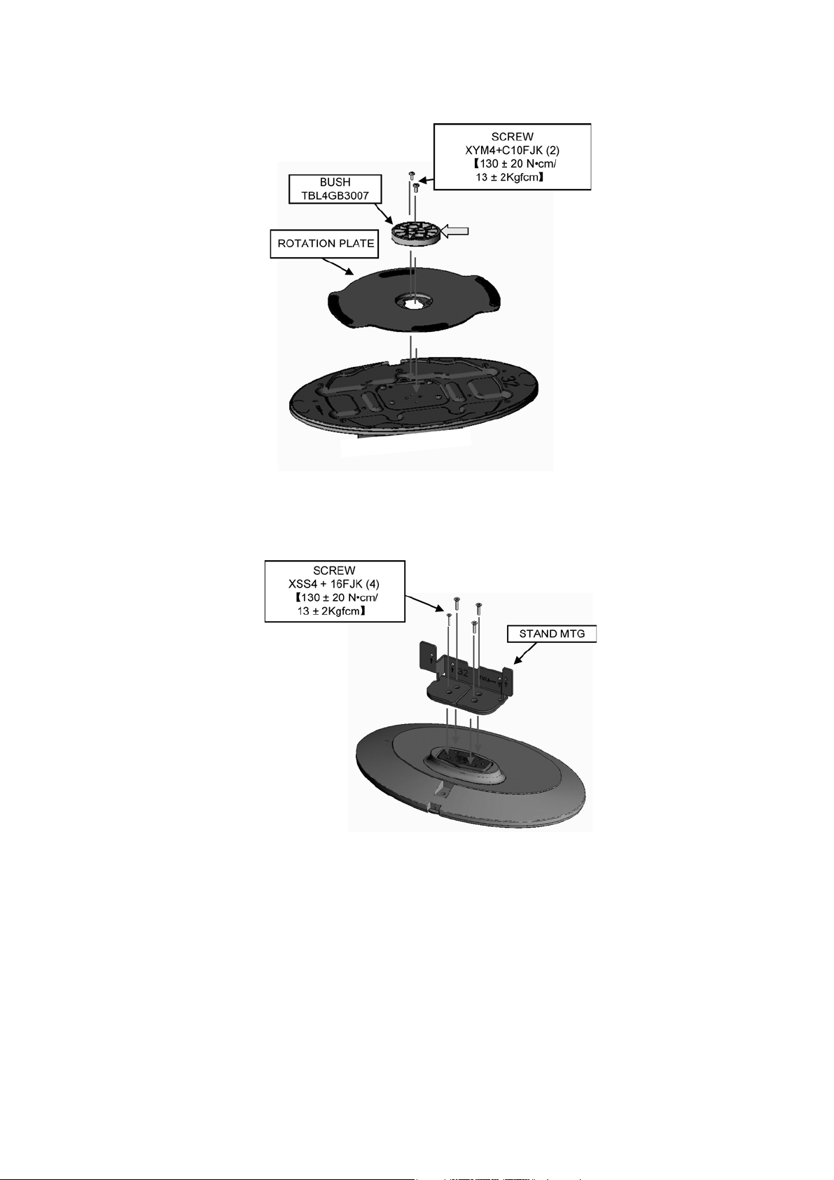
Step 3
Setting ROTATION PLATE and BUSH with SCREWS.
TH-L32X10M
Step 4
Setting STAND MTG with SCREWS.
17
TH-L32X10M
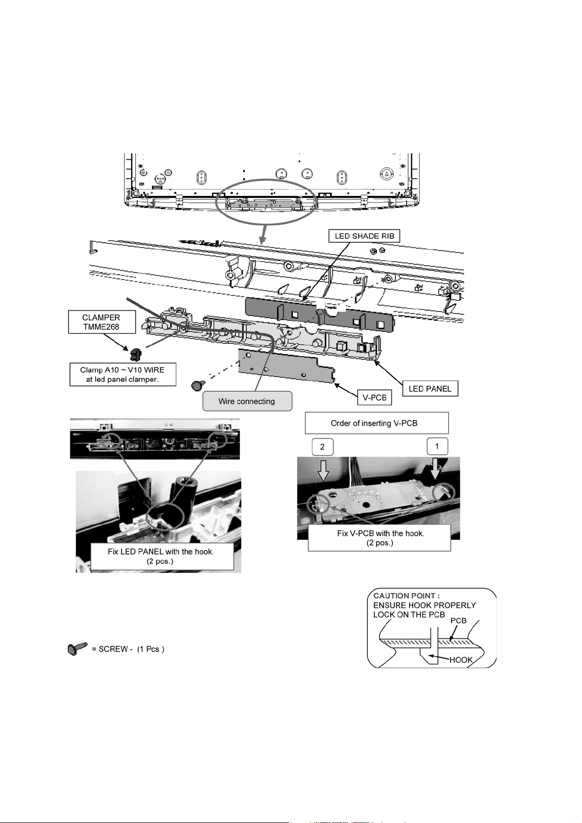
7.6. LED Panel Installation & Fitting
1. Put LED SHADE RIB on CABINET.
2. Fix LED PAN E L on CABINET.
3. Wire connecting. (V10)
4. Put V-PCB on CABINET.
5. Fix them with SCREW.
6. Insert the CLAMPER.
18

7.7. Control Panel Assembly
1. Wire connecting. (K1)
2. Assemble POWER BUTTON to the K-PRINT.
3. Assemble K-PRINT, CONTROL BUTTON, CONTROL PANEL BRACKET.
4. Fix them with SCREWS.
5. Stick the FELT.
TH-L32X10M
19
TH-L32X10M
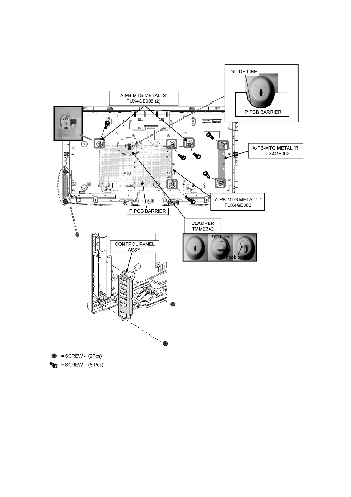
7.8. A-PB-MTG & Control Button Fixing
1. Stick P-PCB BARRIER and put all METAL part follow to the picture.Fix all metal part with screw.
2. Put CONTROL PANEL ASSY on the CABINET. Fix the CONTROL PANEL with SCREWS.
20
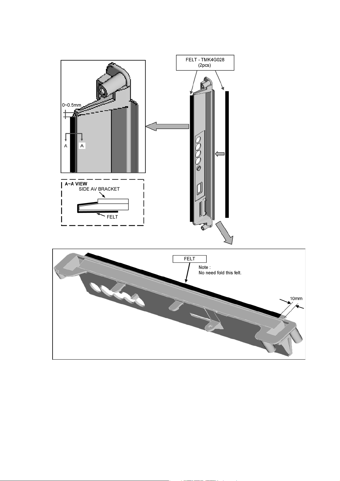
7.9. Side AV Bracket Assembly
• STICK FELT TMK4G028 (7 X 240 X 0.55t) - 2 PCS.
TH-L32X10M
21
TH-L32X10M
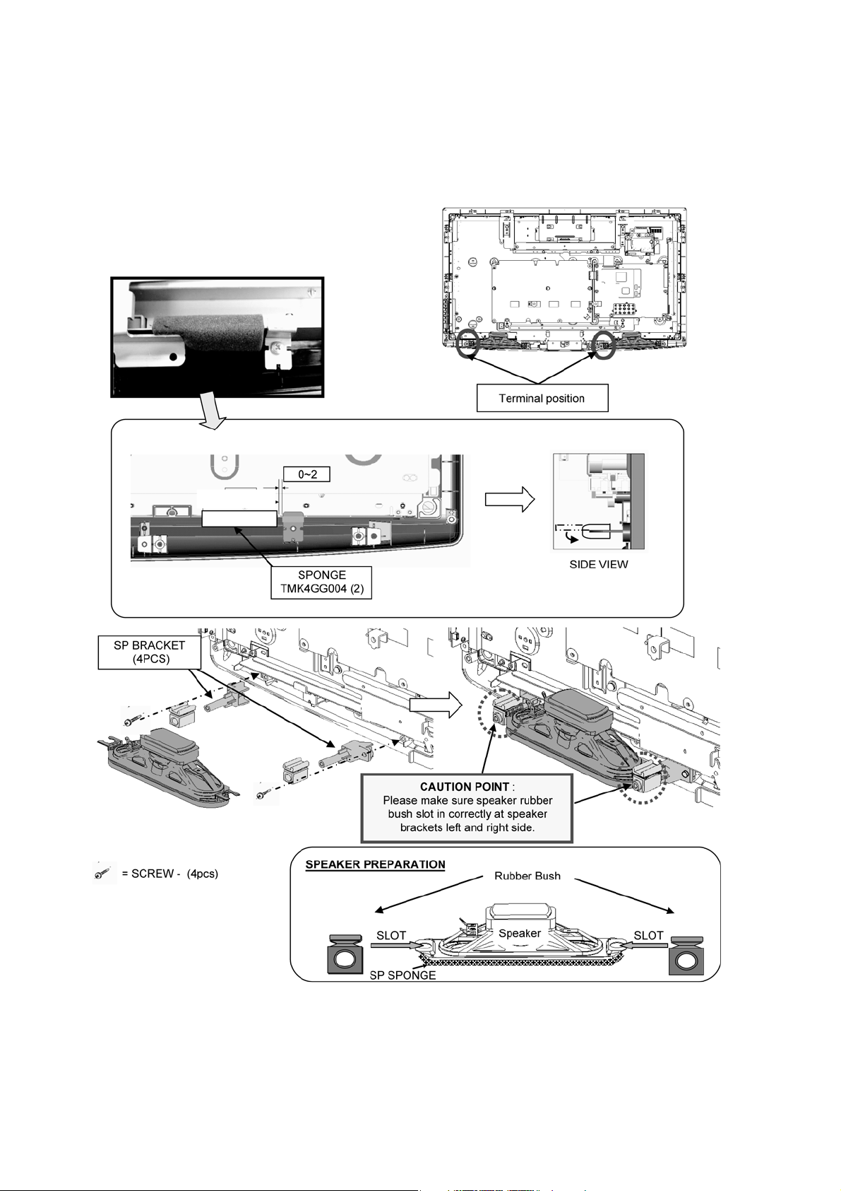
7.10. Speaker Installation
1. Stick the SPONGE. Follow the spec. below.
2. SP BRACKET slot at CABINET.
3. Insert the SP RUBBER BUSH into the SP UNIT.
4. Insert the SP UNIT to SP BRACKET.
5. Fix them with SCREWS.
22
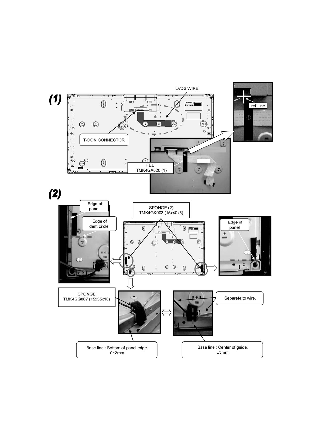
7.11. LCD Panel
1. Remove dust of terminal of LVDS. (by ion blow)
2. Remove dust of terminal of T-con connector. (by ion blow)
3. Insert LVDS into T-con connector.
4. Stick the tape to fix LVDS.
5. Stick the SPONGE at left and right lcd panel.
6. Stick 1pc SPONGE between lcd panel wire.
TH-L32X10M
23
TH-L32X10M
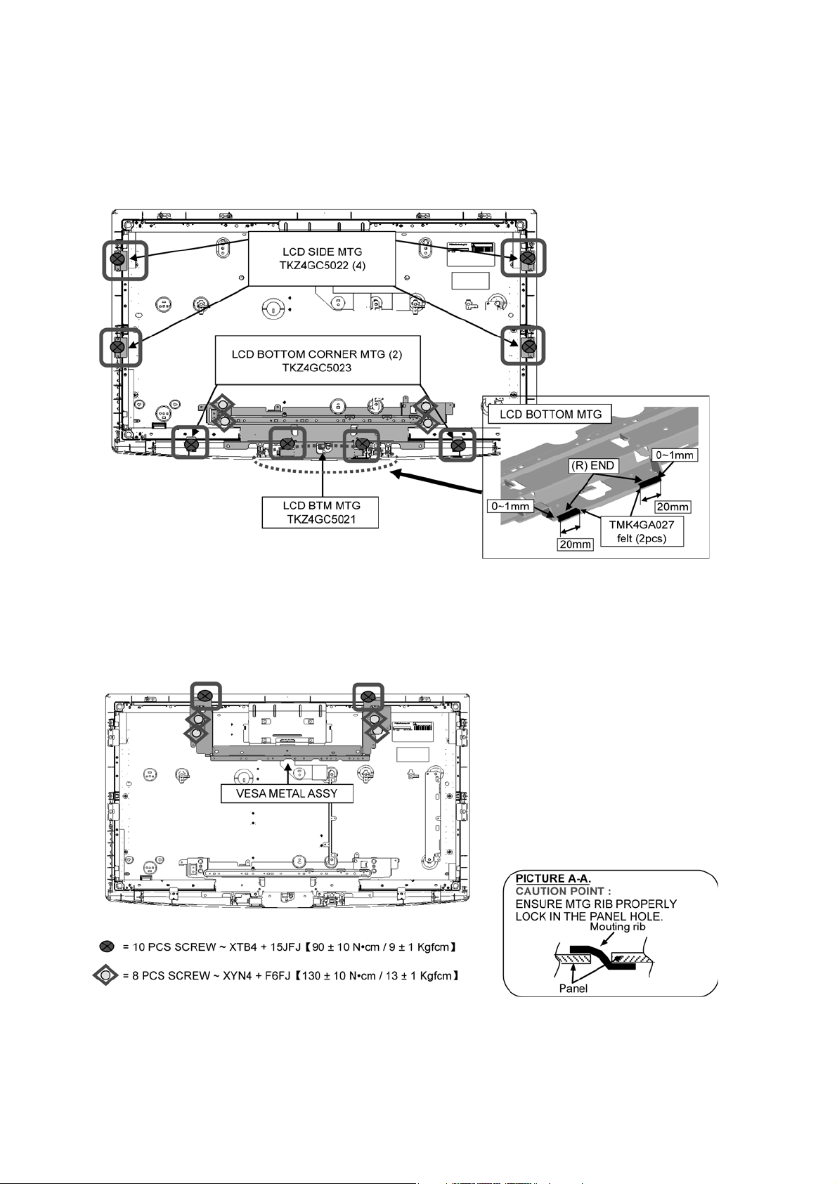
7.12. LCD Mouting Fixing
Step 1
1. LCD SIDE MTG on the CABINET.
2. LCD BTM MTG on the CABINET.
3. LCD BOTTOM CORNER MTG on the CABINET.
4. Fix them with SCREW.
Step 2
1. Assemble LCD TOP MTG (L, R), VESA METAL (upper) and fix them with SCREWS.
2. Put on the VESA METAL ASSY on the LCD PANEL.
3. Fix the VESA METAL ASSY with SCREW.
24
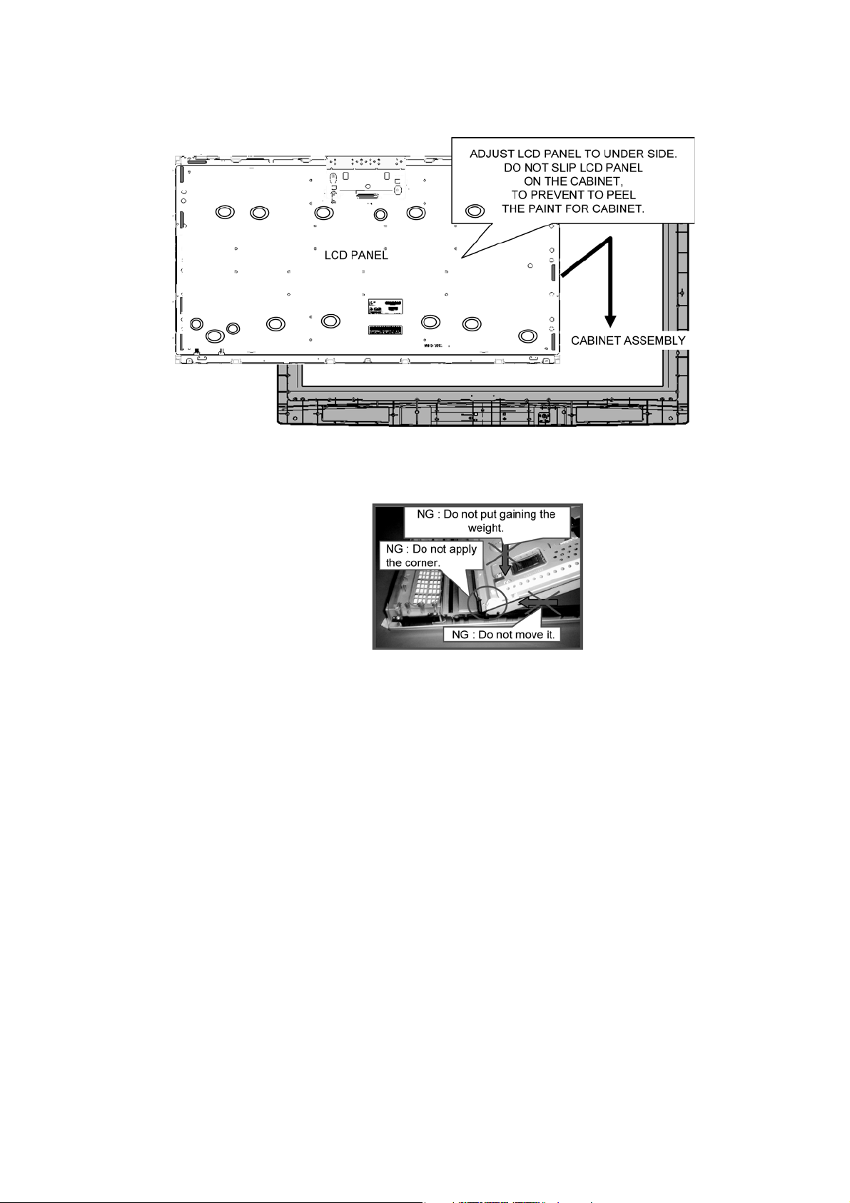
7.13. LCD Panel Assembly Installation
1. Put LCD panel to cabinet assembly.
TH-L32X10M
25
TH-L32X10M
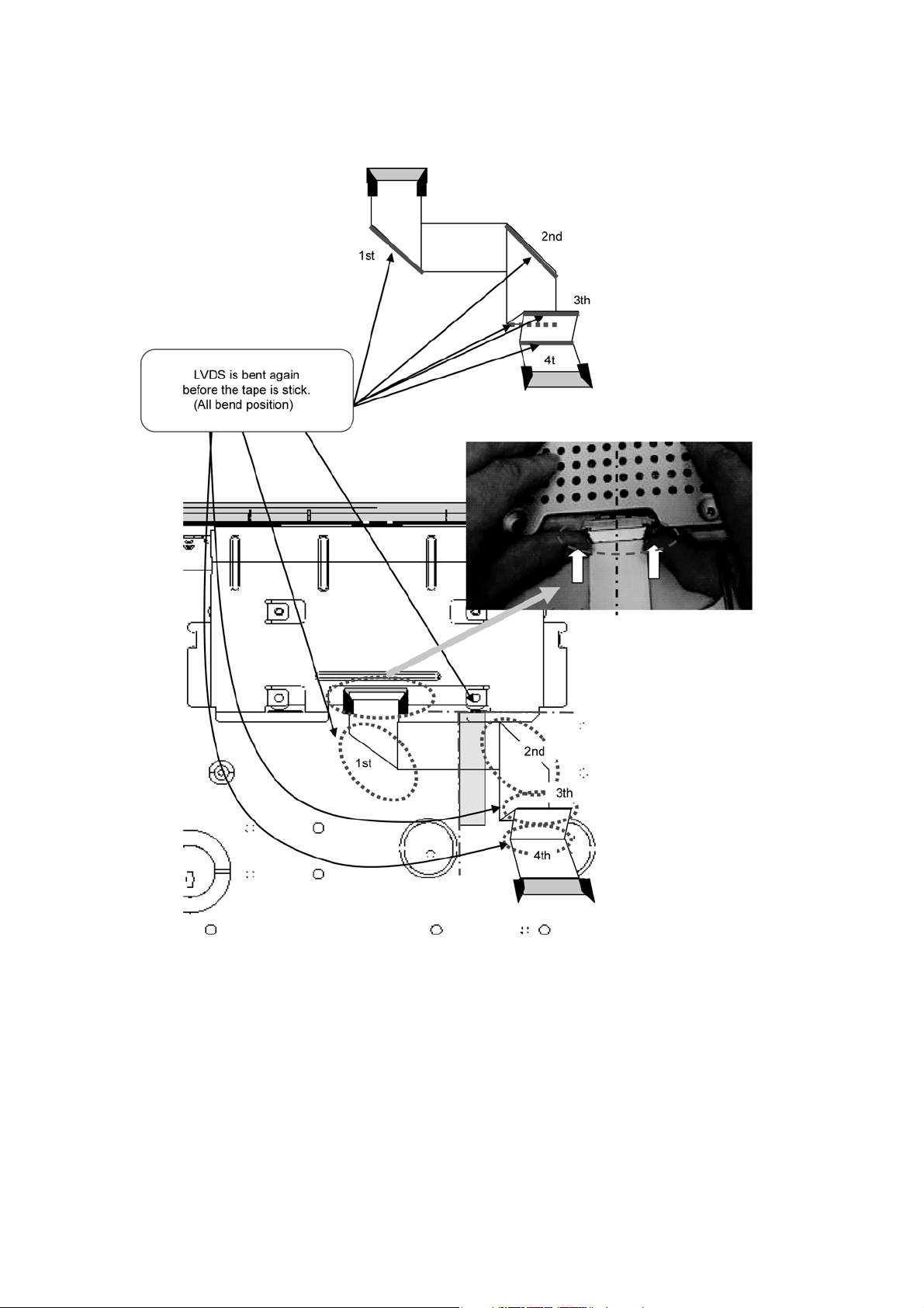
7.14. EMI Spec (LVDS)
1. When insert LVDS wire to T-con conector,make sure must center position follow bellow picture.
2. After fixing LVDS wire please bent again follow the picture.
26
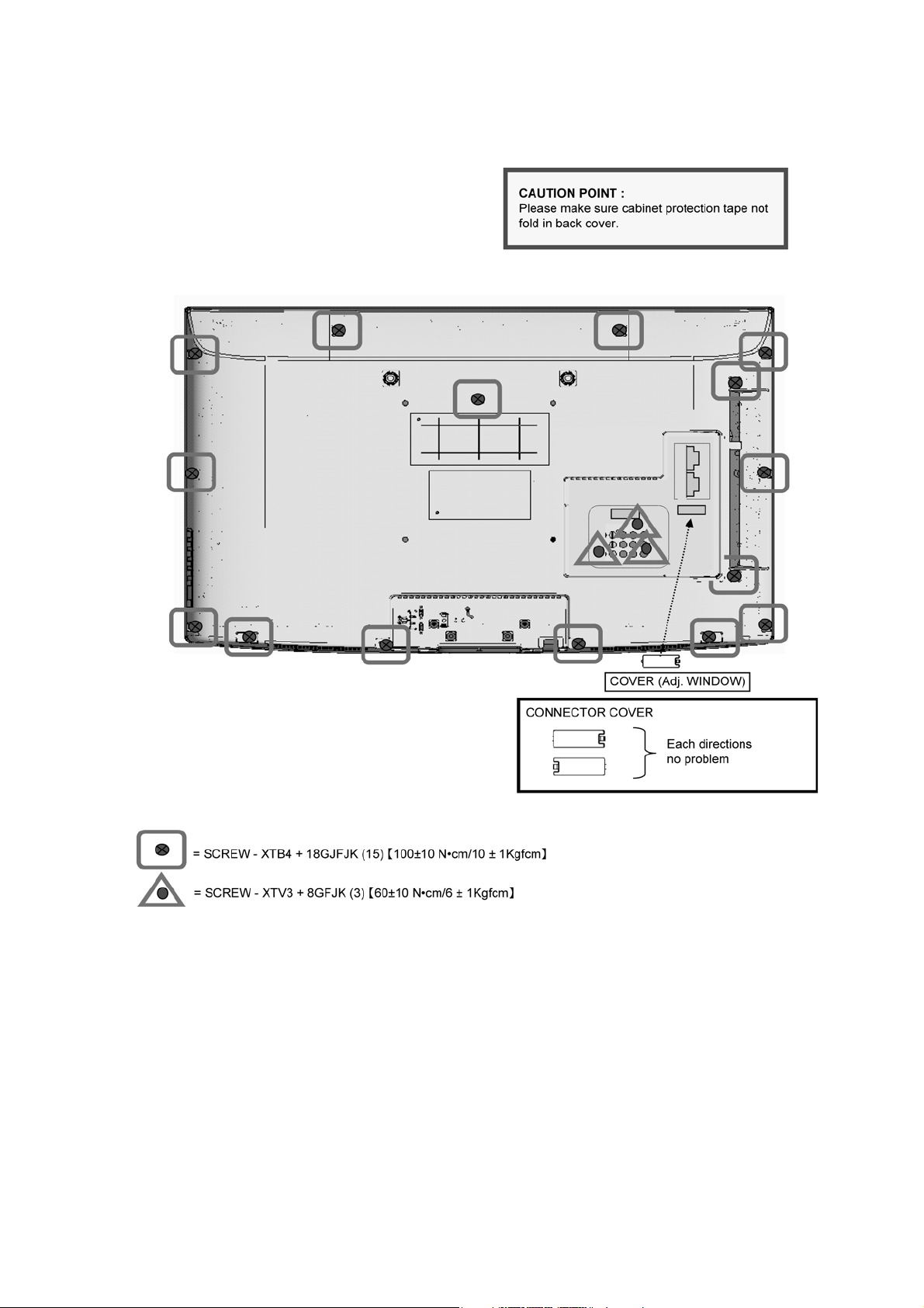
7.15. Back Cover Screw
1. Fix the BACK COVER with SCREWS.
2. Insert COVER (Adj.window).
TH-L32X10M
27
TH-L32X10M
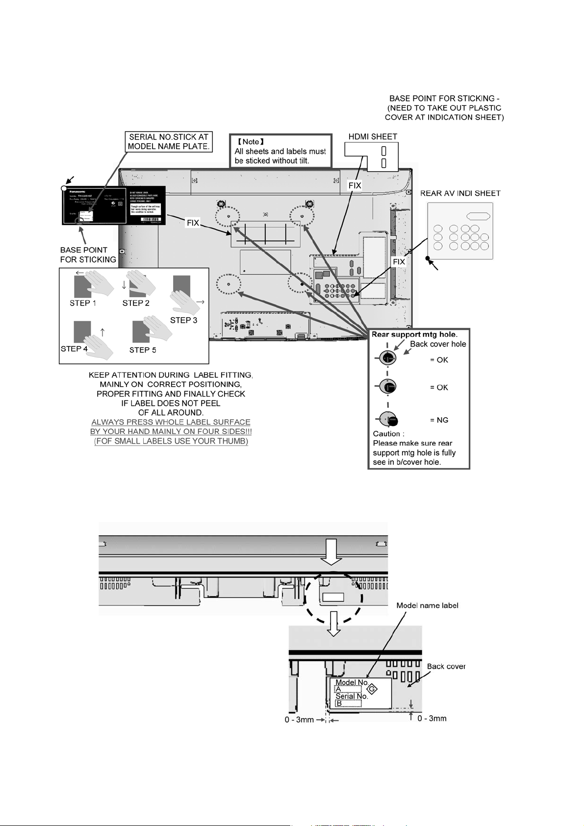
7.16. Indication Sheet Sticking Position
Stick the HDMI/REAR AV/MODEL NAME SHEET .
Stick model no. at bottom back cover (Stick area no etching).
28
TH-L32X10M
8 Service Mode Adjustment
Set timer to 30min, press the “RECALL” button on the remote control and press “-” vol button on the LCD panel.
• Press button R and G for adjustment.
8.1. Self Check Mode
1. Press the “MENU” button (on the remote control ) and the “DOWN” button on the LCD panel.
2. Press ON/OFF button on the panel to Exit.
8.2. Hotel Mode Adjustment
1. Press the “VOLUME DOWN” button on the TV panel and simultaneously press the AV button on the remote control 3 times to
enter Hotel Mode.
2. Set Hotel mode “on”, then press “EXIT” to come out.
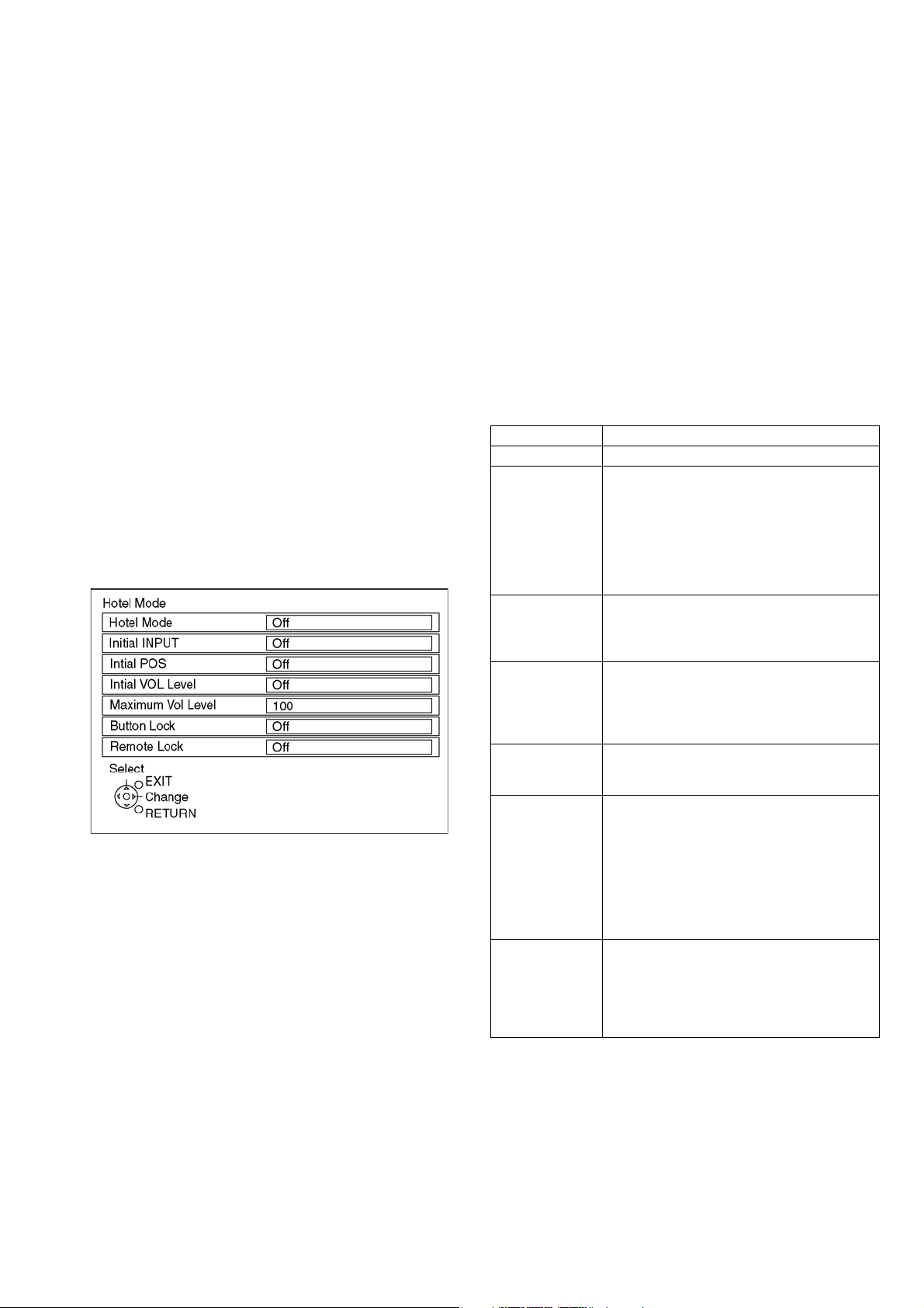
8.3. Hotel Mode
1. Purpose
Restrict a function for hotels.
2. Access command to the Hotel mode setup menu.
In order to display the Hotel mode setup menu, please
enter the following command (within 2 second).
[TV] : Hold Vol [Down] + [Remote] : Press AV button 3
times.
Then, the Hotel mode setup menu is displayed.
Item Function
Hotel Mode Select hotel mode ON/OFF
Initial INPUT Select input signal modes.
Set the input, when each time power is switched
on.
Selection :
OFF/Analogue TV/Digital TV/AV1/AV2/AV3//PC/
HDMI1/HDMI2/HDMI3
• Off: give priority to a last memory.
• Selectable input is depend on the model.
Initial POS Select programme number.
Selection :
Off/0 to 100
• Off: give priority to a last memory.
Initial VOL level Adjust the volume when each time power is
switched on.
Selection/Range :
Off/0 to 100
• Off: give priority to a last memory.
Maximum VOL
level
Button lock Select local key conditions.
Remote lock Select remote control key conditions.
Adjust maximum volume.
Range :
0 to 100
Selection :
Off/SETUP/MENU/All
• Off: altogether valid.
• SETUP: only F-key is invalid.
(Tuning guide (menu) can not be selected.)
• MENU: only F-key is invalid.
(only Volume/Mute can be selected.)
• ALL: altogether invalid.
Selection :
Off/SETUP/MENU
• Off: altogether valid.
• SETUP: only Setup menu is invalid.
• MENU: Picture/Sound/Setup menu are invalid.
29
TH-L32X10M
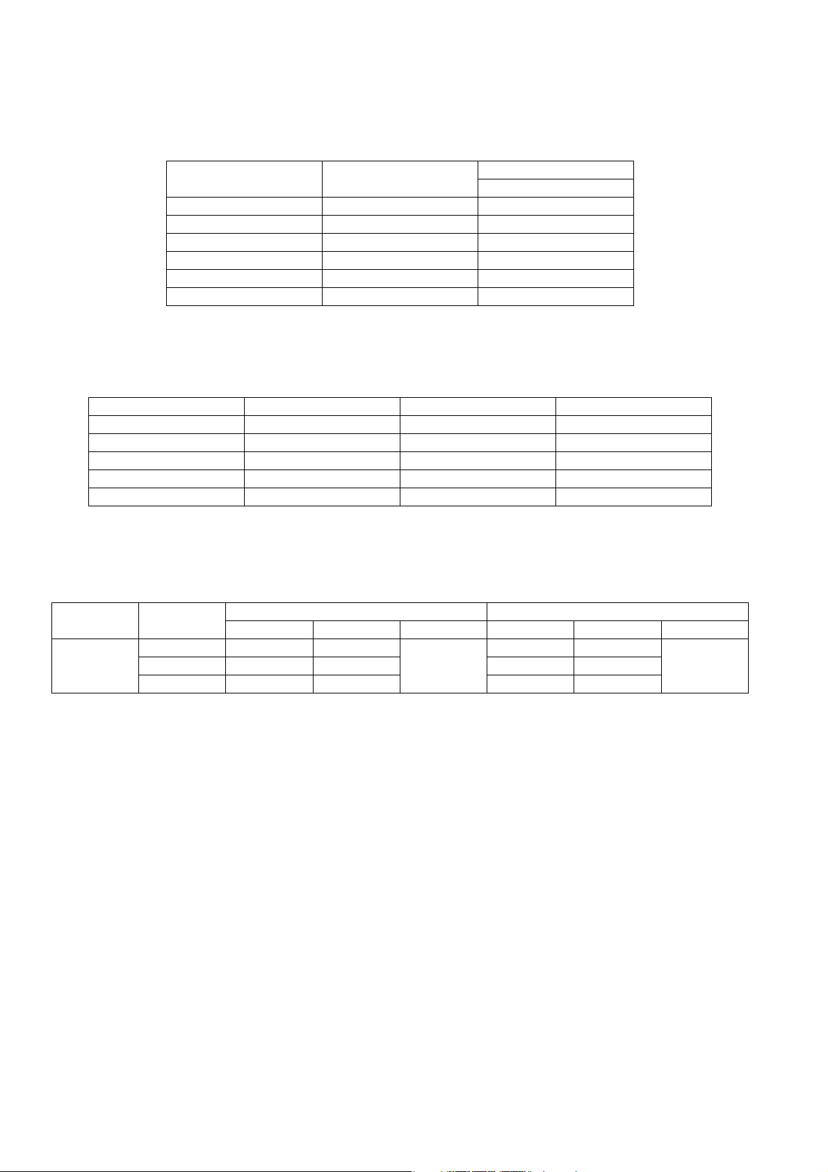
9 Measurements and Adjustments
9.1. Voltage Chart of A Board
Set A-Board to a dummy set and check the satisfaction with the specified voltage as following table.
Power Supply Name Measurement Point
SUB1.2V TP5602 1.22 - 1.32
SUB1.8V TP5601 1.78 - 1.91
SUB3.3V TP5600 3.21 - 3.45
SUB9V TP5409 8.76 - 9.45
SUB5V TP5405 4.82 - 5.18
BT30V TP5482 29.3 - 31.5
Specification (V)
TNP4G460 / TNP4G461
9.2. Voltage Chart of P Board
Set P-Board to a dummy set and check the satisfaction with the specified voltage as following table.
Power Supply name Measurement Point Normal condition (V) Standby condition (V)
AUDIO_VCC TP866 17.0 ± 1.7 < 3.0
12V TP865 12.0 ± 0.6 < 1.0
5VS TP854 5.6 ± 0.3 5.6 ± 0.3
STBY_6V TP853 5.6 ± 0.3 5.6 ± 0.3
PFC Vout TP801 400 ± 10 NO CARE
After inspection, discharge the C7218 with 1kΩ resistor for 0.3 sec. or more.
9.3. Target of White Balance adjustment value
Ambient Temp. Colour Balance
Cool 0.271 0.275
22.5 - 27.5 deg.
Warm 0.314 0.324 0.314 0.324
x y Y (cd/m2) x y Y (cd/m2)
Clearance
x, y : +/-0.005 in Cool Colour Balance, +/-0.010 in Warm/Normal Colour Balance
White Gray
>300
0.271 0.275
Don’t CareNormal 0.284 0.297 0.284 0.297
30
 Loading...