

Page 1
ORDER NO. MTV1001917CE
LCD TV
Model No.
TH-L32A20X
Chassis: KM06
Destination: SINGAPORE
TABLE OF CONTENTS
1 Safety Precautions ----------------------------------------------- 3
1.1. General Guidelines---------------------------------------- 3
1.1.1. Leakage Current Cold Check ---------------------- 3
1.1.2. Leakage Current Hot Check (See Figure
1.) --------------------------------------------------------- 3
2 Warning-------------------------------------------------------------- 4
2.1. Prevention of Electrostatic Discharge (ESD)
to Electrostatically Sensitive (ES) Devices---------- 4
2.2. About lead free solder (PbF)---------------------------- 5
3 Service Navigation ----------------------------------------------- 6
3.1. Service Hint ------------------------------------------------- 6
3.2. Applicable signals ----------------------------------------- 7
4 Specifications ----------------------------------------------------- 8
5 Service Mode -----------------------------------------------------10
5.1. How to enter into Service Mode ----------------------10
5.1.1. Contents of adjustment mode --------------------10
5.1.2. How to exit---------------------------------------------10
5.2. SRV-TOOL -------------------------------------------------11
5.2.1. How to access ---------------------------------------- 11
PAG E PAG E
5.2.2. Display of SOS History ---------------------------- 11
5.2.3. POWER ON TIME/COUNT ----------------------- 11
5.2.4. Exit ------------------------------------------------------ 11
5.3. Service Mode Adjustment------------------------------ 12
5.3.1. Self Check Mode ------------------------------------ 12
5.3.2. Hotel Mode Adjustment ---------------------------- 12
5.3.3. Hotel Mode-------------------------------------------- 12
6 Troubleshooting Guide --------------------------------------- 13
6.1. Check of the IIC bus lines------------------------------ 13
6.1.1. How to access --------------------------------------- 13
6.1.2. Exit ------------------------------------------------------ 13
6.1.3. Screen display --------------------------------------- 13
6.1.4. Check Point ------------------------------------------- 13
6.2. Power LED Blinking timing chart --------------------- 14
6.3. No Power--------------------------------------------------- 14
7 Disassembly and Assembly Instructions--------------- 15
7.1. AC Cord Dressing---------------------------------------- 15
7.2. AC Cord Installation ------------------------------------- 16
7.3. VESA Rail Installation----------------------------------- 17
© Panasonic Corporation 2010. Unauthorized
copying and distribution is a violation of law.
Page 2

TH-L32A20X
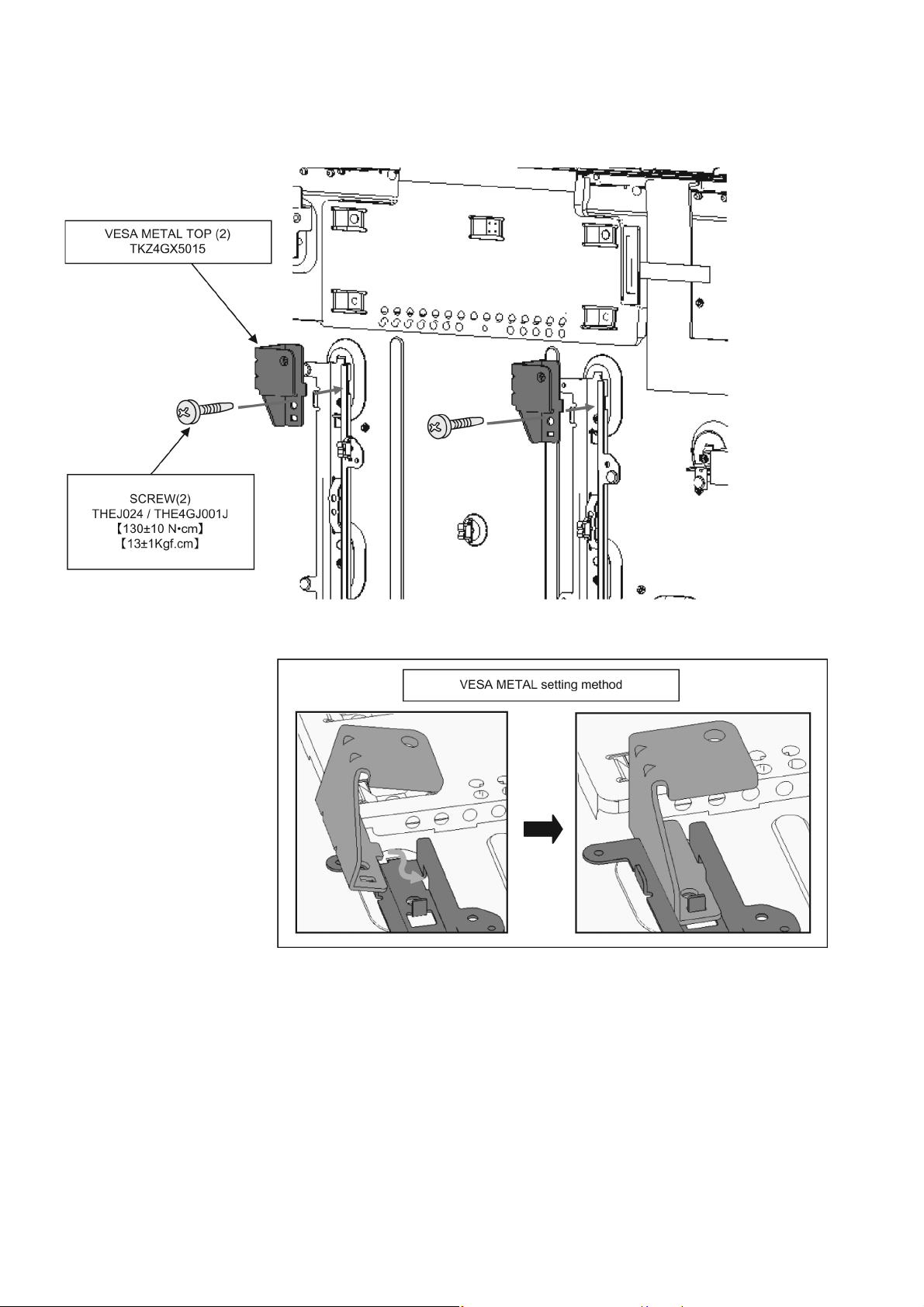
7.4. VESA Metal Assembly ---------------------------------- 18
7.5. Control Panel Assembly -------------------------------- 19
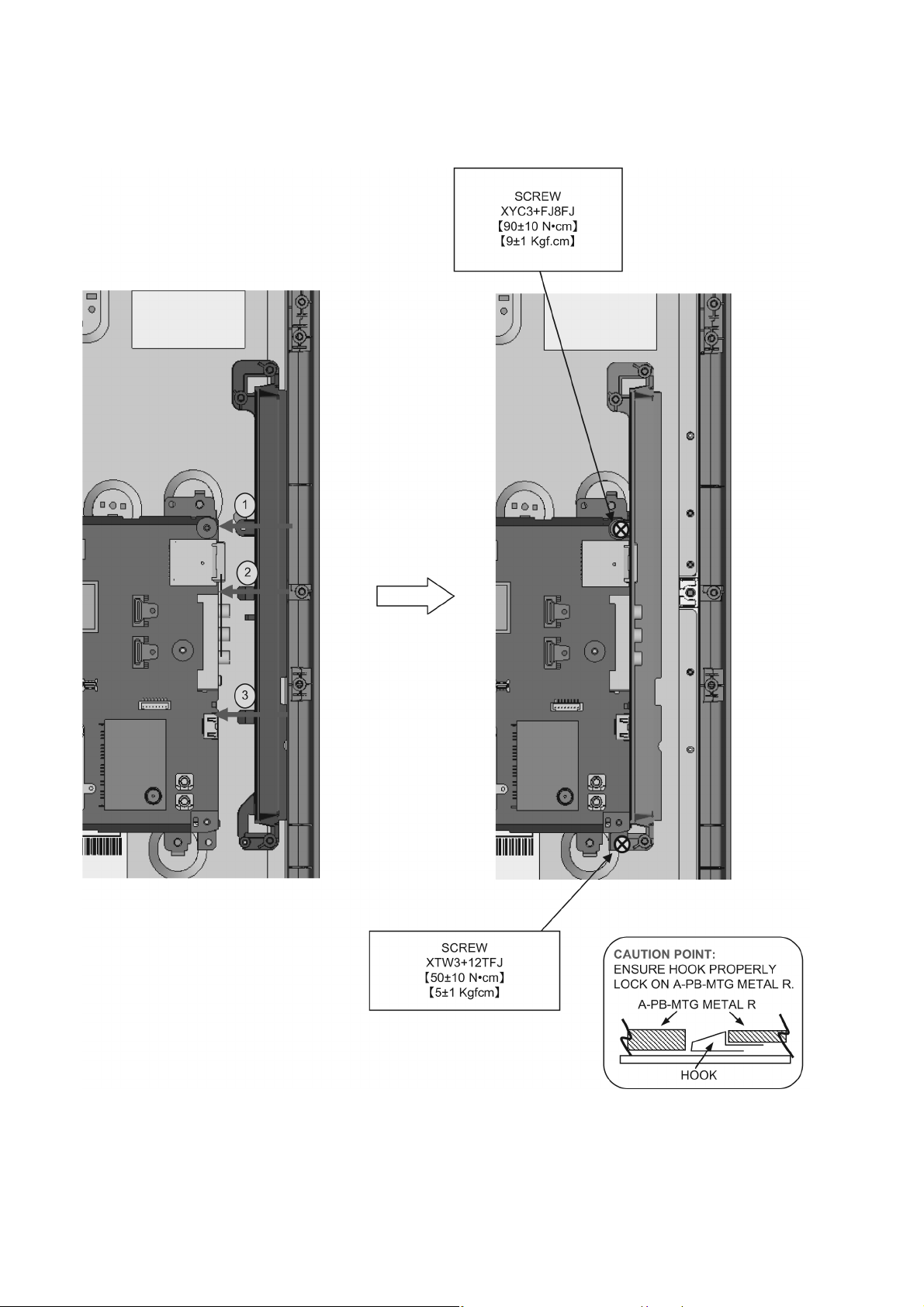
7.6. Side AV Bracket Assembly ----------------------------20
7.7. SP Installation---------------------------------------------21
7.8. LCD Panel Installation ---------------------------------- 22
7.9. LED Panel Installation & Fitting----------------------- 23
7.10. LCD Mounting Installation 1 --------------------------- 24
7.11. LCD Mounting Installation 2 --------------------------- 25
7.12. LCD Mounting Installation 3 --------------------------- 26
7.13. Metal Bracket Installation ------------------------------ 27
7.14. LVDS Installation ----------------------------------------- 28
7.15. PCB and Clamper Assembly -------------------------- 29
7.16. PB MTG Installation -------------------------------------30
7.17. Pedestal Assembly 1 ------------------------------------ 31
7.18. Pedestal Assembly 2 ------------------------------------ 32
7.19. Pedestal Assembly 3 ------------------------------------ 32
7.20. Stand MTG Assembly-----------------------------------34
8 Measurements and Adjustments -------------------------- 35
8.1. Voltage chart of A-board-------------------------------- 35
8.2. Voltage chart of P-board-------------------------------- 35
8.3. Picture level adjustment (RF) ------------------------- 35
8.4. Picture level adjustment (VIDEO) -------------------- 36
8.5. Picture level adjustment (YUV) ----------------------- 36
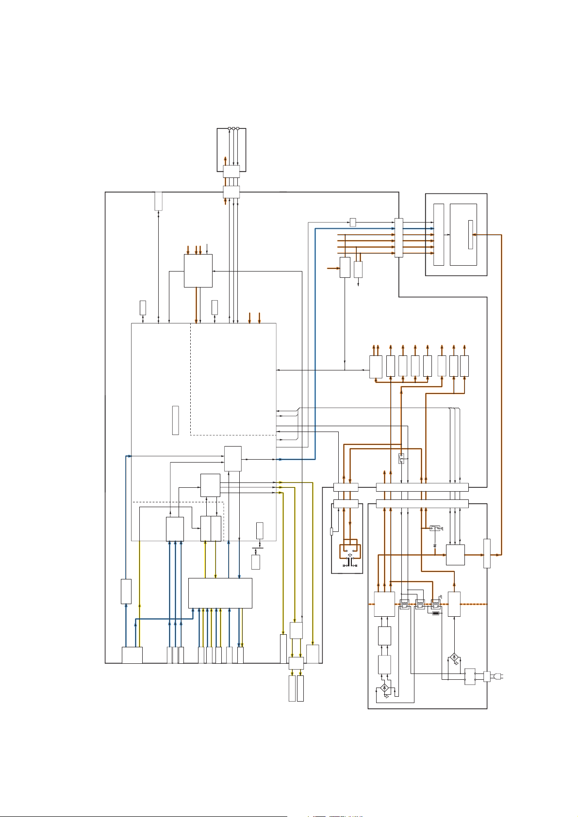
9 Block Diagram --------------------------------------------------- 37
9.1. Main Block Diagram ------------------------------------- 37
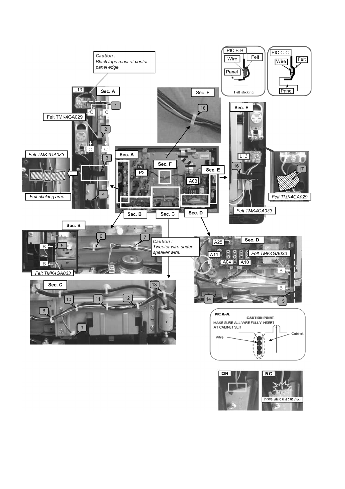
10 Wiring Connection Diagram --------------------------------- 38
11 Schematic Diagram--------------------------------------------- 40
11.1. Schematic Diagram Notes ----------------------------- 40
11.2. A Board ----------------------------------------------------- 41
11.2.1. A Board - Sheet : 002 (1 / 4)---------------------- 41
11.2.2. A Board - Sheet : 002 (2 / 4)---------------------- 42
11.2.3. A Board - Sheet : 002 (3 / 4)---------------------- 43
11.2.4. A Board - Sheet : 002 (4 / 4)---------------------- 44
11.2.5. A Board - Sheet : 003 (1 / 3)---------------------- 45
11.2.6. A Board - Sheet : 003 (2 / 3)---------------------- 46
11.2.7. A Board - Sheet : 003 (3 / 3)---------------------- 47
11.2.8. A Board - Sheet : 005 (1 / 3)---------------------- 48
11.2.9. A Board - Sheet : 005 (2 / 3)---------------------- 49
11.2.10. A Board - Sheet : 005 (3 / 3)----------------------50
11.2.11. A Board - Sheet : 007 (1 / 4)---------------------- 51
11.2.12. A Board - Sheet : 007 (2 / 4)----------------------52
11.2.13. A Board - Sheet : 007 (3 / 4)----------------------53
11.2.14. A Board - Sheet : 007 (4 / 4)----------------------54
11.2.15. A Board - Sheet : 009 (1 / 4)----------------------55
11.2.16. A Board - Sheet : 009 (2 / 4)----------------------56
11.2.17. A Board - Sheet : 009 (3 / 4)----------------------57
11.2.18. A Board - Sheet : 009 (4 / 4)----------------------58
11.2.19. A Board - Sheet : 010 (1 / 6)----------------------59
11.2.20. A Board - Sheet : 010 (2 / 6)----------------------60
11.2.21. A Board - Sheet : 010 (3 / 6)----------------------61
11.2.22. A Board - Sheet : 010 (4 / 6)----------------------62
11.2.23. A Board - Sheet : 010 (5 / 6)----------------------63
11.2.24. A Board - Sheet : 010 (6 / 6)----------------------64
11.2.25. A Board - Sheet : 012 (1 / 3)----------------------65
11.2.26. A Board - Sheet : 012 (2 / 3)----------------------66
11.2.27. A Board - Sheet : 012 (3 / 3)----------------------67
11.2.28. A Board - Sheet : 015 (1 / 4)----------------------68
11.2.29. A Board - Sheet : 015 (2 / 4)----------------------69
11.2.30. A Board - Sheet : 015 (3 / 4)----------------------70
11.2.31. A Board - Sheet : 015 (4 / 4)----------------------71
11.2.32. A Board - Sheet : 016 (1 / 4)----------------------72
11.2.33. A Board - Sheet : 016 (2 / 4) --------------------- 73
11.2.34. A Board - Sheet : 016 (3 / 4) --------------------- 74
11.2.35. A Board - Sheet : 016 (4 / 4) --------------------- 75
11.2.36. A Board - Sheet : 017 (1 / 4) --------------------- 76
11.2.37. A Board - Sheet : 017 (2 / 4) --------------------- 77
11.2.38. A Board - Sheet : 017 (3 / 4) --------------------- 78
11.2.39. A Board - Sheet : 017 (4 / 4) --------------------- 79
11.2.40. A Board - Sheet : 018 (1 / 1) --------------------- 80
11.3. K Board----------------------------------------------------- 81
11.3.1. K Board (1 / 2) --------------------------------------- 81
11.3.2. K Board (2 / 2) --------------------------------------- 82
11.4. P Board----------------------------------------------------- 83
11.4.1. P Board (1 / 5) --------------------------------------- 83
11.4.2. P Board (2 / 5) --------------------------------------- 84
11.4.3. P Board (3 / 5) --------------------------------------- 85
11.4.4. P Board (4 / 5) --------------------------------------- 86
11.4.5. P Board (5 / 5) --------------------------------------- 87
11.5. V Board----------------------------------------------------- 88
11.5.1. V Board (1 / 3) --------------------------------------- 88
11.5.2. V Board (2 / 3) --------------------------------------- 89
11.5.3. V Board (3 / 3) --------------------------------------- 90
11.6. L Board ----------------------------------------------------- 91
11.6.1. L Board (1 / 2) --------------------------------------- 91
11.6.2. L Board (2 / 2) --------------------------------------- 92
12 Printed Circuit Board------------------------------------------ 93
12.1. A-Board ---------------------------------------------------- 93
12.2. A-Board ---------------------------------------------------- 94
12.3. P-Board ---------------------------------------------------- 95
12.4. P-Board ---------------------------------------------------- 97
12.5. K-Board ---------------------------------------------------- 98
12.6. K-Board ---------------------------------------------------- 98
12.7. V-Board----------------------------------------------------- 98
12.8. V-Board----------------------------------------------------- 98
12.9. L-Board----------------------------------------------------- 99
12.10. L-Board----------------------------------------------------- 99
13 Exploded View and Replacement Parts List---------- 100
13.1. Exploded View and Mechanical Replacement
Parts List--------------------------------------------------100
13.2. Electrical Replacement Parts List ------------------ 100
13.2.1. Replacement Parts List Notes ------------------ 100
13.2.2. Electrical Replacement Parts List-------------- 101
2
Page 3
TH-L32A20X
1 Safety Precautions
1.1. General Guidelines
1. When servicing, observe the original lead dress. If a short circuit is found, replace all parts which have been overheated or
damaged by the short circuit.
2. After servicing, see to it that all the protective devices such as insulation barriers, insulation papers shields are properly
installed.
3. After servicing, make the following leakage current checks to prevent the customer from being exposed to shock hazards.
4. When conducting repairs and servicing, do not attempt to modify the equipment, its parts or its materials.
5. When wiring units (with cables, flexible cables or lead wires) are supplied as repair parts and only one wire or some of the
wires have been broken or disconnected, do not attempt to repair or re-wire the units. Replace the entire wiring unit instead.
6. When conducting repairs and servicing, do not twist the Faston connectors but plug them straight in or unplug them straight
out.
1.1.1. Leakage Current Cold Check
1. Unplug the AC cord and connect a jumper between the
two prongs on the plug.
2. Measure the resistance value, with an ohmmeter,
between the jumpered AC plug and each exposed
metallic cabinet part on the equipment such as
screwheads, connectors, control shafts, etc. When the
exposed metallic part has a return path to the chassis, the
reading should be 100 Mohm and over.
When the exposed metal does not have a return path to
the chassis, the reading must be .
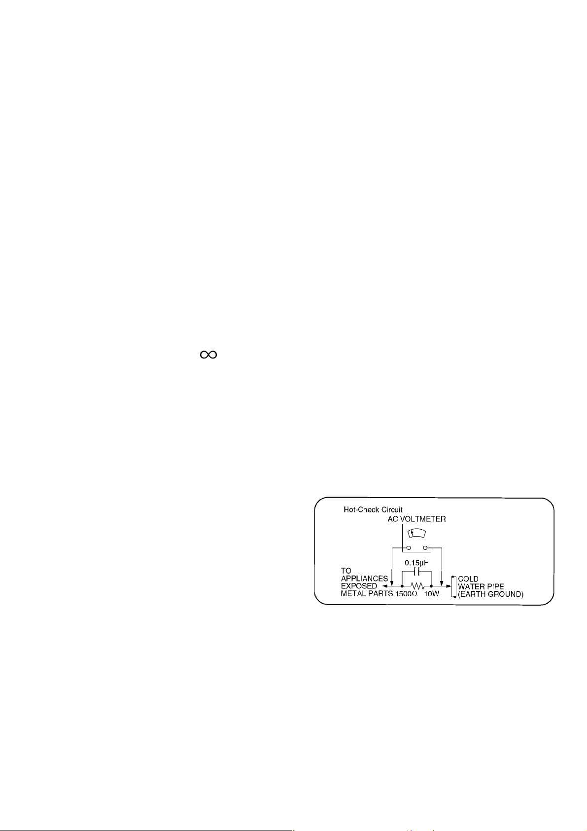
1.1.2. Leakage Current Hot Check (See Figure 1.)
1. Plug the AC cord directly into the AC outlet. Do not use
an isolation transformer for this check.
2. Connect a 1.5kohm, 10 watts resistor, in parallel with a
0.15μF capacitors, between each exposed metallic part
on the set and a good earth ground such as a water pipe,
as shown in Figure 1.
3. Use an AC voltmeter, with 1000 ohms/volt or more
sensitivity, to measure the potential across the resistor.
4. Check each exposed metallic part, and measure the
voltage at each point.
5. Reverse the AC plug in the AC outlet and repeat each of
the above measurements.
6. The potential at any point should not exceed 0.75 volts
RMS. A leakage current tester (Simpson Model 229 or
equivalent) may be used to make the hot checks, leakage
current must not exceed 1/2 milliamp. In case a
measurement is outside of the limits specified, there is a
possibility of a shock hazard, and the equipment should
be repaired and rechecked before it is returned to the
customer.
Figure 1
3
Page 4

TH-L32A20X
2Warning
2.1. Prevention of Electrostatic Discharge (ESD) to Electrostatically Sensitive (ES) Devices
Some semiconductor (solid state) devices can be damaged easily by static electricity. Such components commonly are called
Electrostatically Sensitive (ES) Devices. Examples of typical ES devices are integrated circuits and some field-effect transistors and
semiconductor [chip] components. The following techniques should be used to help reduce the incidence of component damage
caused by electrostatic discharge (ESD).
1. Immediately before handling any semiconductor component or semiconductor-equipped assembly, drain off any ESD on your
body by touching a known earth ground. Alternatively, obtain and wear a commercially available discharging ESD wrist strap,
which should be removed for potential shock reasons prior to applying power to the unit under test.
2. After removing an electrical assembly equipped with ES devices, place the assembly on a conductive surface such as
aluminum foil, to prevent electrostatic charge buildup or exposure of the assembly.
3. Use only a grounded-tip soldering iron to solder or unsolder ES devices.
4. Use only an anti-static solder removal device. Some solder removal devices not classified as [anti-static (ESD protected)] can
generate electrical charge sufficient to damage ES devices.
5. Do not use freon-propelled chemicals. These can generate electrical charges sufficient to damage ES devices.
6. Do not remove a replacement ES device from its protective package until immediately before you are ready to install it. (Most
replacement ES devices are packaged with leads electrically shorted together by conductive foam, aluminum foil or
comparable conductive material).
7. Immediately before removing the protective material from the leads of a replacement ES device, touch the protective material
to the chassis or circuit assembly into which the device will be installed.
Caution
Be sure no power is applied to the chassis or circuit, and observe all other safety precautions.
8. Minimize bodily motions when handling unpackaged replacement ES devices. (Otherwise ham less motion such as the
brushing together of your clothes fabric or the lifting of your foot from a carpeted floor can generate static electricity (ESD)
sufficient to damage an ES device).
4
Page 5
TH-L32A20X
2.2. About lead free solder (PbF)
Note: Lead is listed as (Pb) in the periodic table of elements.
In the information below, Pb will refer to Lead solder, and PbF will refer to Lead Free Solder.
The Lead Free Solder used in our manufacturing process and discussed below is (Sn+Ag+Cu).
That is Tin (Sn), Silver (Ag) and Copper (Cu) although other types are available.
This model uses Pb Free solder in it’s manufacture due to environmental conservation issues. For service and repair work, we’d
suggest the use of Pb free solder as well, although Pb solder may be used.
PCBs manufactured using lead free solder will have the PbF within a leaf Symbol PbF stamped on the back of PCB.
Caution
• Pb free solder has a higher melting point than standard solder. Typically the melting point is 50 ~ 70 °F (30~40 °C) higher. Please
use a high temperature soldering iron and set it to 700 ± 20 °F (370 ± 10 °C).
• Pb free solder will tend to splash when heated too high (about 1100 °F or 600 °C).
If you must use Pb solder, please completely remove all of the Pb free solder on the pins or solder area before applying Pb
solder. If this is not practical, be sure to heat the Pb free solder until it melts, before applying Pb solder.
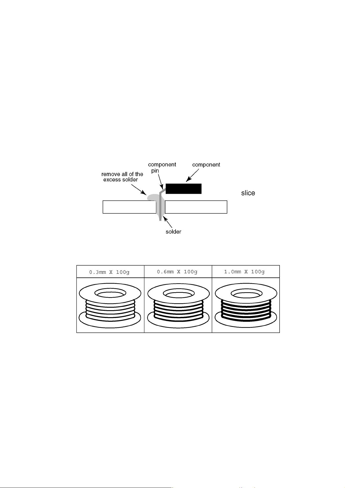
• After applying PbF solder to double layered boards, please check the component side for excess solder which may flow onto the
opposite side. (see figure below)
Suggested Pb free solder
There are several kinds of Pb free solder available for purchase. This product uses Sn+Ag+Cu (tin, silver, copper) solder.
However, Sn+Cu (tin, copper), Sn+Zn+Bi (tin, zinc, bismuth) solder can also be used.
5
Page 6
TH-L32A20X
3 Service Navigation
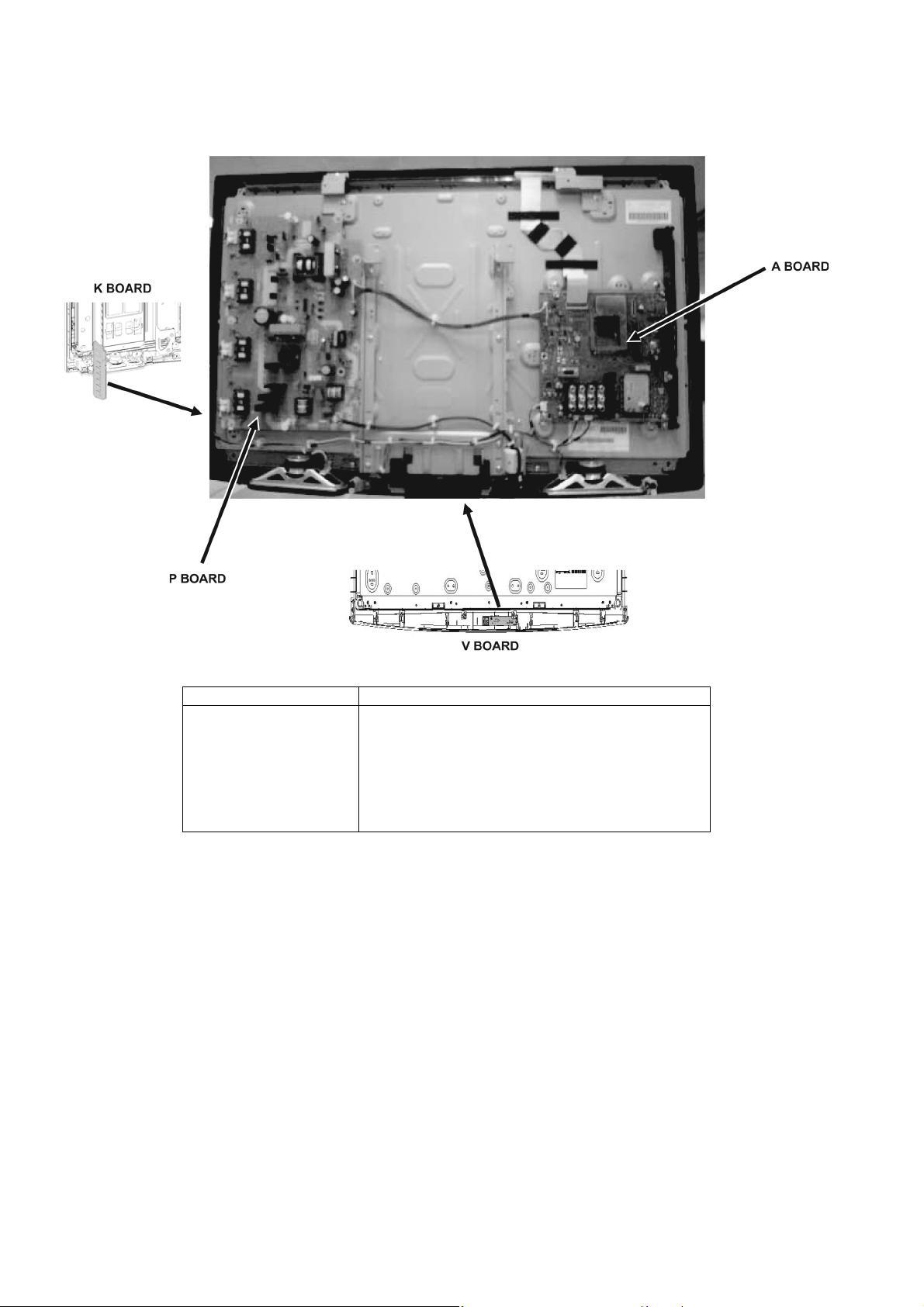
3.1. Service Hint
Board Name Function
A Board AVSW, TUN, GENX, PEAKS-AVCEEP, TEMP TUN
V Board REMOTE, LED, LUMINUNCE SENSOR
K Board CONTROL BUTTON, POWER BUTTON
P BOARD POWER AC / DC
6
Page 7
TH-L32A20X
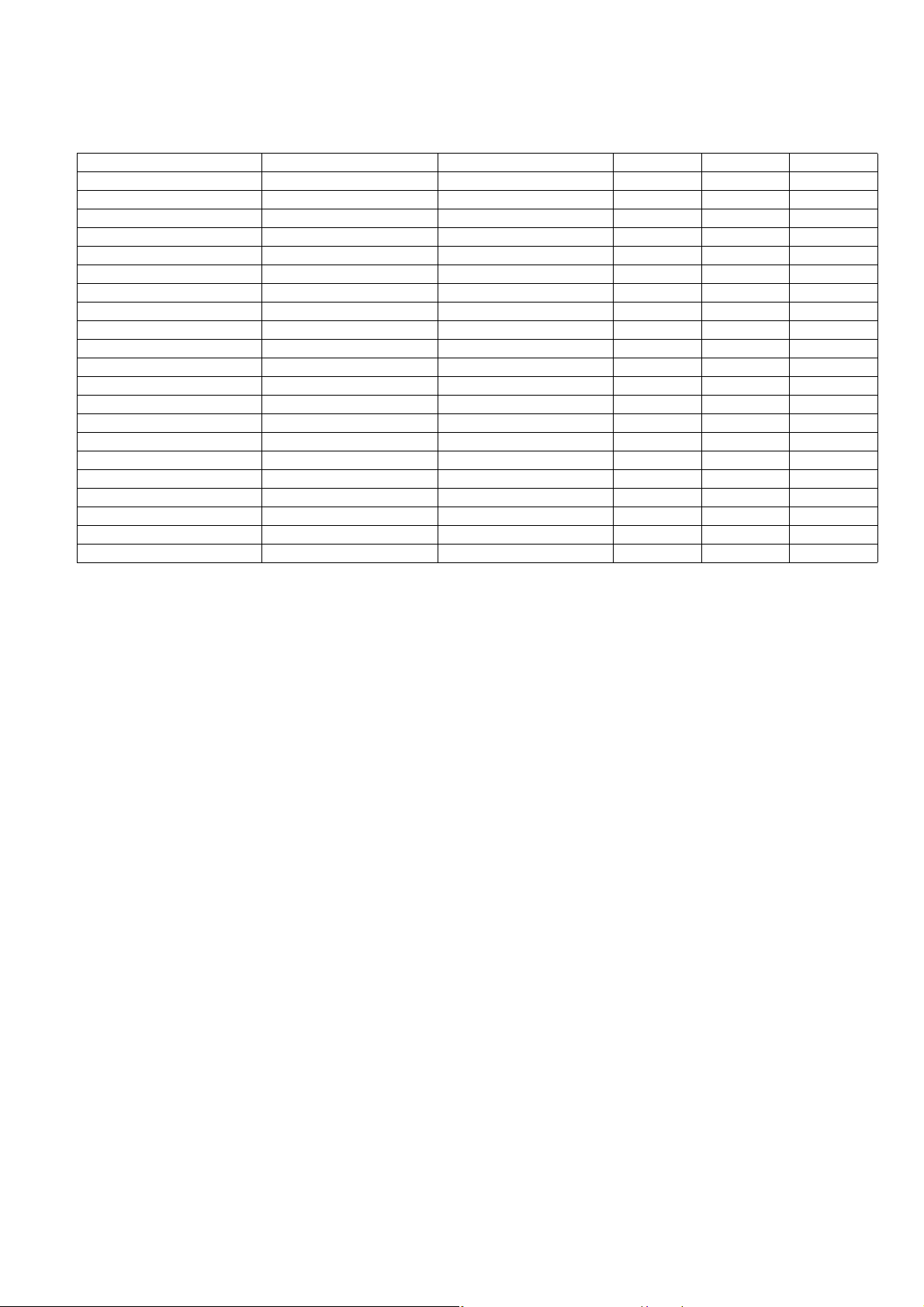
3.2. Applicable signals
Input signal that can be displayed
* Mark: Applicable input signal for Component (Y, P
horizontal frequency (kHz) vertical frequency (Hz) COMPONENT HDMI PC
525 (480) / 60i 15.73 59.94 * *
525 (480) /60p 31.47 59.94 * *
750 (720) /60p 45.00 59.94 * *
1,125 (1,080) /60i 33.75 59.94 * *
640 × 400 @70 31.47 70.08 *
640 × 480 @60 31.47 59.94 *
Macintosh13 inch (640 × 480) 35.00 66.67 *
640 × 480 @75 37.50 75.00 *
852 × 480 @60 31.47 59.94 *
800 × 600 @60 37.88 60.32 *
800 × 600 @75 46.88 75.00 *
800 × 600 @85 53.67 85.08 *
Macintosh16 inch (832 × 624) 49.73 74.55 *
1,024 × 768 @60 48.36 60.00 *
1,024 × 768 @70 56.48 70.07 *
1,024 × 768 @75 60.02 75.03 *
1,024 × 768 @85 68.68 85.00 *
Macintosh 21 inch (1,152 × 870) 68.68 75.06 *
1,280 × 768 @60 47.70 60.00 *
1,280 × 1,024 @60 63.98 60.02 *
1,366 × 768 @60 48.36 60.00 *
Note:
• Signals other than above may not be displayed properly.
• The above signals are reformatted for optimal viewing on your display.
, PR), HDMI and PC
B
7
Page 8

TH-L32A20X
4 Specifications
Power Source AC AUTO 110 - 240 V, 50 / 60 Hz
Power Consumption
Average use 94 W
Standby Condition 0.3 W
Display panel
Aspect Ratio 16:9
Visible screen size 80 cm (diagonal)
698 mm (W) × 393 mm (H)
Number of pixels 1,049,088 (1,366 (W) × 768 (H))
Sound
Speaker WOOFER × 2 pcs, 8 Ω
MID RANGE × 2 pcs, 8 Ω
Audio Output WOOFER : 20 W (10 W + 10 W), 10% THD
Headphones M3 (3.5 mm) stereo mini Jack × 1
PC signals VGA, SVGA, WVGA, XGA
Receiving Systems / Band name 17 SYSTEMS FUNCTIONS
Receiving Channels (Regular TV)
PAL B/ G 2 - 12 (PAL / SECAM B, K1)
UHF BAND 21 - 69 (PAL G, H, I / SECAM G, K, K1)
28 - 69 (PAL B AUST.)
13 - 57 (PAL D, K)
13 - 62 (NTSC M JAPAN)
14 - 69 (NTSC M USA)
CATV S1 - S20 (OSCAR)
1 - 125 (USA CATV)
C13 - C49 (JAPAN)
S21 - S41 (HYPER)
Z1 - Z37 (CHINA)
Aerial - Rear VHF / UHF
Operating Conditions
Connection Terminals
AV1 Input AUDIO L-R RCA PIN Type × 2 0.5 V [rms]
VIDEO RCA PIN Type × 1 1.0 V [p-p] (75 Ω)
COMPONENT Y 1.0 V [p-p] (including synchronization)
AV2 Input AUDIO L-R RCA PIN Type × 2 0.5 V [rms]
VIDEO RCA PIN Type × 1 1.0 V [p-p] (75 Ω)
MID RANGE : 10 W (5 W + 5 W), 10% THD
SXGA, WXGA ...... (compressed)
Horizontal scanning frequency 31 - 69 kHz
Vertical scanning frequency 59 - 86 Hz
1 PAL B, G, H
2 PAL I
3 PAL D, K
4 SECAM B, G
5 SECAM D, K
6 SECAM K1
7 NTSC M (NTSC 3.58 / 4.5MHZ)
8 NTSC 4.43 / 5.5 MHz
9 NTSC 4.43 / 6.0 MHz
10 NTSC 4.43 / 6.5 MHz
11 NTSC 3.58 / 5.5 MHz
12 NTSC 3.58 / 6.0 MHz
13 NTSC 3.58 / 6.5 MHz
14 SECAM I
15 PAL 60 Hz / 5.5 MHz Playback from Special Disc Players and
16 PAL 60 Hz / 6.0 MHz
17 PAL 60 Hz / 6.5 MHz
0 - 12 (PAL B AUST.)
1 - 9 (PAL B N.Z.)
1 - 12 (PAL / SECAM D)
1 - 12 (NTSC M JAPAN)
2 - 13 (NTSC M USA)
5A, 9A (AUST.)
Temperature : 0°C - 40°C
Humidity : 20 % - 80 % RH (non-condensing)
, PR/C
P
B/CB
R
Reception of broadcast transmission and
playback from video cassette tape recorders.
Playback from special VCR’s or DVD.
Special VCR’s or DVD.
± 0.35 V [p-p]
8
Page 9

AV3 Input AUDIO L-R RCA PIN Type × 2 0.5 V [rms]
VIDEO RCA PIN Type × 1 1.0 V [p-p] (75 Ω)
Monitor Output AUDIO L-R RCA PIN Type × 2 0.5 V [rms] (high impedance)
VIDEO RCA PIN Type × 1 1.0 V [p-p] (75 Ω)
Others HDMI 1 - 3 Input TYPE A Connectors • This TV supports “HDAVI Control 5” function.
PC Input HIGH-DENSITY D-SUB 15 PIN R, G, B / 0.7 V[p-p] (75 Ω)
HD, VD / TTL LEVEL 2.0-5.0 V [p-p] (high impedance)
Card Slot SD Card slot × 1
Dimension (W x H x D) 855 mm × 553 mm × 217 mm (With Pedestal)
855 mm × 513 mm × 120 mm (TV only)
Mass 12.0 kg Net (With Pedestal)
10.0 kg Net (TV only)
Note
Design and Specifications are subject to change without notice. Mass and Dimensions shown are approximate.
TH-L32A20X
9
Page 10
TH-L32A20X
5 Service Mode
5.1. How to enter into Service Mode
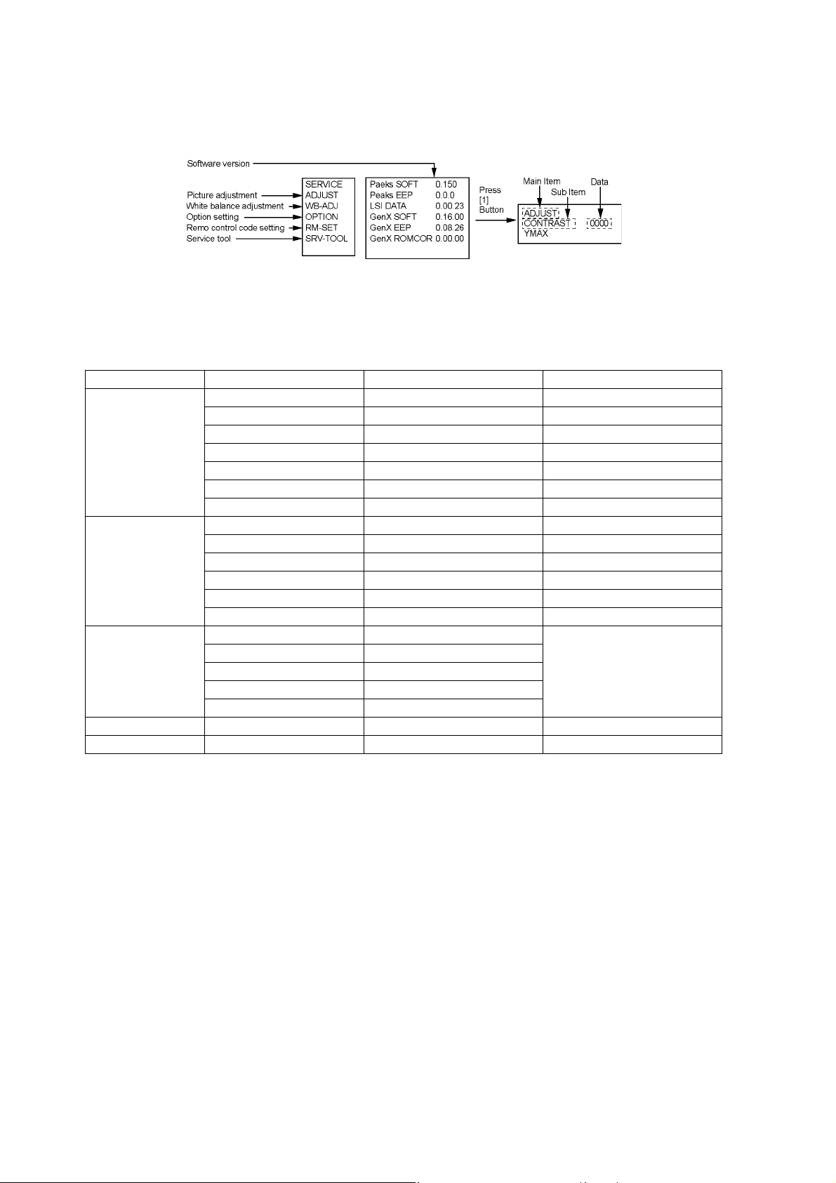
While pressing [VOLUME ( - )] button of the main unit, press [INFO] button of the remote control three times within 2 seconds.
5.1.1.
• Value is shown as a hexadecimal number.
• Preset value differs depending on models.
• After entering the adjustment mode, take note of the value in each item before starting adjustment.
Contents of adjustment mode
Main item Sub item Sample Data Remark
ADJUST CONTRAST 000
COLOR 4C
TINT 00
SUB-BRT 808
BACKLGT 22E
B-Y-G 34
R-Y-A 00
WB-ADJ R-GAIN F7
G-GAIN FB
B-GAIN DB
R-CENT 82
G-CENT 80
B-CENT 86
OPTION Boot ROM Factory Preset.
STBY-SET 00
EMERGENCY ON
CLK MODE 00
CLOCK 0E4
RM-SET 00 Fixed.
SRV-TOOL 00 See next.
5.1.2. How to exit
Switch off the power with the [POWER] button on the main unit or the [POWER] button on the remote control.
10
Page 11
TH-L32A20X
5.2. SRV-TOOL
5.2.1. How to access
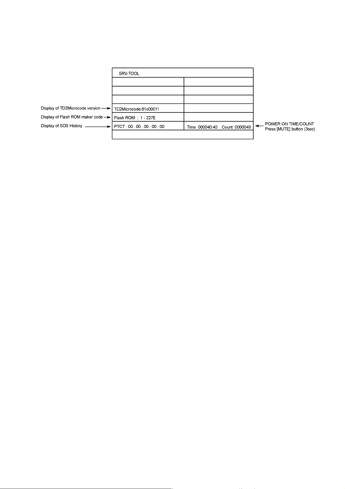
1. Select [SRV-TOOL] in Service Mode.
2. Press [OK] button on the remote control.
5.2.2. Display of SOS History
SOS History (Number of LED blinking ) indication.
From left side; Last SOS, before Last, three occurrence before, 2nd occurrence after shipment, 1st occurrence after shipment.
This indication except 2nd and 1st occurrence after shipment will be cleared by [Self-check indication and forced to factory
shipment setting].
5.2.3. POWER ON TIME/COUNT
Note : To display TIME/COUNT menu, highlight position, then press MUTE for 3sec.
Time : Cumulative power on time, indicated hour : minute by decimal
Count : Number of ON times by decimal
Note : This indication will not be cleared by either of the self-checks or any other command.
5.2.4. Exit
1. Disconnect the AC cord from wall outlet.
11
Page 12
TH-L32A20X
5.3. Service Mode Adjustment
1. Press the “RECALL” button on the remote control and press “ -” vol button on the LCD panel.
2. Press button number 1 on the remote control to select for Adjustment.
3. Self Check to Exit.
5.3.1. Self Check Mode
1. Press the “MENU” button (on the remote control) and the “DOWN” button on the LCD panel.
2. Press ON/OFF button on the panel to Exit.
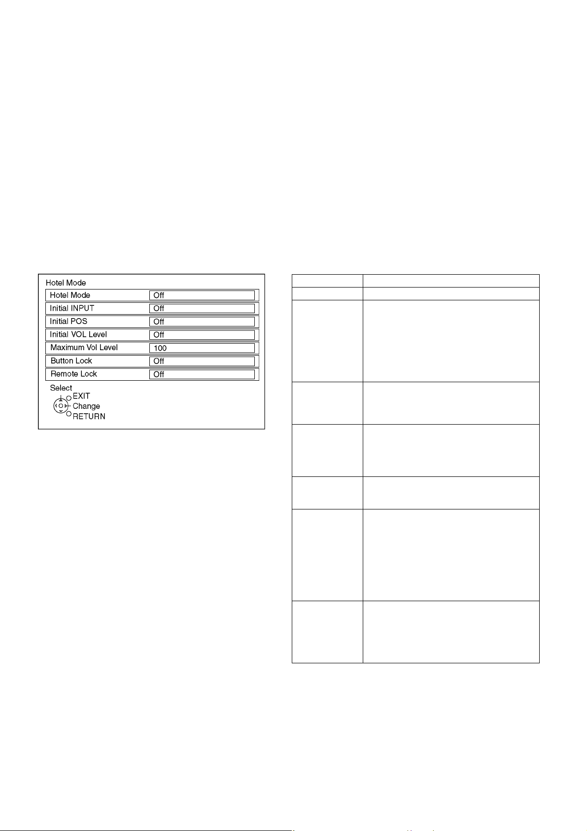
5.3.2. Hotel Mode Adjustment
1. Press the “VOLUME DOWN” button on the TV panel and simultaneously press the AV button on the remote control 3 times to
enter Hotel Mode.
2. Set Hotel mode “on”, then press “EXIT” to come out.
5.3.3. Hotel Mode
Item Function
Hotel Mode Select hotel mode ON/OFF
Initial INPUT Select input signal modes.
Initial POS Select programme number.
Initial VOL level Adjust the volume when each time power is
Maximum VOL
level
Button lock Select local key conditions.
Remote lock Select remote control key conditions.
Set the input, when each time power is switched
on.
Selection :
OFF/Analogue TV/Digital TV/AV1/AV2/AV3/PC/
HDMI1/HDMI2/HDMI3
• Off: give priority to a last memory.
• Selectable input is depend on the model.
Selection :
Off/0 to 100
• Off: give priority to a last memory.
switched on.
Selection/Range :
Off/0 to 100
• Off: give priority to a last memory.
Adjust maximum volume.
Range :
0 to 100
Selection :
Off/SETUP/MENU/All
• Off: altogether valid.
• SETUP: only F-key is invalid.
(Tuning guide (menu) can not be selected.)
• MENU: only F-key is invalid.
(only Volume/Mute can be selected.)
• ALL: altogether invalid.
Selection :
Off/SETUP/MENU
• Off: altogether valid.
• SETUP: only Setup menu is invalid.
• MENU: Picture/Sound/Setup menu are invalid.
12
Page 13
TH-L32A20X
6 Troubleshooting Guide
Use the self-check function to test the unit.
1. Checking the IIC bus lines
2. Power LED Blinking timing
6.1. Check of the IIC bus lines
6.1.1. How to access
Self-check indication only:
Produce TV reception screen, and while pressing [VOLUME ( - )] button on the main unit, press [OK] button on the remote control
for more than 3 seconds.
Self-check indication and forced to factory shipment setting:
Produce TV reception screen, and while pressing [VOLUME ( - )] button on the main unit, press [MENU] button on the remote
control for more than 3 seconds.
6.1.2. Exit
Disconnect the AC cord from wall outlet.
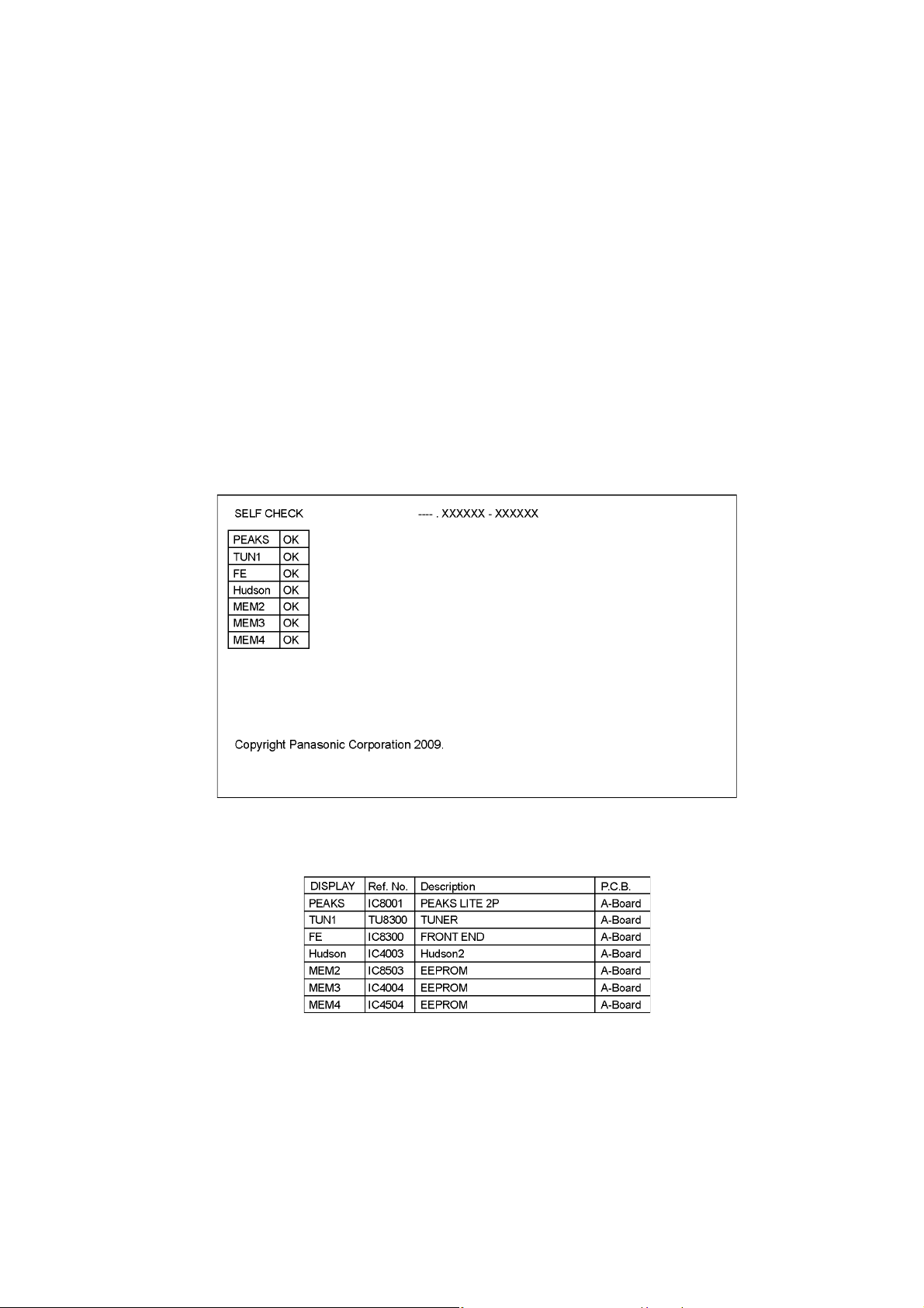
6.1.3. Screen display
6.1.4. Check Point
Confirm the following parts if NG was displayed.
13
Page 14
TH-L32A20X
6.2. Power LED Blinking timing chart
1. Subject
Information of LED Flashing timing chart.
2. Contents
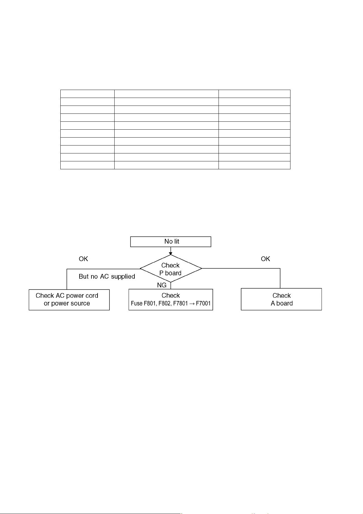
When an abnormality occurs, the protection circuit will operate and reset the unit to stand by mode. During this time, the
defective block can be identified by the number of blinking times of the Power LED on the front panel of the unit as follow:
Blinking times Contents BOARD
1 Inverter_SOS P BOARD
2 SUB 1.8V_SOS A BOARD
3 SUB 1.2V_SOS A BOARD
4 POWER_SOS P/A BOARD
5 SUB 5V_SOS A BOARD
9 TCON_SOS A BOARD
10 SUB 3.3V_SENSE A BOARD
11 DCDC_SOS A BOARD
12 SOS A BOARD
6.3. No Power
First check point
There are following 2 states of No Power indication by power LED.
1. No lit
2. Red is lit then turns red blinking a few seconds later. (See 6.2.)
14
Page 15
7 Disassembly and Assembly Instructions
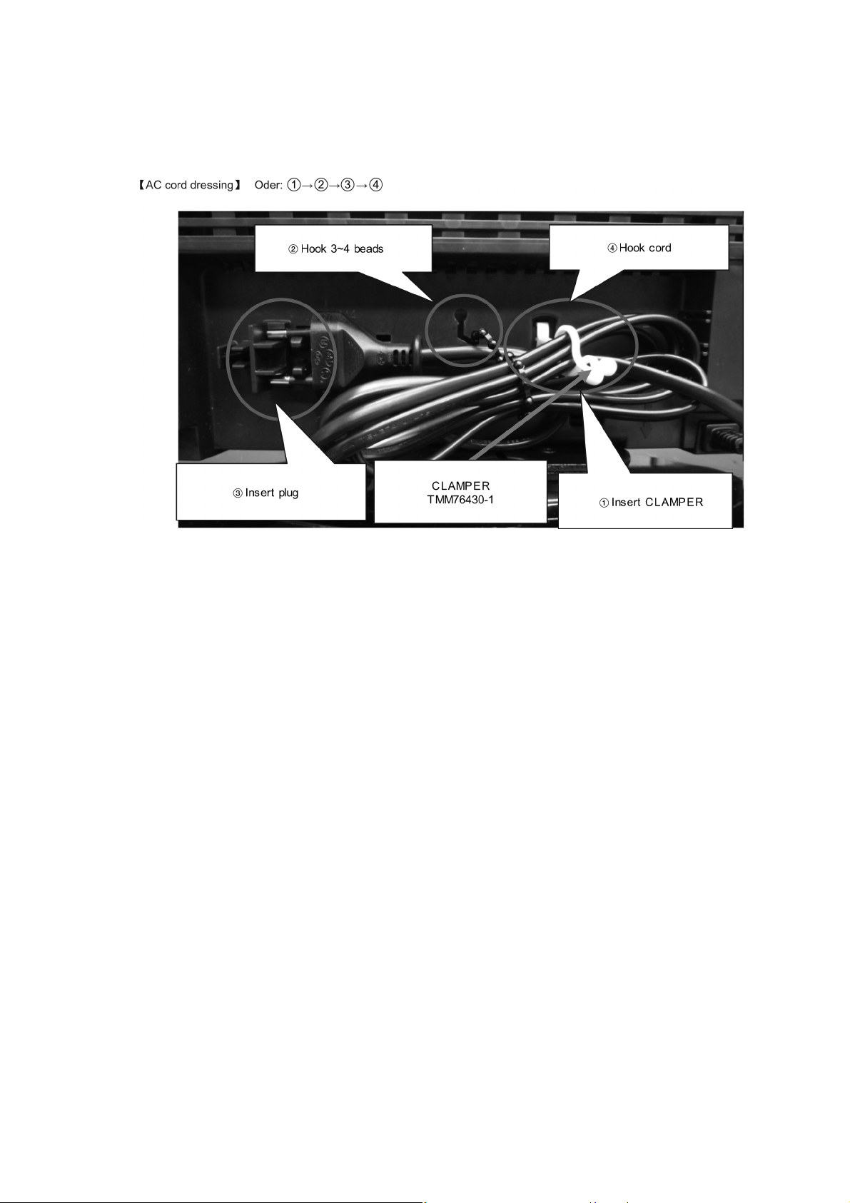
7.1. AC Cord Dressing
TREATMENT AC CORD.
TH-L32A20X
15
Page 16
TH-L32A20X
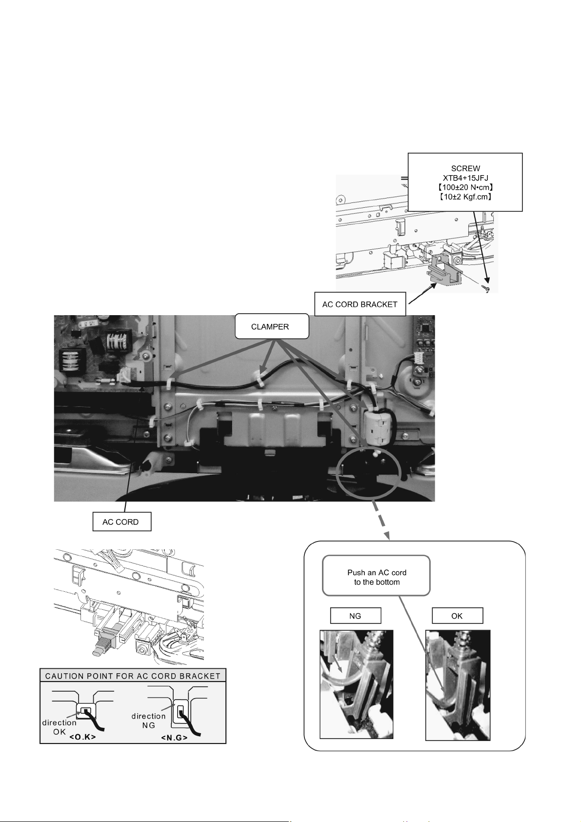
7.2. AC Cord Installation
1. Put on the AC CORD BRACKET on the CABINET.
2. Fix the AC CORD BRACKET with SCREW.
3. Insert AC CORD connector into P-PCB connector.
4. Clamp the AC CORD.
5. Insert AC CORD bushing into the AC CORD BRACKET.
6. AC code is pushed into the bottom of the bracket.
16
Page 17
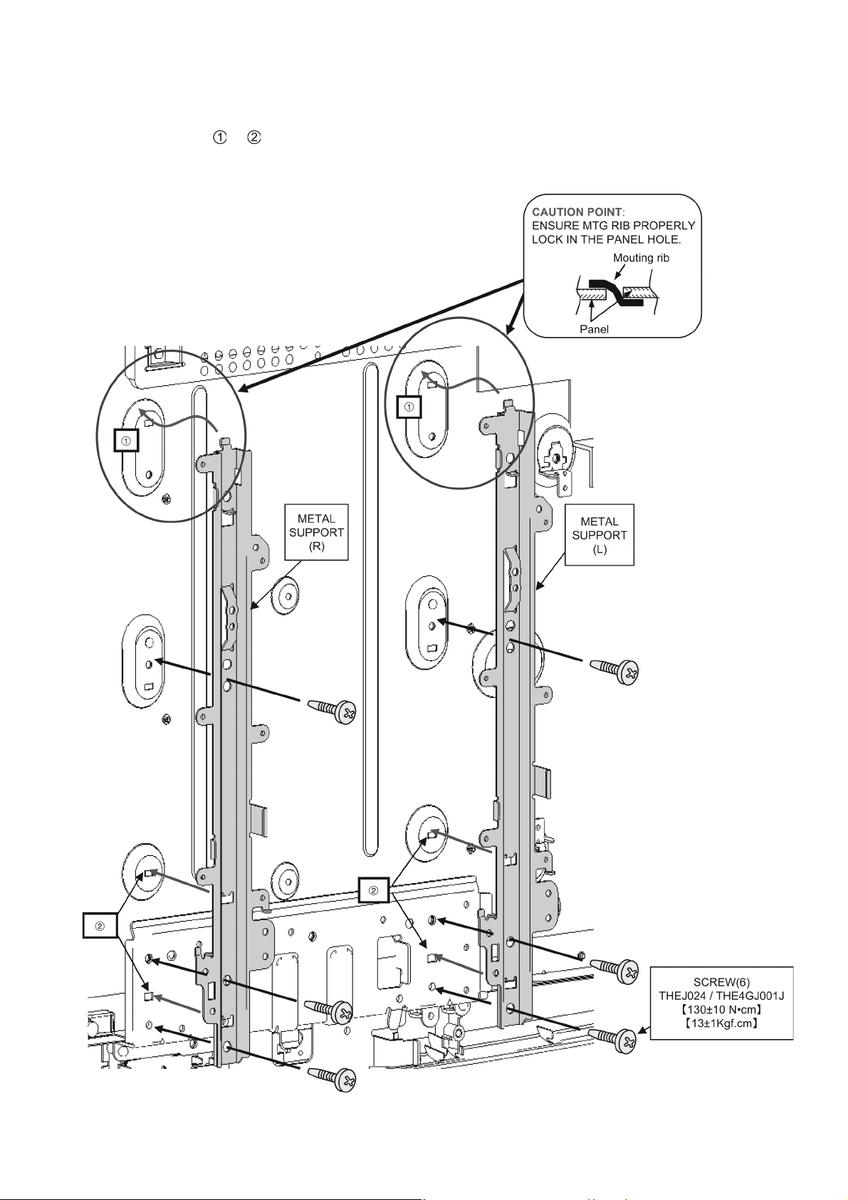
7.3. VESA Rail Installation
1. Stick the FELT.
2. Metal Support on the LCD PANEL.
(insert positioning.
3. Fix them with SCREW.
→
)
TH-L32A20X
17
Page 18
TH-L32A20X
7.4. VESA Metal Assembly
1. Put VESA METAL TOP AT L & R on the METAL SUPPOUT.
2. Fix them with SCREW.
18
Page 19
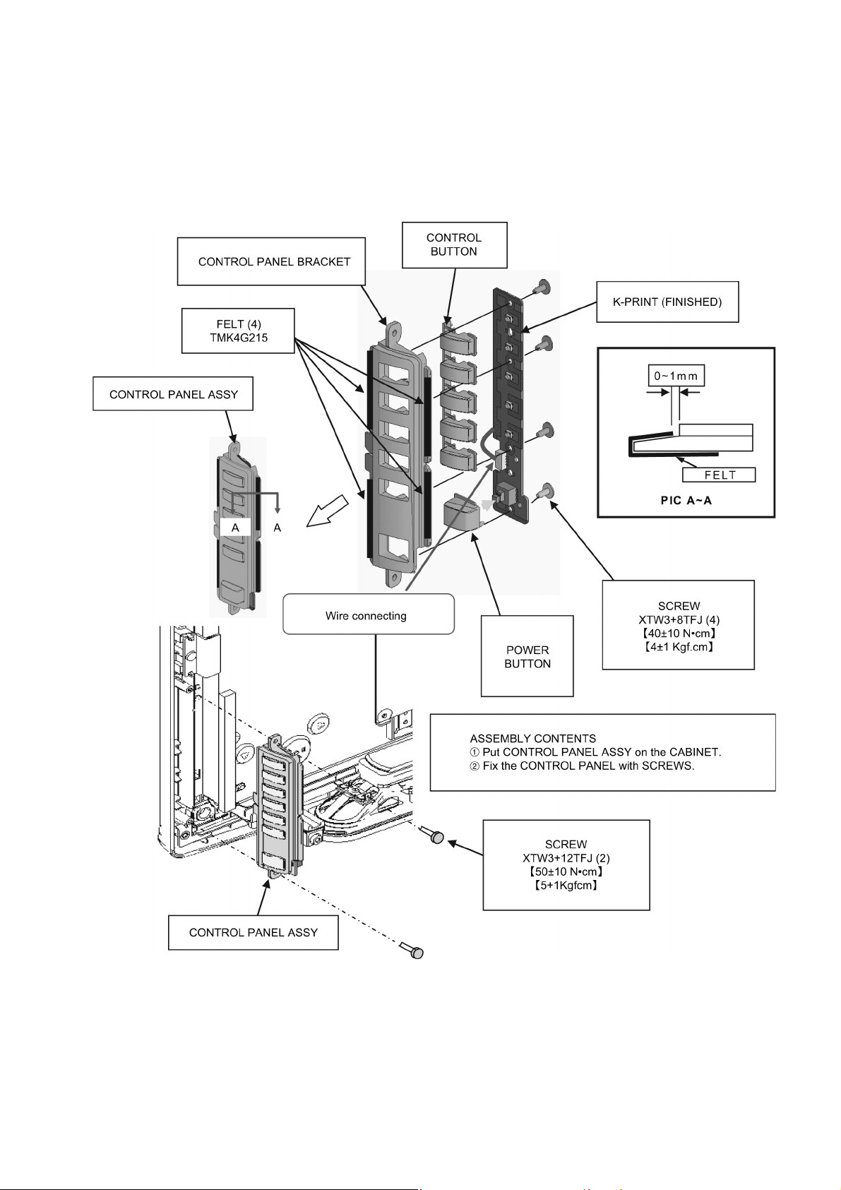
7.5. Control Panel Assembly
1. Stick the FELT to CONTROL BUTTON.
2. Wire connecting. (K1)
3. Assemble POWER BUTTON to the K-PRINT.
4. Assemble K-PRINT, CONTROL BUTTON, CONTROL PANEL BRACKET.
5. Fix them with SCREWS.
6. Stick the FELT to CONTROL PANEL BRACKET.
TH-L32A20X
19
Page 20
TH-L32A20X
7.6. Side AV Bracket Assembly
1. Put SIDE AV BRACKET ASSY ON LCD PANEL.
2. Fix them with screw.
20
Page 21
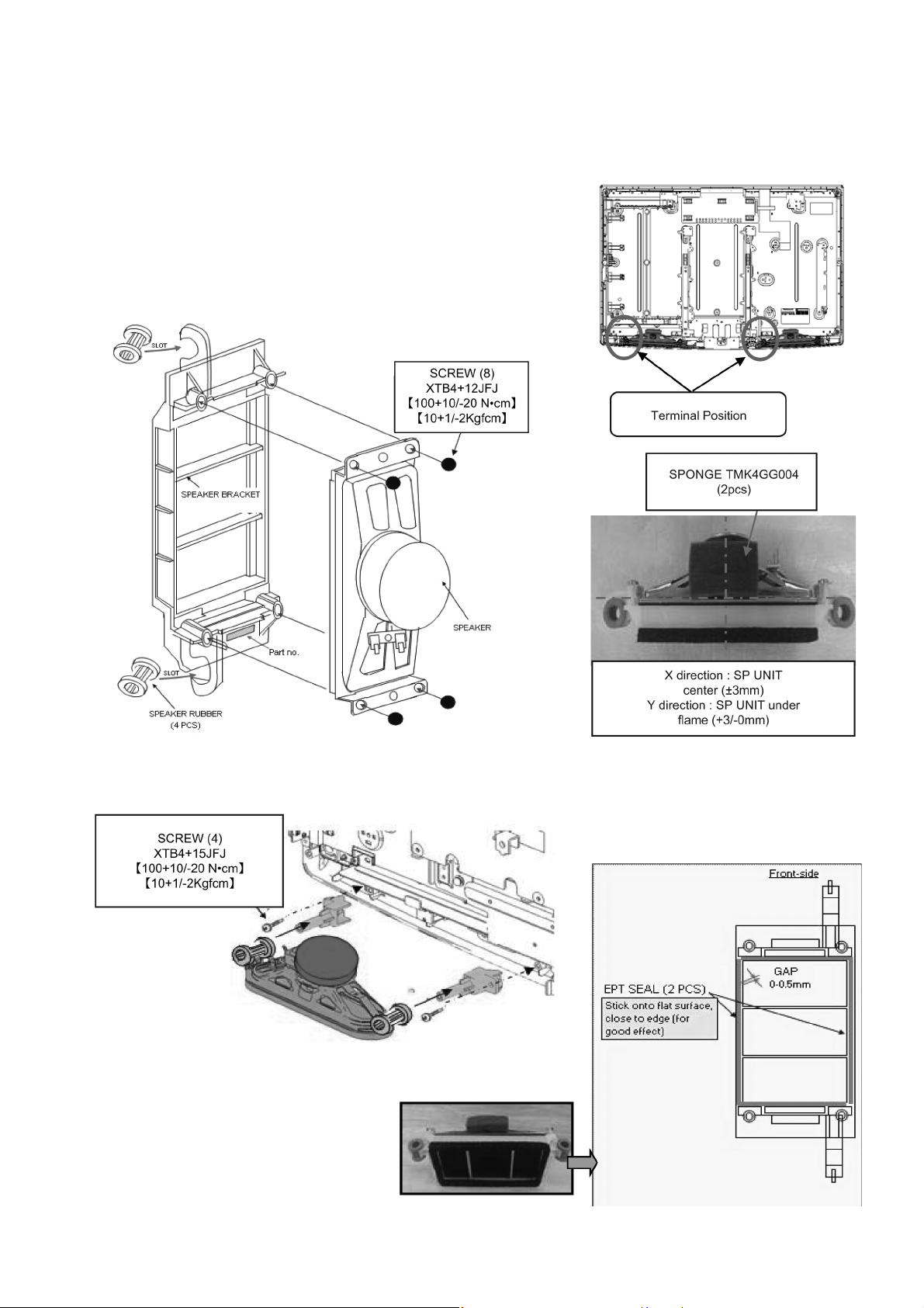
7.7. SP Installation
1. Fix SP RUBBER BUSH on SP UNIT.
2. Fix SP UNIT on the SP Bracket.
3. Fix them with SCREW.
4. Stick EPT SEAL on SP Bracket.
TH-L32A20X
21
Page 22
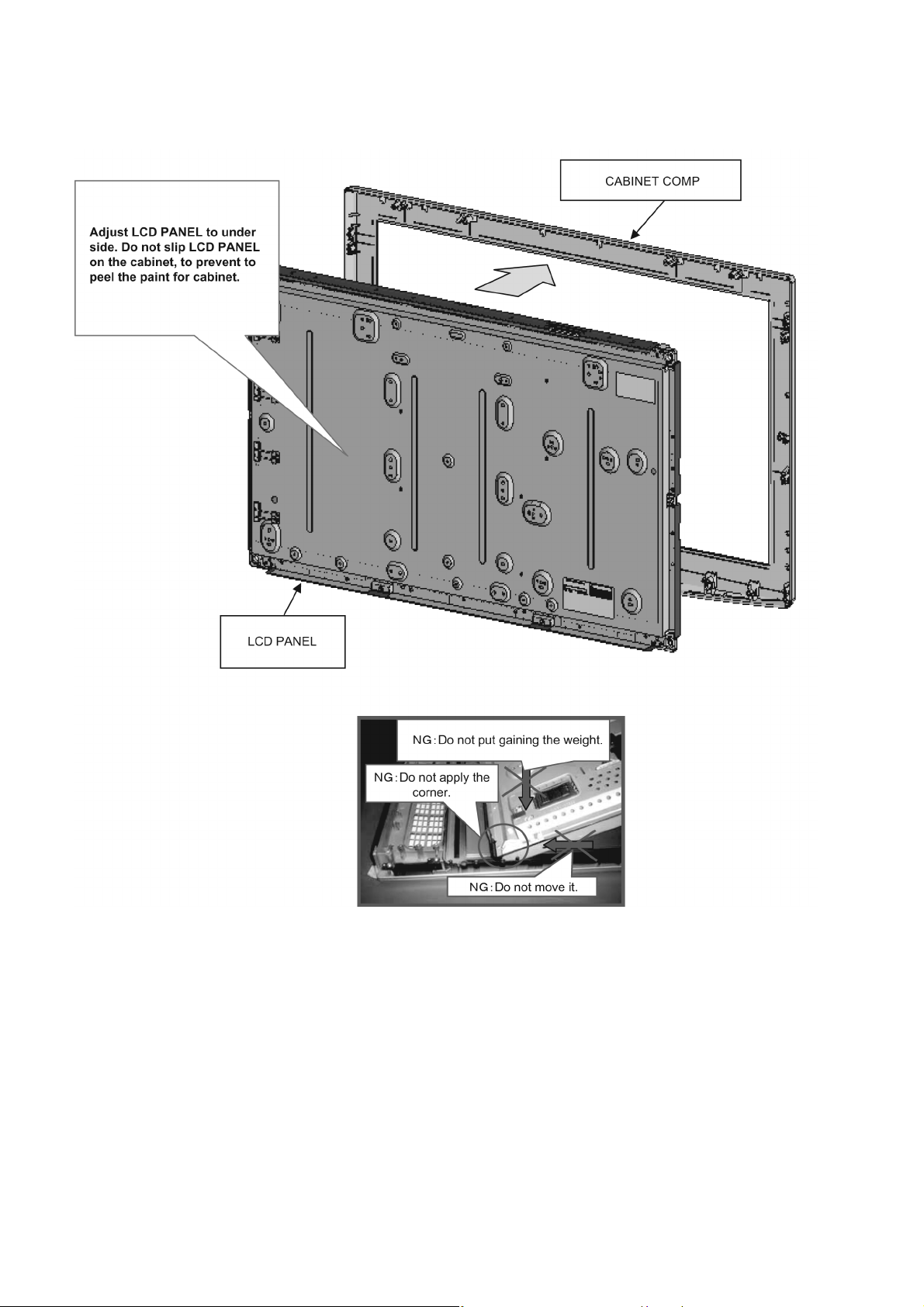
TH-L32A20X
7.8. LCD Panel Installation
Put LCD PANEL on the CABINET.
22
Page 23
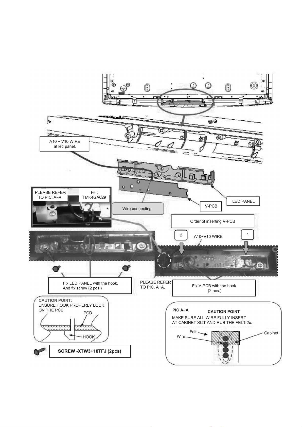
7.9. LED Panel Installation & Fitting
1. Fix LED PANEL on CABINET.
2. Wire connecting wire make sure fully insert at cabinet slit (V10).
3. Put V-PCB on CABINET.
4. Fix them with SCREW.
TH-L32A20X
23
Page 24
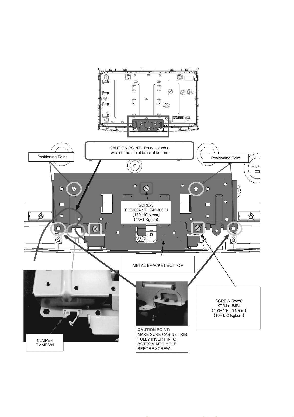
TH-L32A20X
7.10. LCD Mounting Installation 1
1. Put clamper on METAL BRACKET BOTTOM.
2. Put METAL BRACKET BOTTOM on the LCD PANEL.
3. Fix them with screw.
4. Wire dressing and lock CLAMPER.
24
Page 25
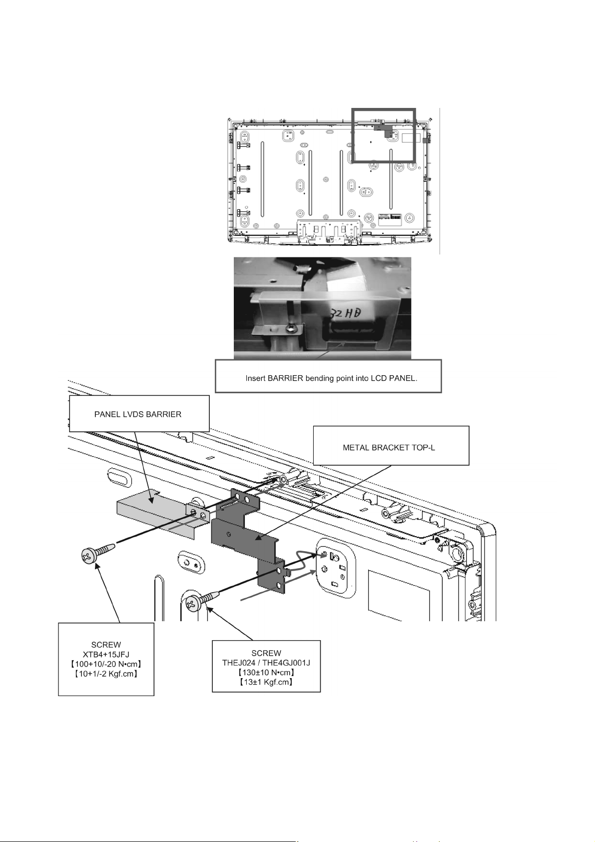
7.11. LCD Mounting Installation 2
1. Put BARRIER & METAL BRACKET TOP-L on the LCD PANEL.
2. Fix them with screw.
TH-L32A20X
25
Page 26
TH-L32A20X
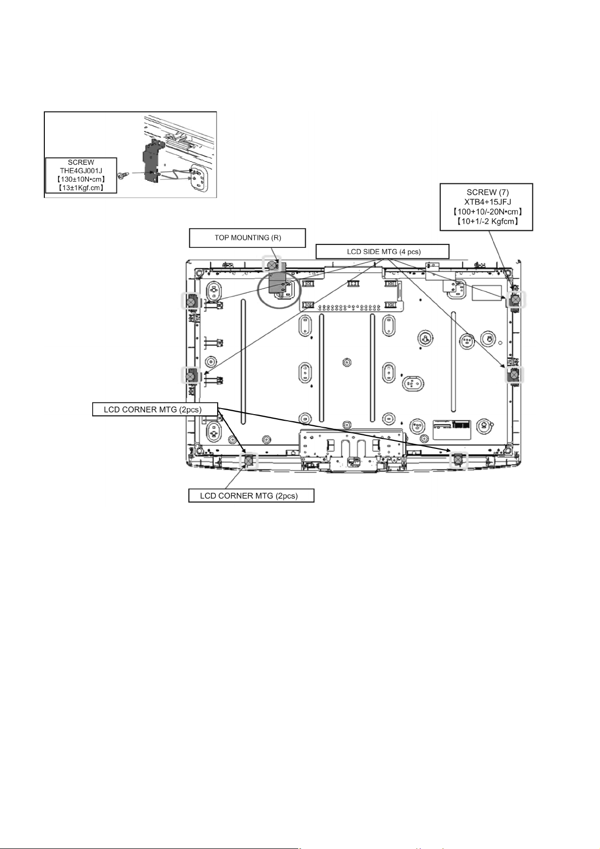
7.12. LCD Mounting Installation 3
1. Put LCD CORNER MTG/LCD-SIDE MTG & TOP MOUNTING ® ON THE LCD PANEL.
2. Fix them with screw.
26
Page 27
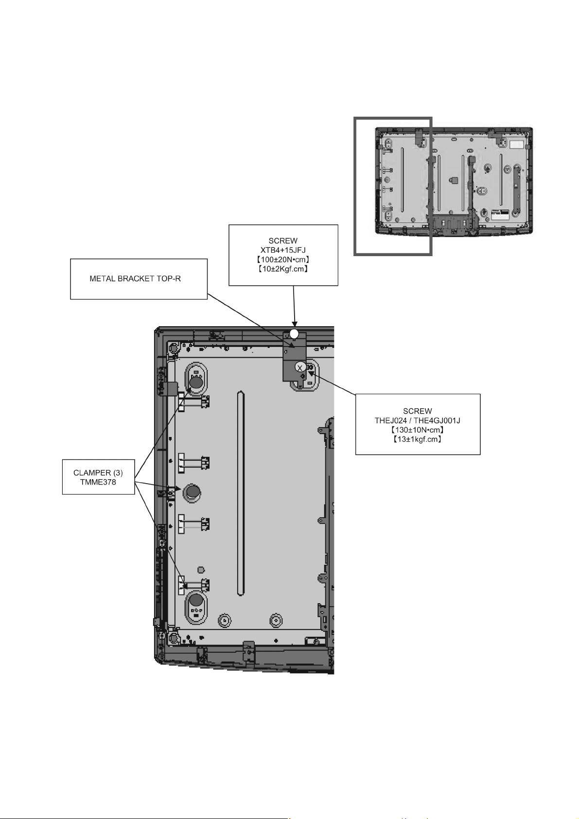
7.13. Metal Bracket Installation
1. Put Metal Bracket Top R on the LCD PANEL.
2. Fix them with SCREW.
3. Insert the CLAMPER.
TH-L32A20X
27
Page 28
TH-L32A20X
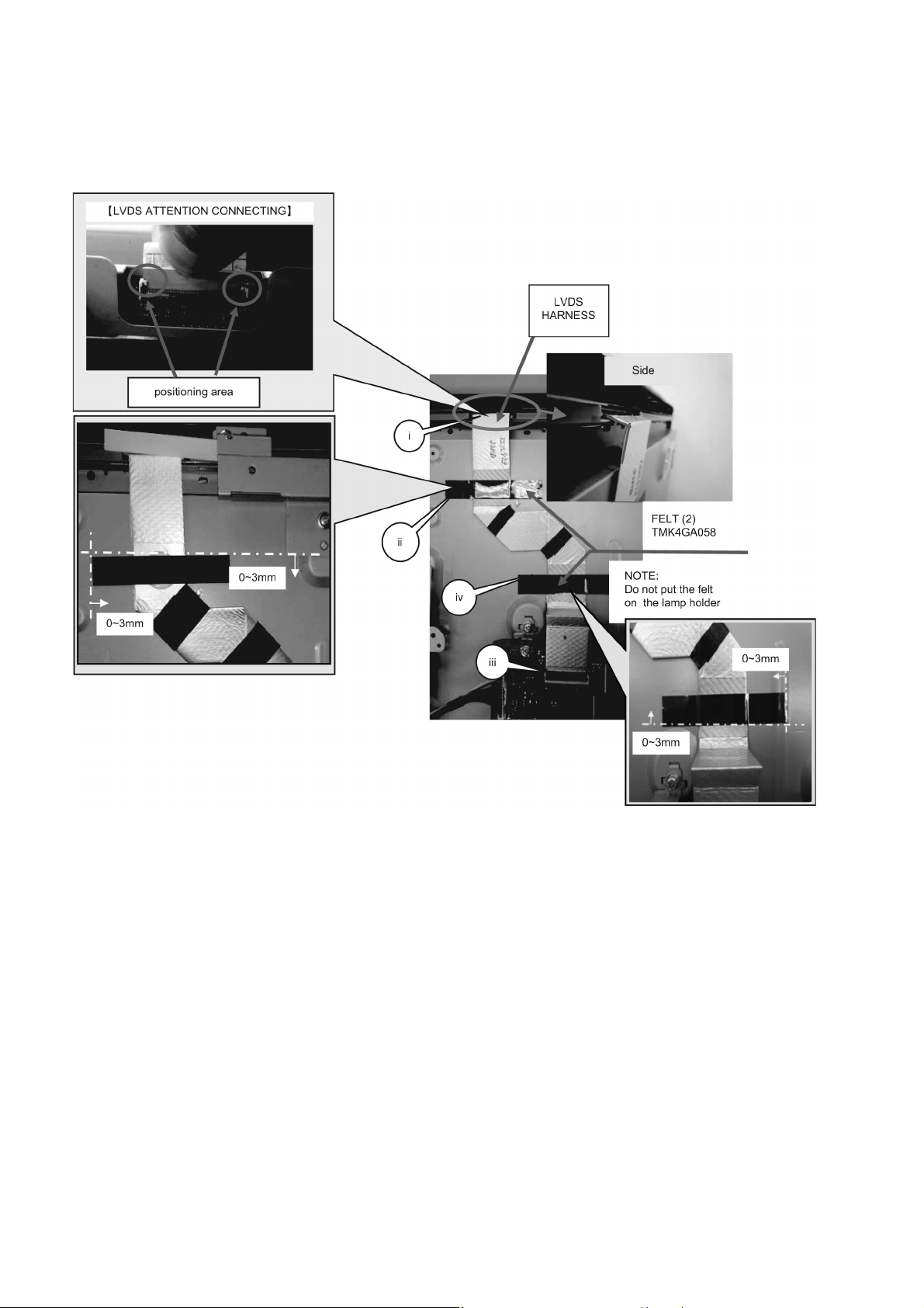
7.14. LVDS Installation
1. Put LVDS HARNESS to LCD PANEL with FELT.
→
ii → iii → iv.
i
2. Put PET/AL-TAPE on LCD PANEL.
28
Page 29
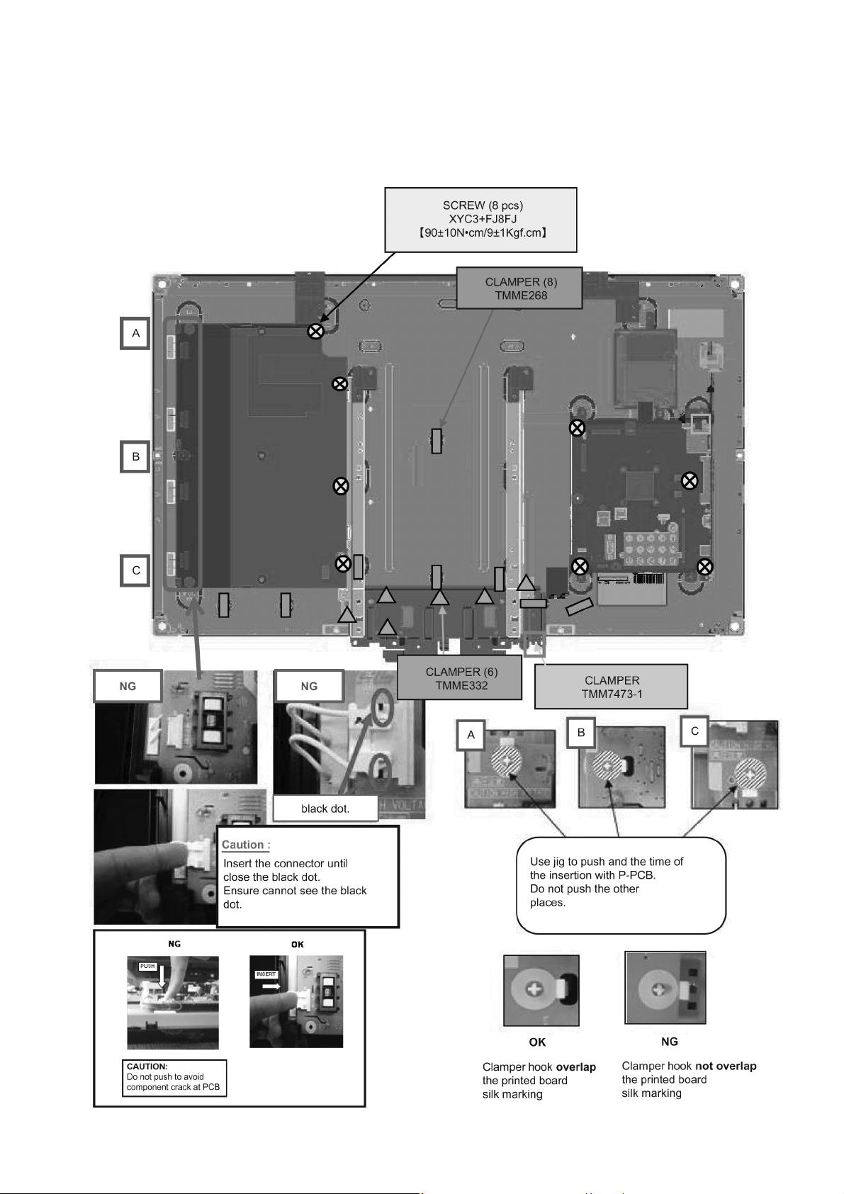
7.15. PCB and Clamper Assembly
1. Put the P-PCB, A-PCB on the MTG METAL.
2. Fix them with SCREWS.
3. Setting the CLAMPER.
4. Insert inv-lead in P PCB.
TH-L32A20X
29
Page 30
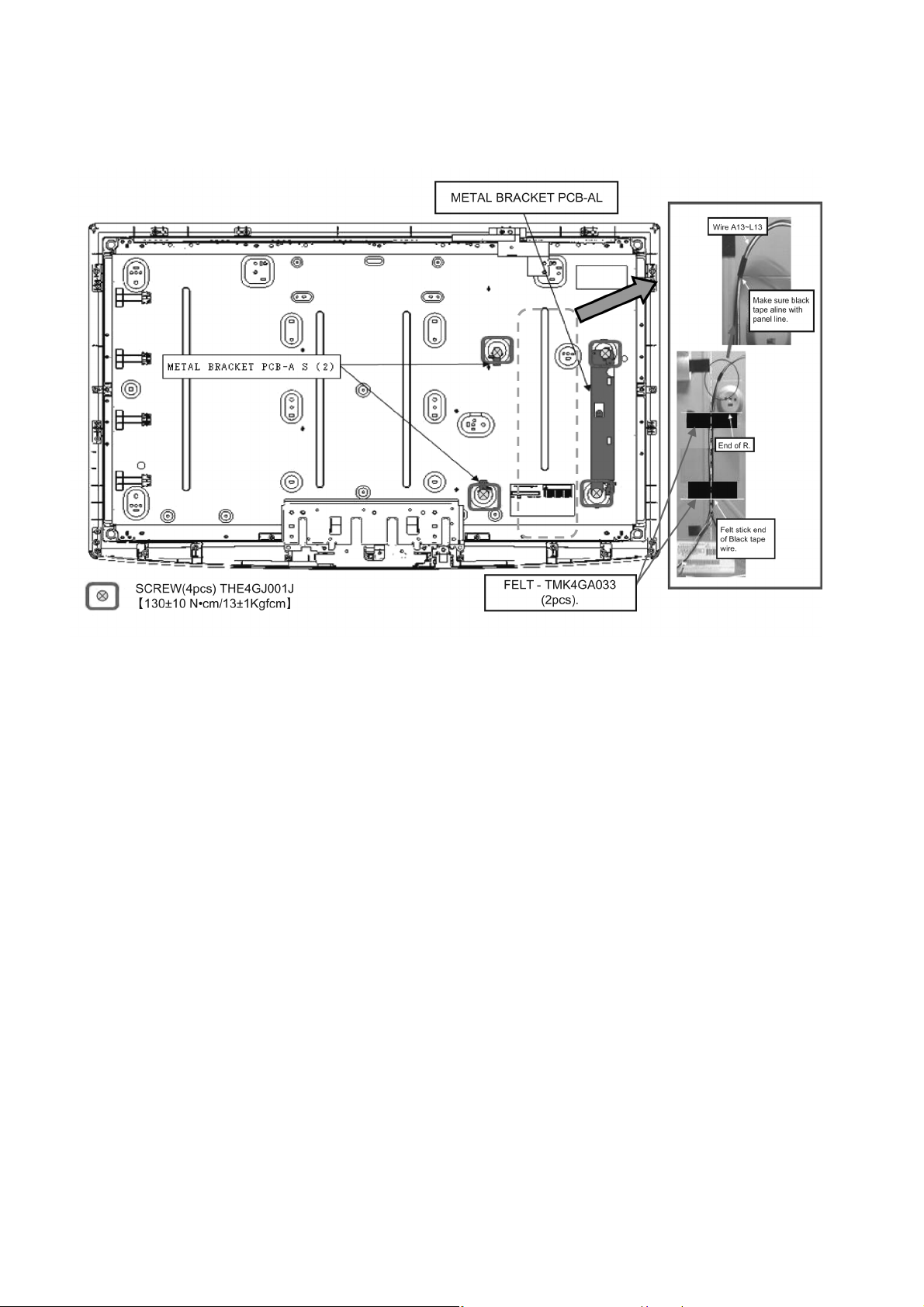
TH-L32A20X
7.16. PB MTG Installation
1. Put METAL BRACKET PCB-AS/AL on the LCD PANEL.
2. Fix them with SCREW. Add wire A13~L13 and fix 2 pcs felt follow the picture.
30
Page 31
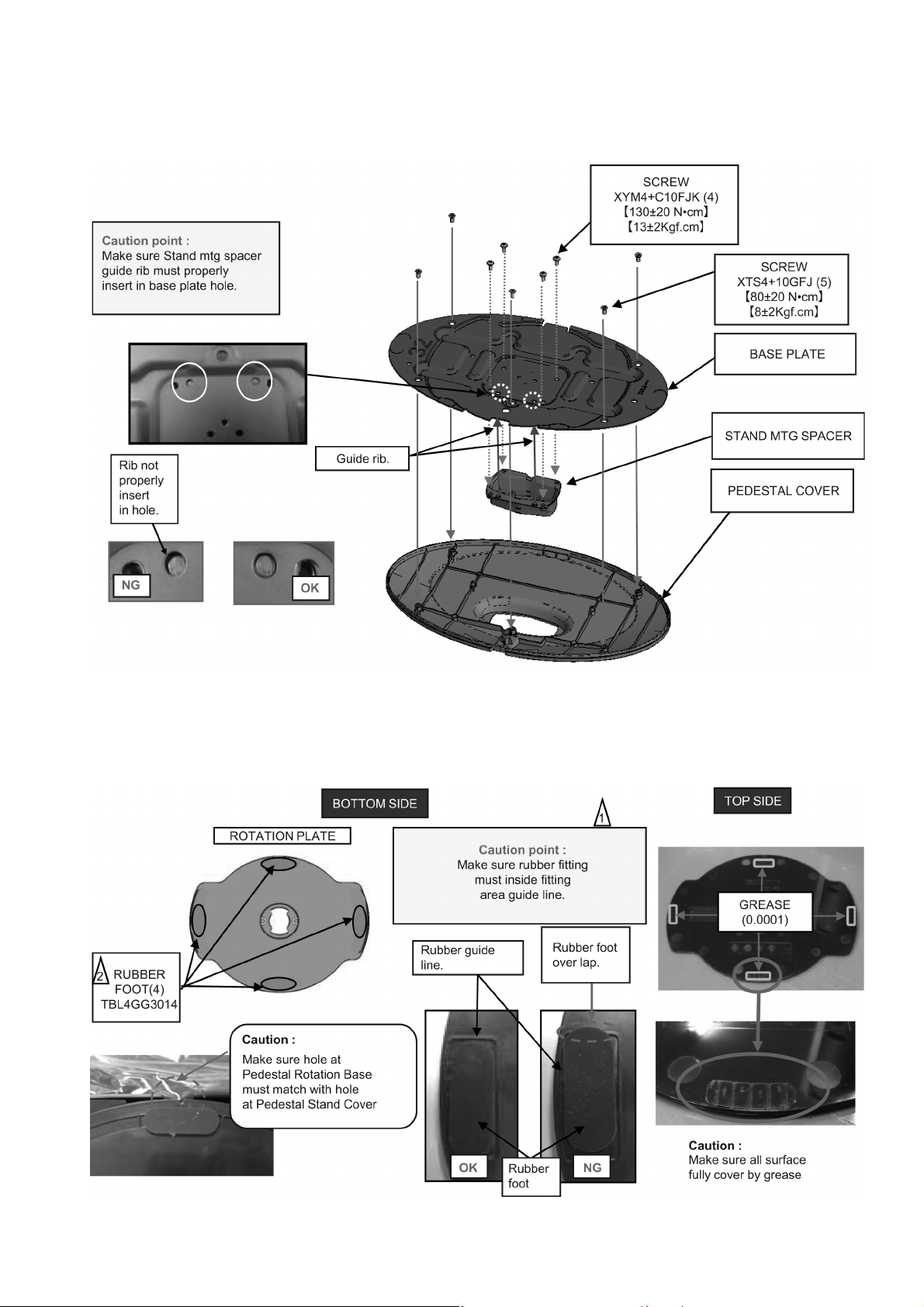
7.17. Pedestal Assembly 1
Step 1
Setting PEDESTAL COVER and STAND MTG SPACER and BASE PLATE with SCREWS.
TH-L32A20X
Step 2
1. Stick the RUBBER FOOT at bottom ROTATION PLATE.
2. Make sure ROTATION PLATE surfacefully cover by grease. Follow the picture.
31
Page 32
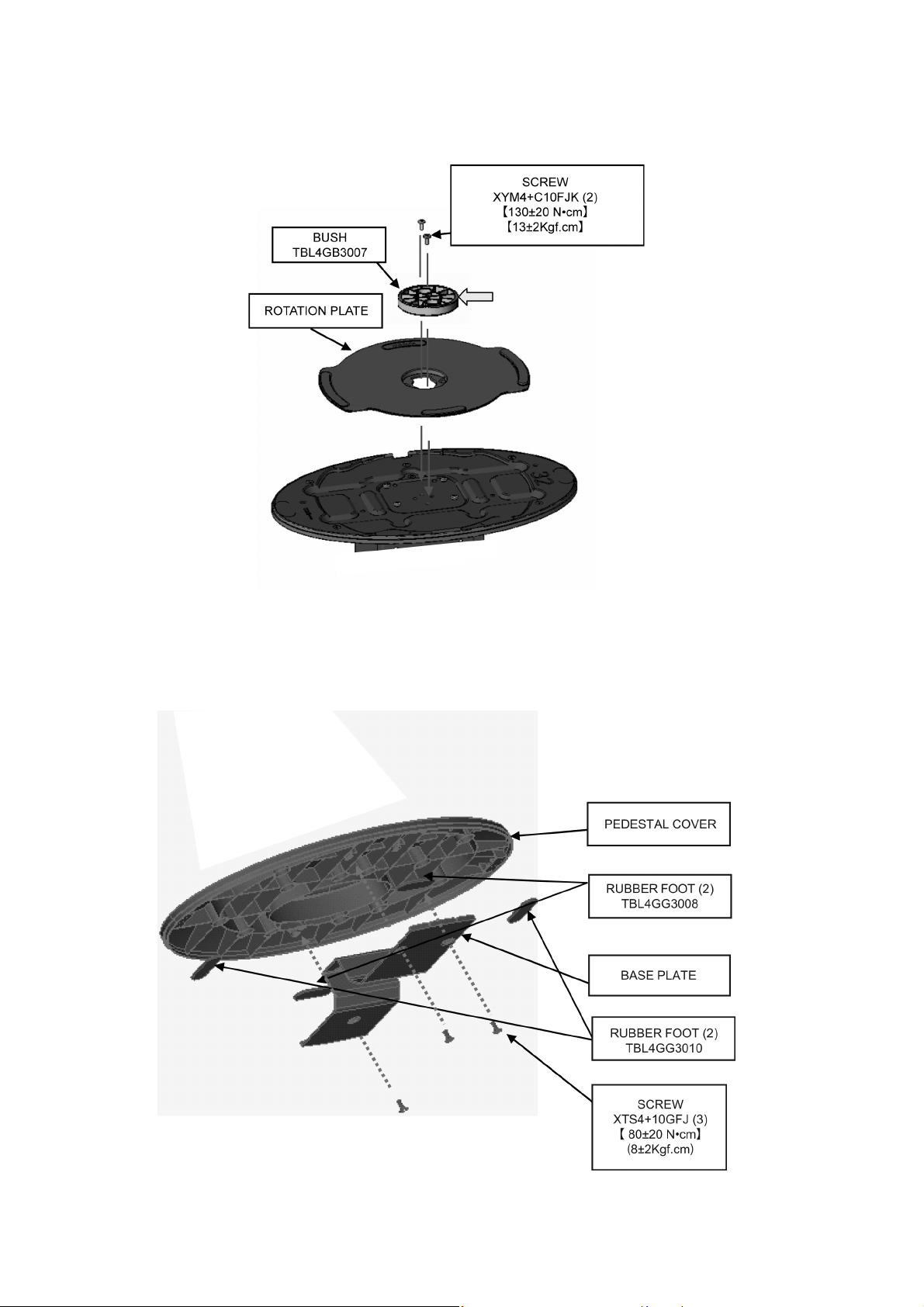
TH-L32A20X
7.18. Pedestal Assembly 2
Step 3
Setting ROTATION PLATE and BUSH with SCREWS.
7.19. Pedestal Assembly 3
Step 1
Setting BASE PLATE and PEDESTAL COVER with SCREWS.
32
Page 33
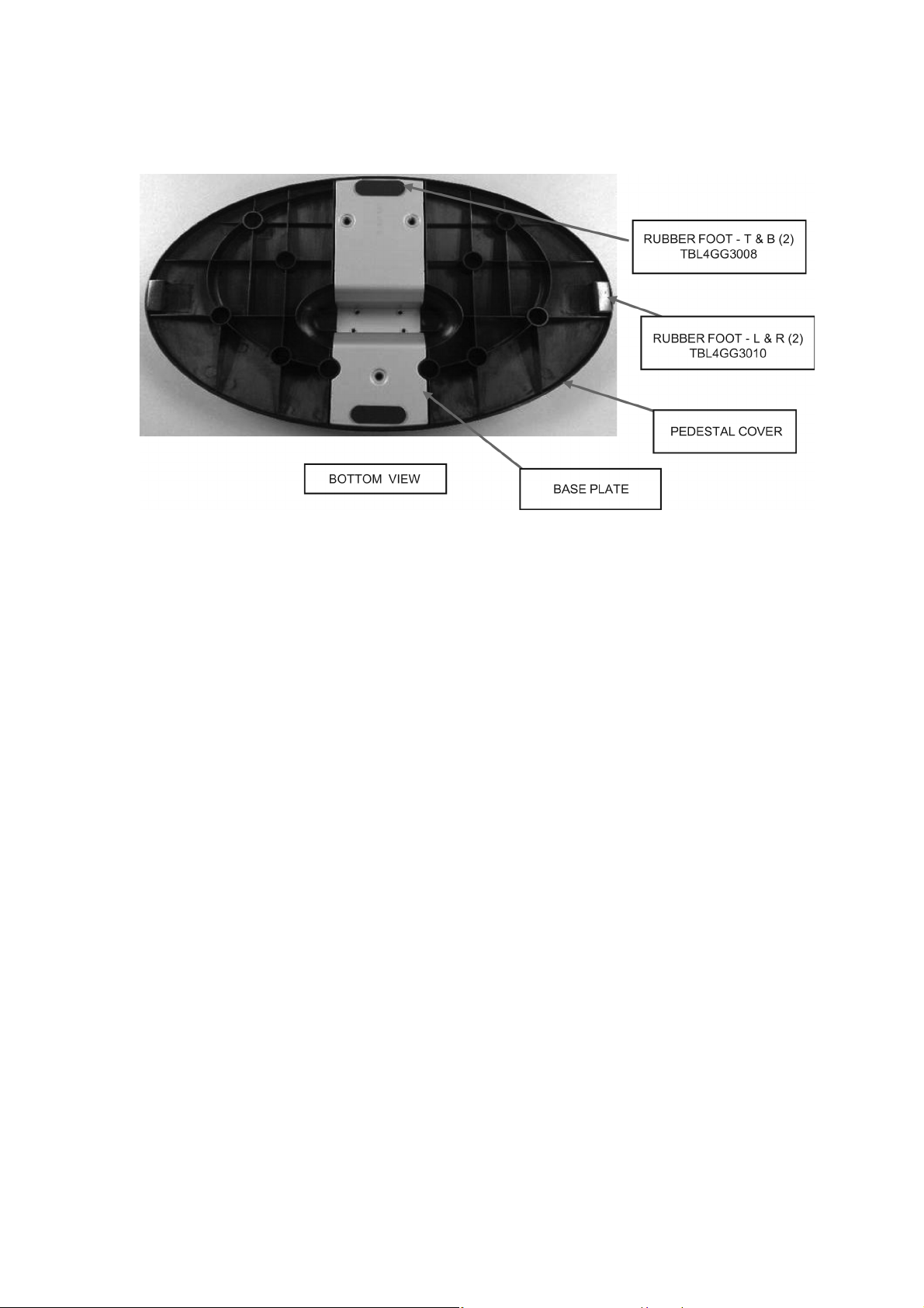
Step 2
1. Stick the RUBBER FOOT at bottom PEDESTAL COVER and BASE PLATE.
2. RUBBER FOOT (TBL4GG3008 - 2 pcs) stick at BASE PLATE.
3. RUBBER FOOT (TBL4GG3009 - 2 pcs) stick at bottom PEDESTAL COVER.
TH-L32A20X
33
Page 34
TH-L32A20X
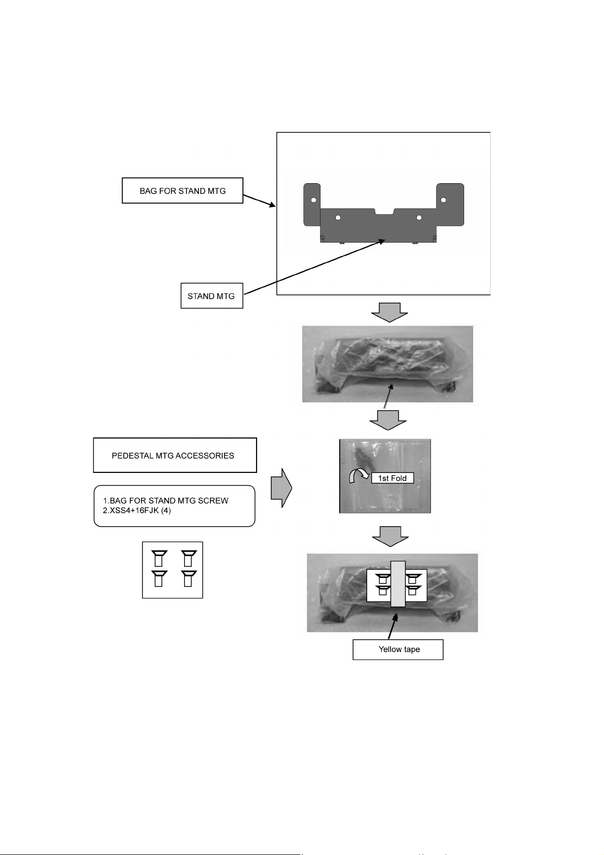
7.20. Stand MTG Assembly
(Refer each part no. to part list)
1. STAND MTG are put in BAG.
2. BAG is wrapped around STAND MTG.
3. SCREW is put in the BAG and use yellow tape to hold screw bag.
34
Page 35
8 Measurements and Adjustments
8.1. Voltage chart of A-board
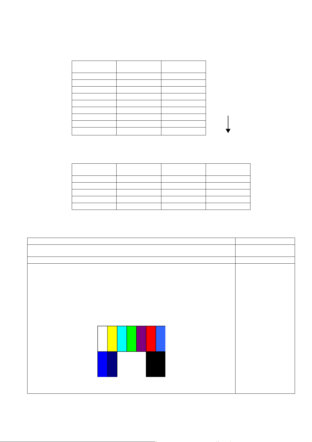
Check voltage as follows at Reception state
VOLTAGE TEST POINT SPECIFICATION
(Reception state)
STB3.3V TP4716 3.3 ± 0.16 V
SUB5V TP4724 5 ± 0.25 V
SOUND15V TP2765 18 ± 2 V
5VS TP2768 6.1 ± 0.3 V
SUB6V TP2767 6.1 ± 0.3 V
TCON13.7V TP7019 12.5 ± 2 V only miniLVDS model
TCON2.5V TP4826 2.5 ± 0.12 V
TCON31V TP7013 31 ± 3.1 V
TCON-6V TP7014 -5.7 ± 0.6 V
8.2. Voltage chart of P-board
TH-L32A20X
VOLTAGE TEST POINT SPECIFICATION
(Reception state)
P32V TP7503 31 ± 2.5 V J107
17V TP7502 18 ± 2 V J115
DTV12V TP7501 12.2 ± 0.6 V J21
TUNER6V TP7601 6.1 ± 0.3 V D7603K
DC390V TP7201 390 ± 10 V
TEST POINT
8.3. Picture level adjustment (RF)
Instrument Name Remarks
1. REMOTE TRANSMITTER
2. Ex. Signal (Sprit color bar)
Adjustment or Inspection Procedure Remarks
<procedure>
1. Receive the Sprit color bar.
(Screen mode: ZOOM or FULL Picture mode: DYNAMIC AI: OFF AI Picture: OFF)
*BACK LIGHT +30
<Inspection>
1. Enter Service mode, and select MAIN_ADJ PICTURE.
Volume UP/DOWN key makes GAIN displayed under PICTURE to set.
Pushing the remote controller [OK] key for about 3 seconds, GAIN is suited
to the adjustment value automatically.
(The Sprit Color Bar Pattern)
35
Page 36
TH-L32A20X
8.4. Picture level adjustment (VIDEO)
Instrument Name Remarks
1. REMOTE TRANSMITTER
2. Video signal generator (100% Color bar)
Adjustment or Inspection Procedure Remarks
<procedure>
1. Receive 100% Color bar.
(ASPECT: ZOOM or FULL, Picture mode: VIVID, AI Picture: OFF)
* BACK LIGHT MAX VALUE
<Inspection>
1. Enter Service mode, and select ADJUST CONTRAST.
Volume UP/DOWN key makes GAIN value displayed on the right of CONTRAST to set.
Pushing the remote controller [OK] key for about 3 seconds, GAIN is suited to the adjustment value
automatically.
8.5. Picture level adjustment (YUV)
Instrument Name Remarks
1. REMOTE TRANSMITTER
2. Component Video signal generator (100% Color bar 1080i)
Adjustment or Inspection Procedure Remarks
<procedure>
1. Receive 100% Color bar.
(ASPECT: ZOOM or FULL, Picture mode: VIVID, AI Picture: OFF)
* BACK LIGHT MAX VALUE
<Inspection>
1. Enter Service mode, and select ADJUST CONTRAST.
Volume UP/DOWN key makes GAIN value displayed on the right of CONTRAST to set.
Pushing the remote controller [OK] key for about 3 seconds, GAIN is suited to the adjustment value
automatically.
36
Page 37
9 Block Diagram
(LED:7TIMES)
(LED:1TIMES)
(LED:4TIMES)
(LED:
3TIMES)
(LED:9TIMES)
(LED:3TIMES
)
STB5V
TMDS DATA
DCDC
V10
STB_RESET
TUNER5V
INV_SOS
OVP_DET
ERROR DET
TUNER5V
(SIDE)
POWER LED(R)
DTV12V
POWER
CONTROL
LCD PANEL
TUNER6V
STB3.3V
INV_SOS
STB5.8V
DCDC
D/A
RECTIFIER
+5.8VS
SUB5V
PANEL POWER SOS
VOFF2-6V
SUB9V
(SIDE)
DCDC
V
SUB9V
SOUND SOS
STB_RESET
DVDD2.5V
AMP
DCDC
SOUND SOS
STB3.3V
VCON31V
INV_ON
(STM)
(SIDE)
DTV_L/R
DROP
D/A
CONVERTOR
SUB1.2V
STB5V
CONTROL PANEL
DVB_CVBS
R
L/R
HDMI I/F
PFC
CONTROL
V-BOARD
ANALOG-ASIC
Y/PB/PR,
R/G/B/H/V CVBS
VOLTAGE
HDMI3
V/Y/PB/PR
STANDBY
VOLTAGE
RECTIFIER
C.A.T.S. SENSOR
V
DTV12V SENSE
INV_ON
SUB3.3V
PANEL POWER SOS
OPTICAL AUDIO OUT
DCDC
DVDD2.5V
OVP_DET
DCDC
DTV12V
INVERTER
POWER
CONTROL
CURCUIT
PWM
SUB1.8V
VIDEO
PROCESSOR
STB+3.3V
SUB5V
R/G/B/H/V
PWM
VREF_1-12
REMOTE RECEIVER
OVER
AC CORD
STB+3.3V
12V
SUB 3.3V SENSE
AUDIO
PANEL
EEPROM
AUDIO
PROCESSOR
SUB_ON
TS Parallel
SD CARD DATA
OPERATION
BUTTON
VOLTAGE
K-BOARD
HDMI2
A02
EEPROM
K01
NAND
FLASH
DVDD2.5V
ON
HDMI1
LIVE
+5.8VS
INV_PWM
TMDS DATA
POWER LED
INV_PWM
INV_SOS
SUB1.8V
SPEAKER(R)
(A Chip)
AV2
CPU BUS
I/F
(D Chip)
CONTROL
DCDC
NEUTRAL
17V
SOS DET
A-BOARD
PANEL
OPTICAL OUT
SUB_ON
SOS DET
AV SW
AVDD13.7V
PC
MONITOR L,R
POWER LED
P-BOARD
POWER SUPPLY
MONITOR
OUT
MONITOR V
DIGITAL SIGNAL PROCESSOR
OPTICAL
V
REMOTE RECEIVER
A/D
CONVERTOR
AVDD13.7V
P5,P6.P7,P8
C.A.T.S. SENSOR
AVDD13.7V
RECTIFIER
LINE
FILTER
SOUND17V
AUDIO
A14
SPEAKER(L)
HP
AV3
HEADPHONE
CPU BUS
INV_PWM
SD CARD
OUT
AV1
SUB
ON/OFF
L
+5.8VS
RECEIVER
L/R
HOT START
(DAC_ENB)
SD CARD DATA
TMDS DATA
PROCESS
VOLTAGE
RECTIFIER
REMOTE IN
L/R
RELAY
32V
DTV12V
Peaks sLD
SOUND17V
TS Parallel
SIF
SUB5V
STB+5.8V
SLOT
SUB3.3V
LVDS DATA
POWER SW
P2
L/R
P1
BACK LIGHT
DCDC
SUB1.2V
A10
LVDS DATA
INV_ON
STB5V
KEYSCAN
A09
A12
C.A.T.S. SENSOR
IFD_OUT
OFDM
SIF_OUT
TUNER
V
(LED:7TIMES)
(LED:1TIMES)
(LED:4TIMES)
(LED:3TIMES)
(LED:9TIMES)
(LED:3TIMES)
9.1. Main Block Diagram
TH-L32A20X
37
Page 38
TH-L32A20X
10 Wiring Connection Diagram
38
Page 39
TH-L32A20X
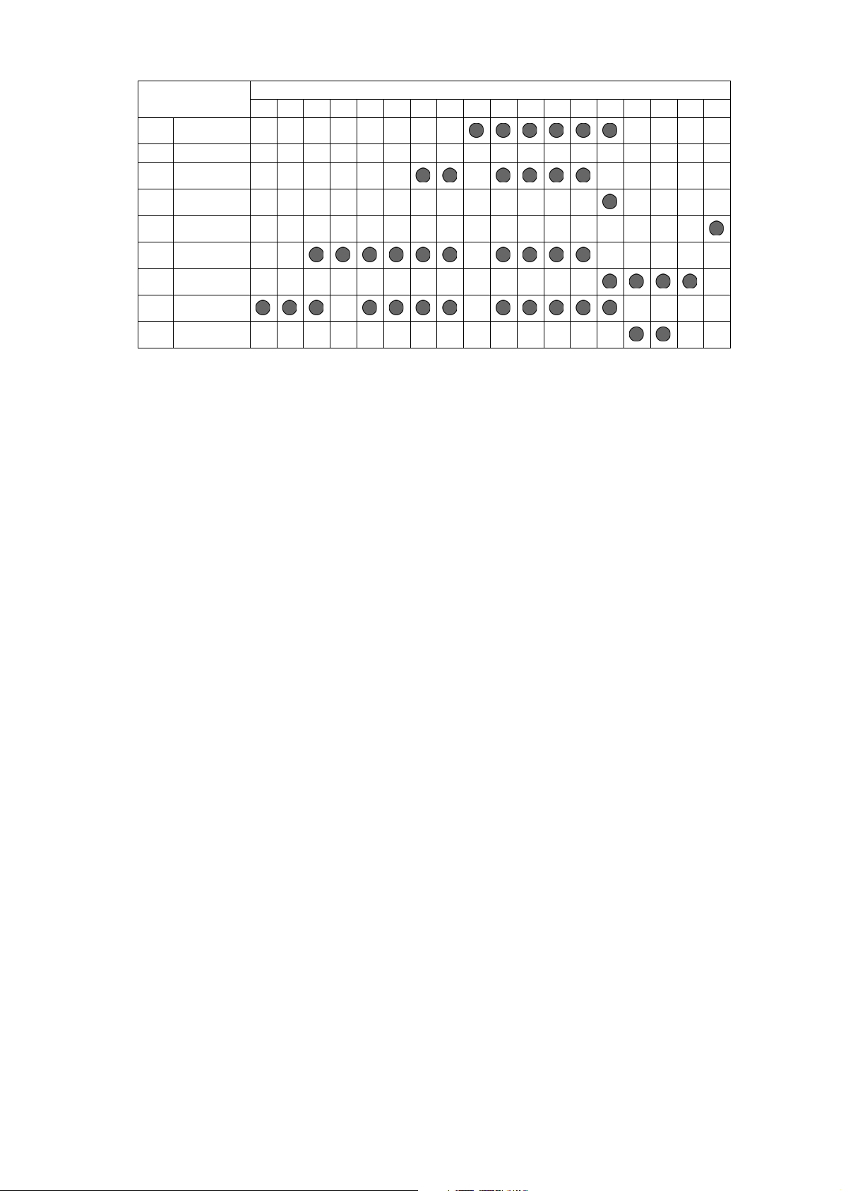
Wire
No.1 A10 - V10
No.2 A04 - K01
No.3 A11 - SP (L)
No.4 A11 - SP (R)
No.5 P2 - A03
No.6 A25 - TW (L)
No.7 A25 - TW (R)
No.8 A13 - L13 (L)
No.9 A13 - L13 (R)
Clamper
123456789101112131415161718
39
Page 40
TH-L32A20X
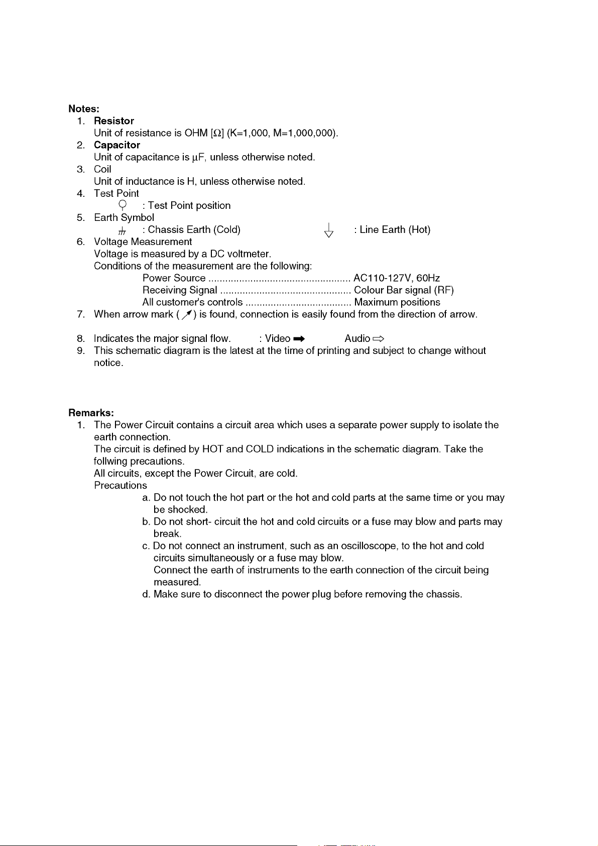
11 Schematic Diagram
11.1. Schematic Diagram Notes
40
Page 41
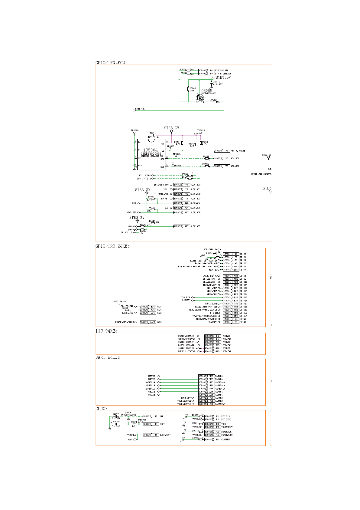
11.2. A Board
<1A>
<2A>
11.2.1. A Board - Sheet : 002 (1 / 4)
TH-L32A20X
41
Page 42
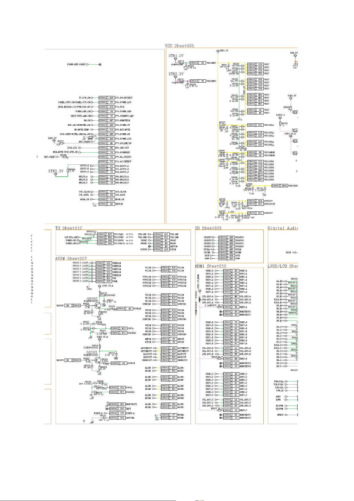
TH-L32A20X
<1B>
<2B>
<3B>
<4B>
<1A>
<2A>
11.2.2. A Board - Sheet : 002 (2 / 4)
42
Page 43
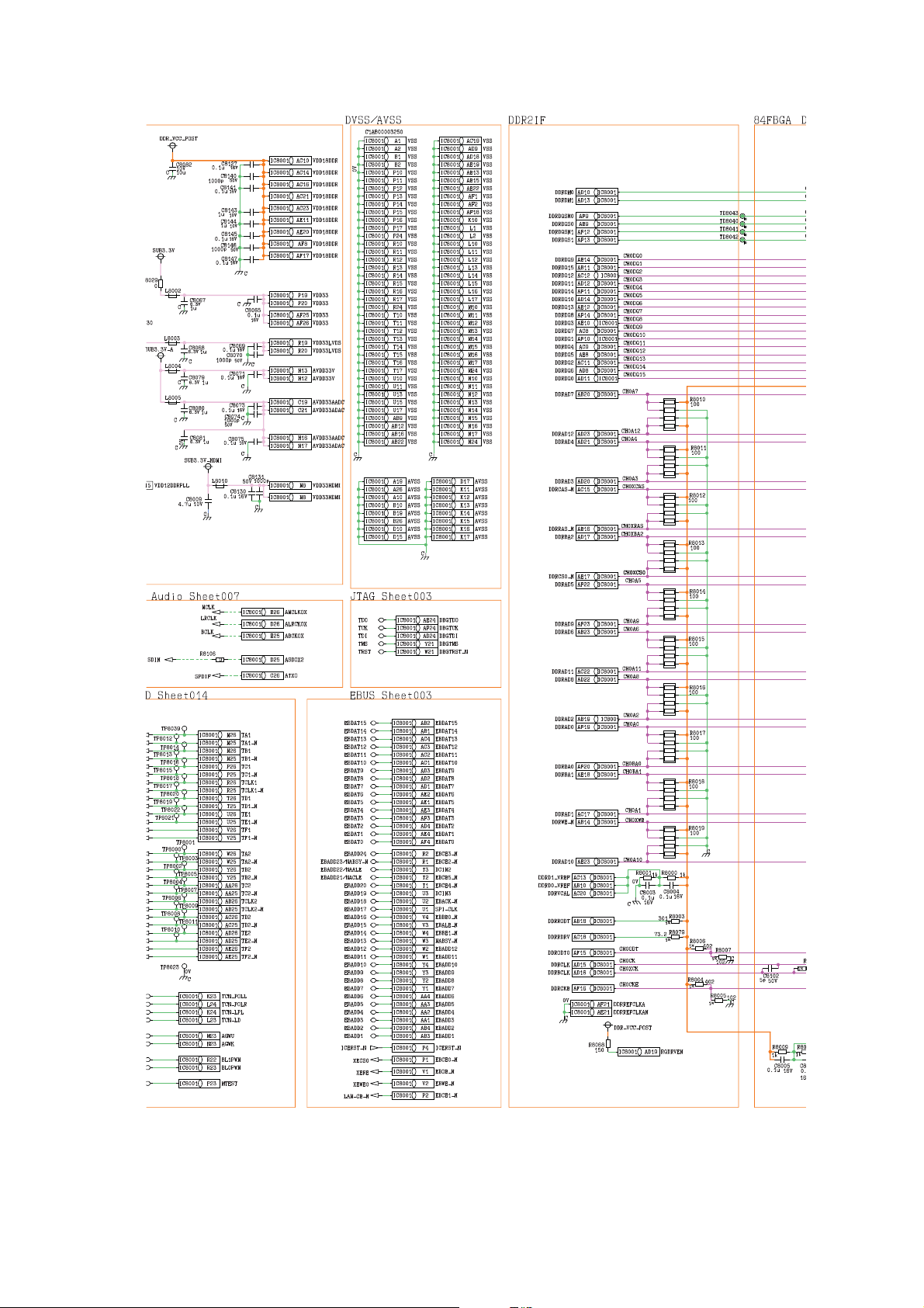
11.2.3. A Board - Sheet : 002 (3 / 4)
<1C>
<2C>
<3C>
<4C>
<5C>
<6C>
<7C>
<1B>
<2B>
<3B>
<4B>
TH-L32A20X
43
Page 44
TH-L32A20X
<1C>
<2C>
<3C>
<4C>
<5C>
<6C>
<7C>
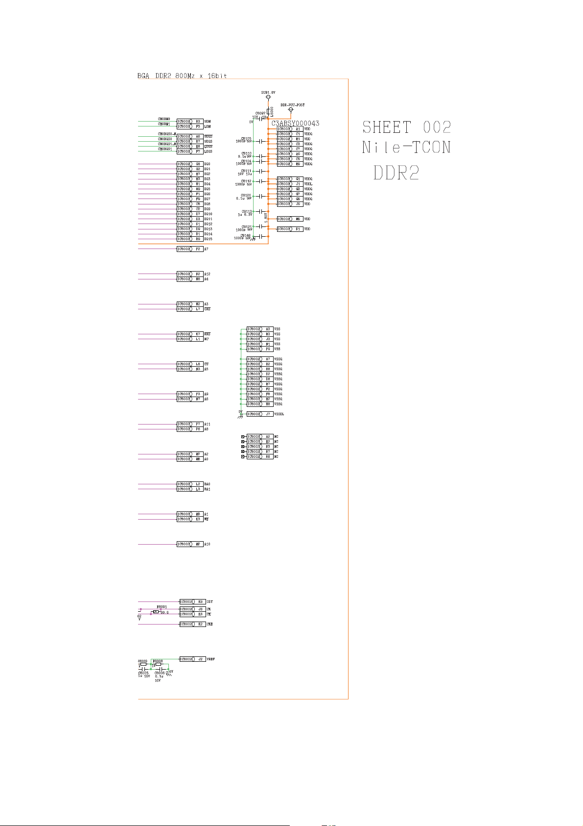
11.2.4. A Board - Sheet : 002 (4 / 4)
44
Page 45
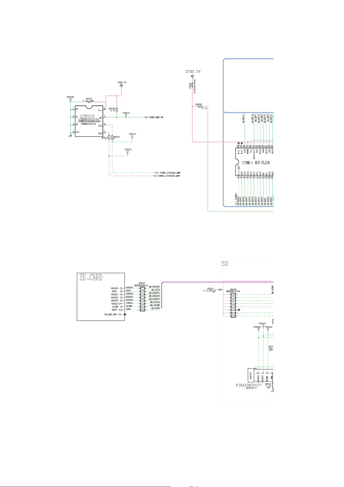
11.2.5. A Board - Sheet : 003 (1 / 3)
<1A>
<2A>
<3A>
<4A>
<5A>
<6A>
<7A>
TH-L32A20X
45
Page 46
TH-L32A20X
<1B>
<2B>
<3B>
<4B>
<5B>
<1A>
<2A>
<3A>
<4A>
<5A>
<6A>
<7A>
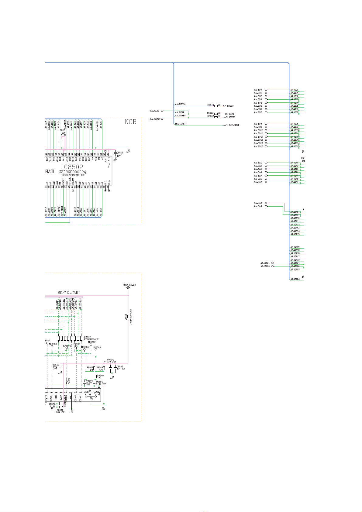
11.2.6. A Board - Sheet : 003 (2 / 3)
46
Page 47
<1B>
<2B>
<3B>
<4B>
<5B>
TH-L32A20X
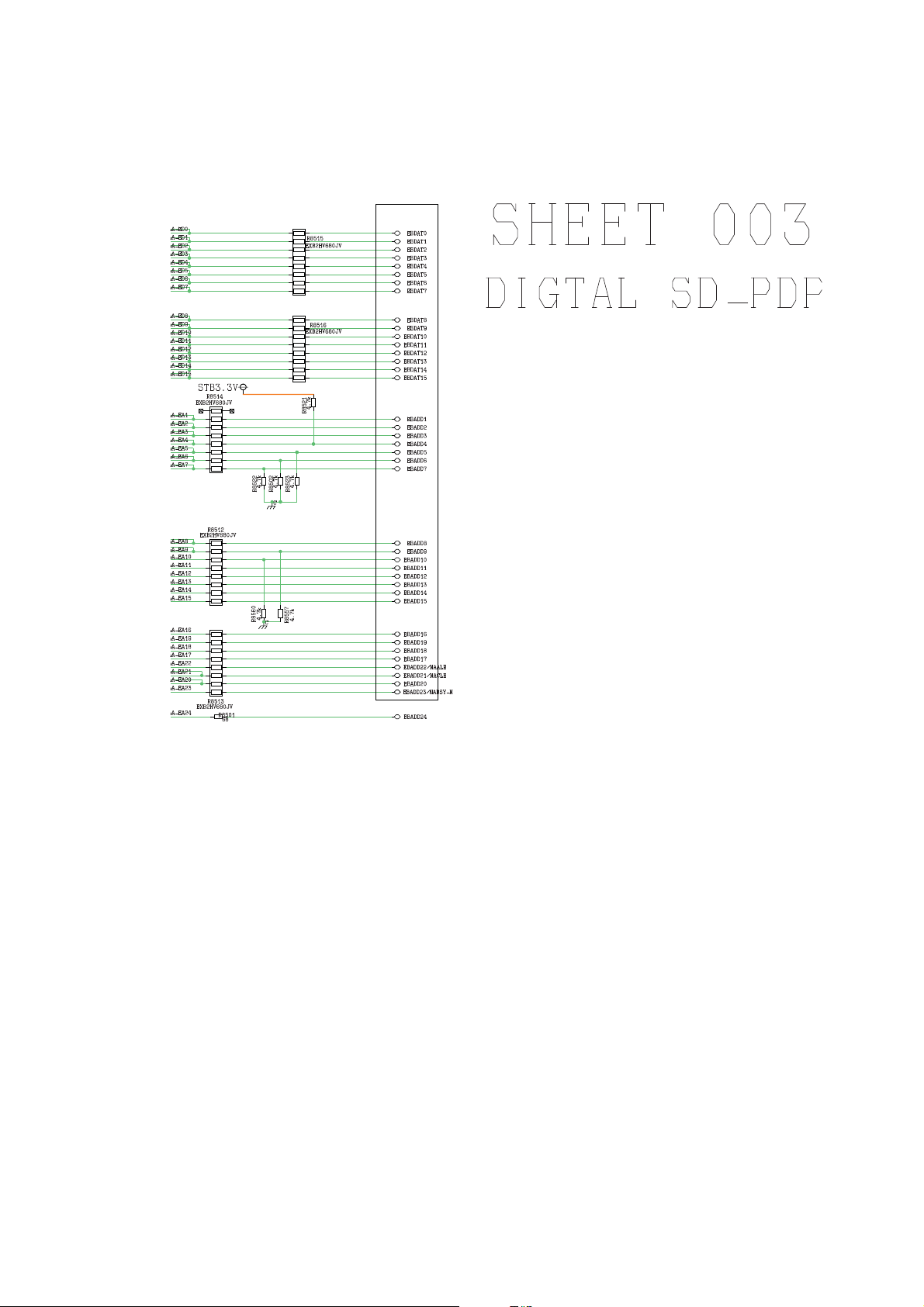
11.2.7. A Board - Sheet : 003 (3 / 3)
47
Page 48
TH-L32A20X
<1A>
<2A>
<3A>
<4A>
<5A>
<6A>
<7A>
<8A>
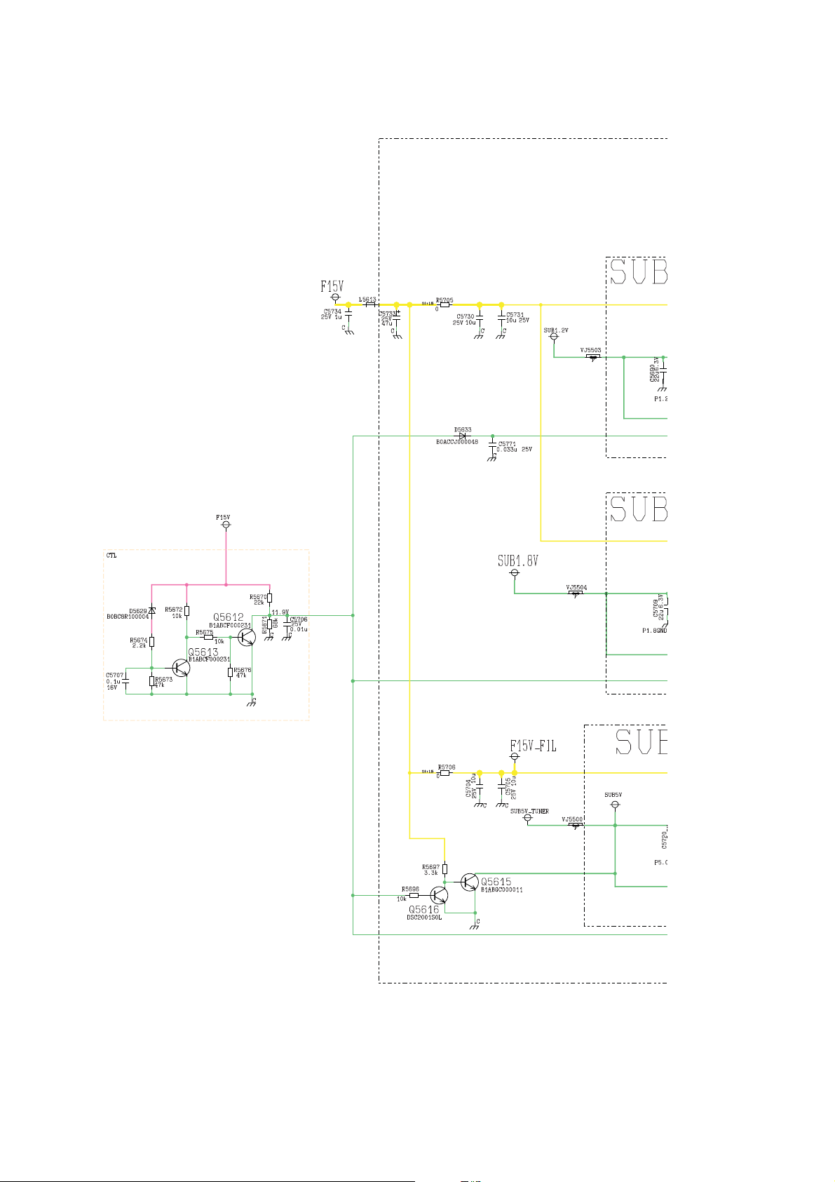
11.2.8. A Board - Sheet : 005 (1 / 3)
48
Page 49
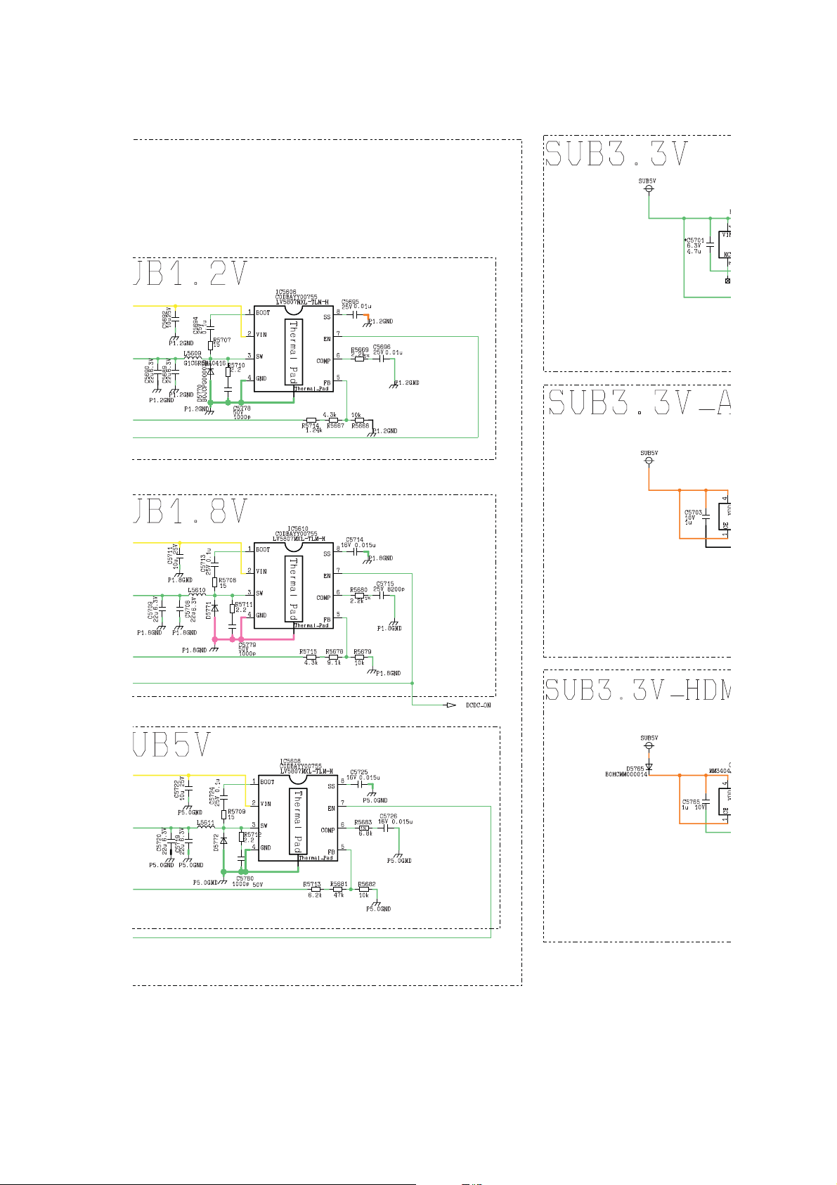
11.2.9. A Board - Sheet : 005 (2 / 3)
<1B>
<2B>
<3B>
<4B>
<1A>
<2A>
<3A>
<4A>
<5A>
<6A>
<7A>
<8A>
TH-L32A20X
49
Page 50
TH-L32A20X
<1B>
<2B>
<3B>
<4B>
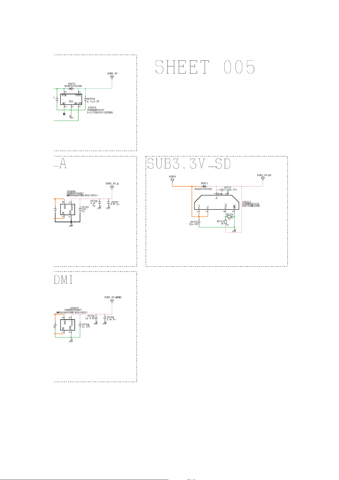
11.2.10. A Board - Sheet : 005 (3 / 3)
50
Page 51
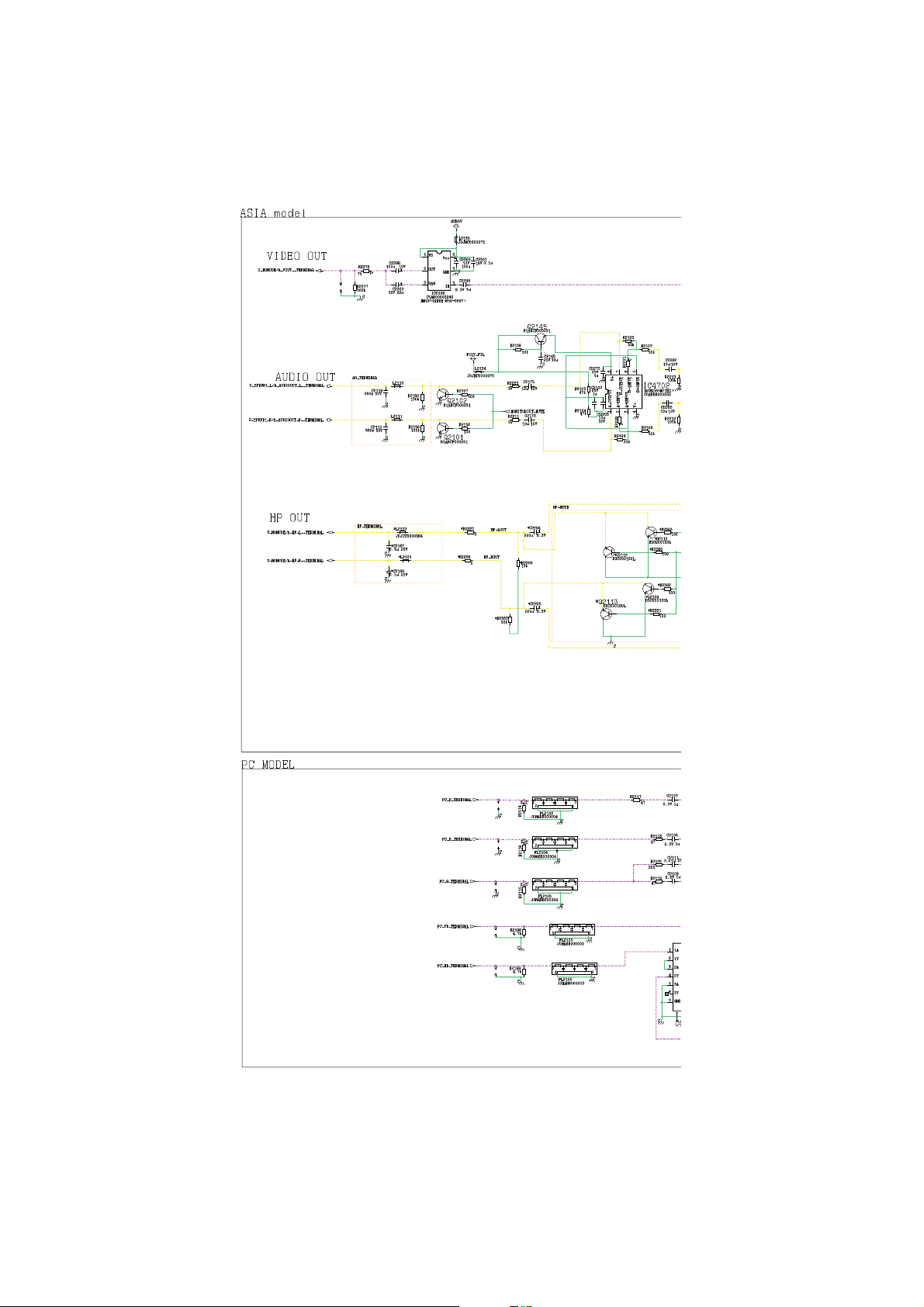
11.2.11. A Board - Sheet : 007 (1 / 4)
<1A>
<2A>
<3A>
<4A>
<5A>
<6A>
TH-L32A20X
51
Page 52
TH-L32A20X
<1B>
<2B>
<3B>
<4B>
<5B>
<6B>
<7B>
<8B>
<1A>
<2A>
<3A>
<4A>
<5A>
<6A>
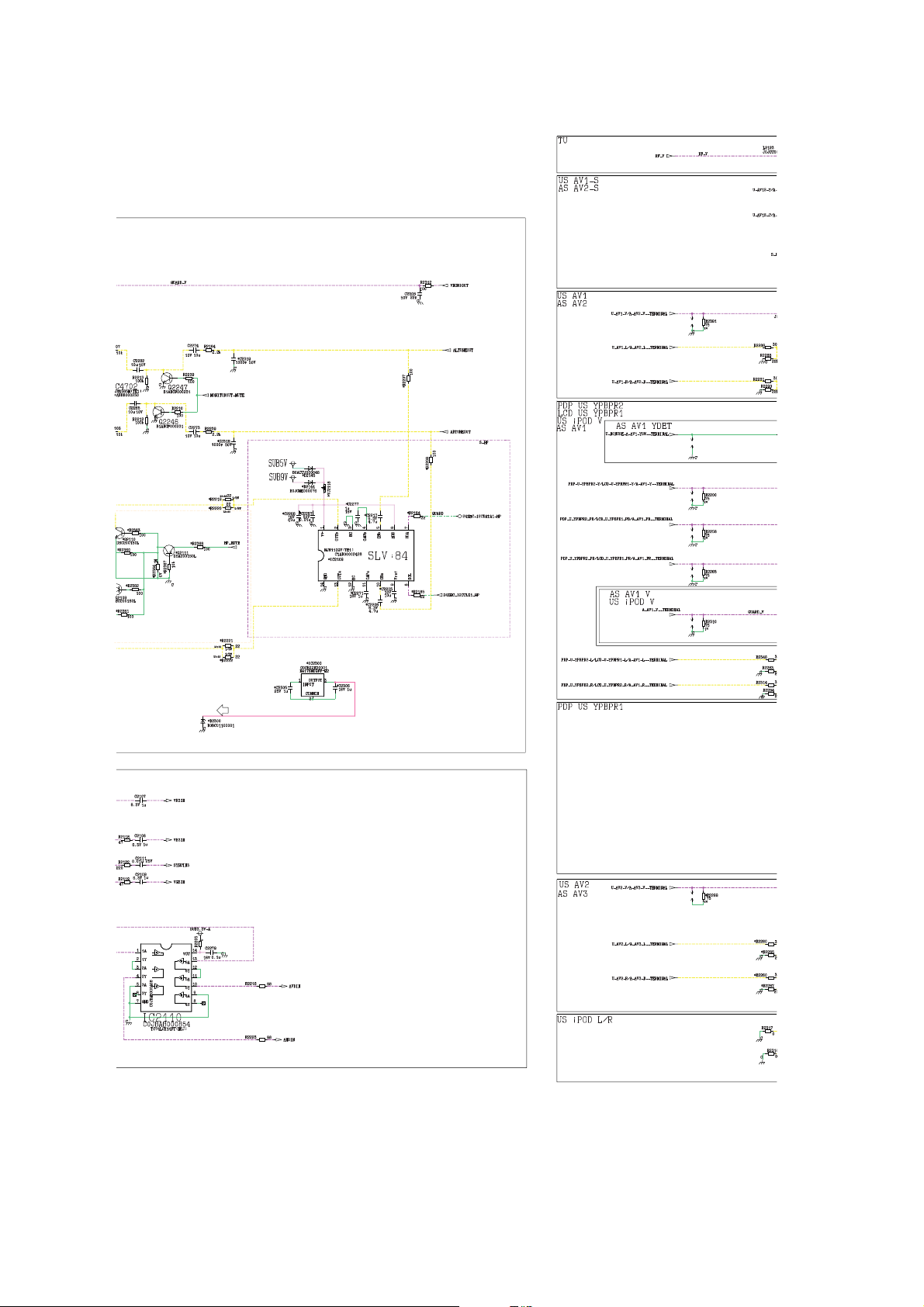
11.2.12. A Board - Sheet : 007 (2 / 4)
52
Page 53
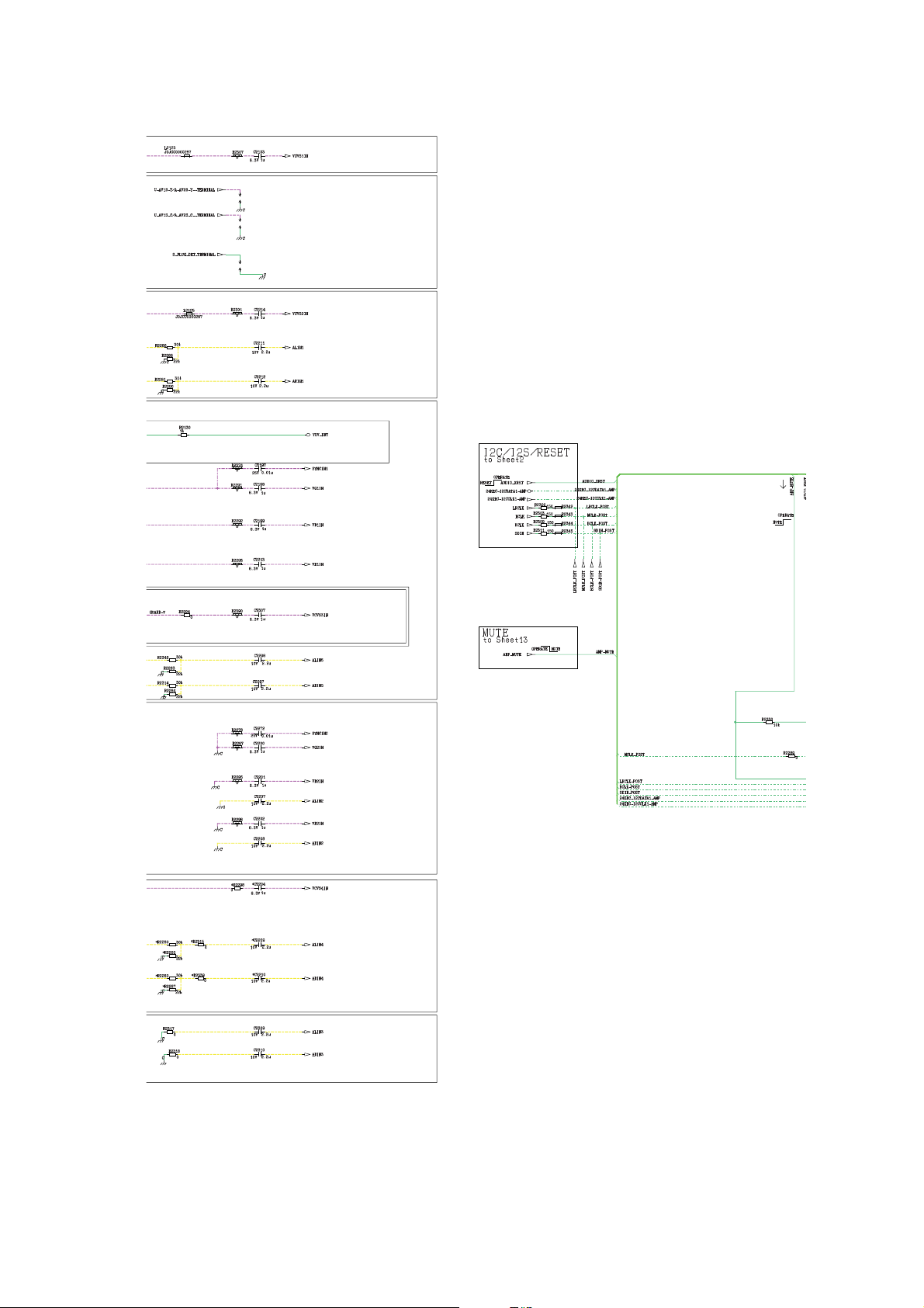
<1C>
<2C>
<1B>
<2B>
<3B>
<4B>
<5B>
<6B>
<7B>
<8B>
TH-L32A20X
11.2.13. A Board - Sheet : 007 (3 / 4)
53
Page 54
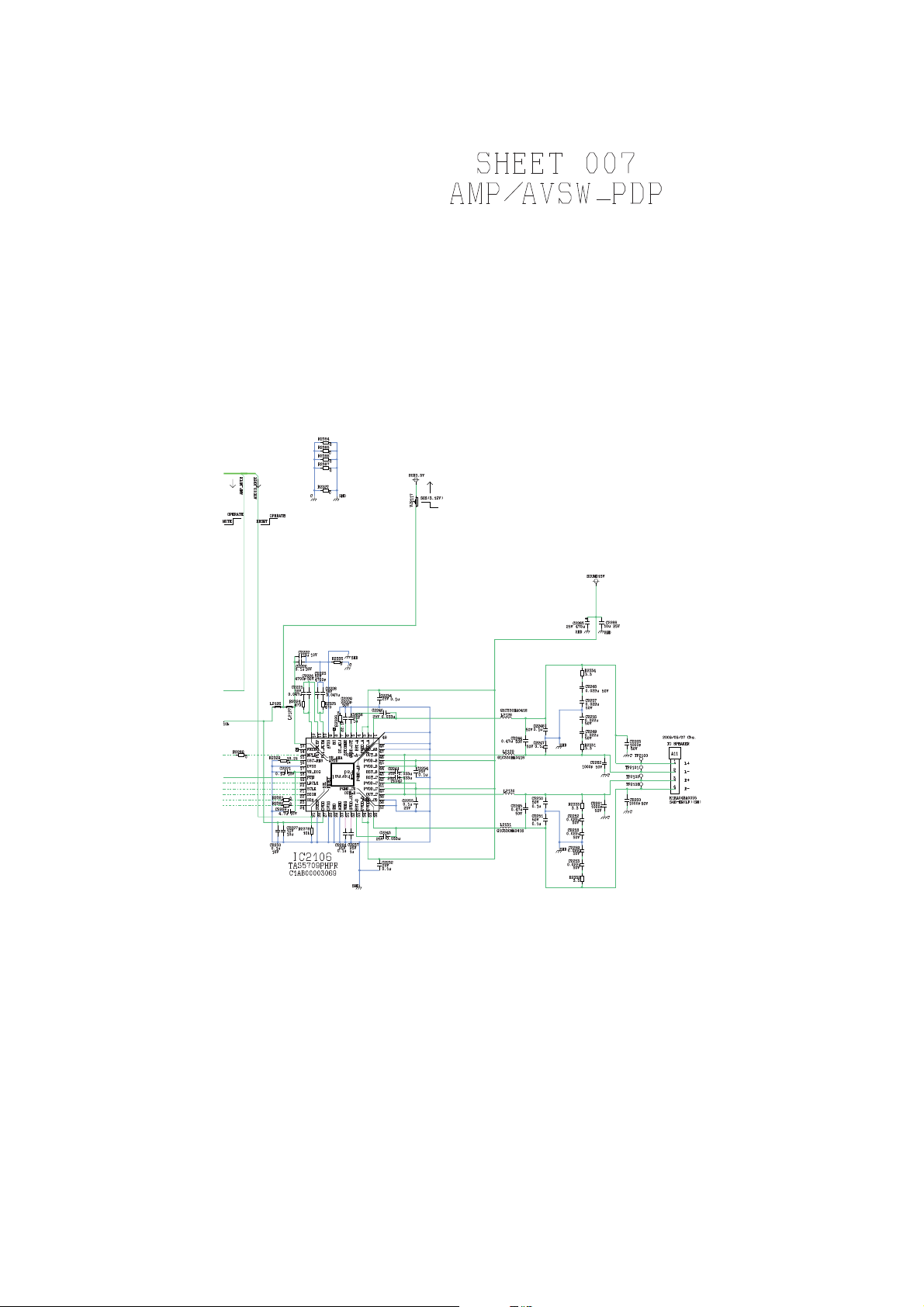
TH-L32A20X
<1C>
<2C>
11.2.14. A Board - Sheet : 007 (4 / 4)
54
Page 55
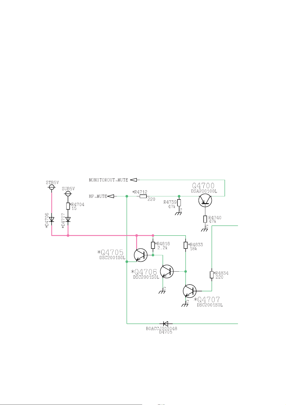
11.2.15. A Board - Sheet : 009 (1 / 4)
TH-L32A20X
<1A>
<2A>
55
Page 56
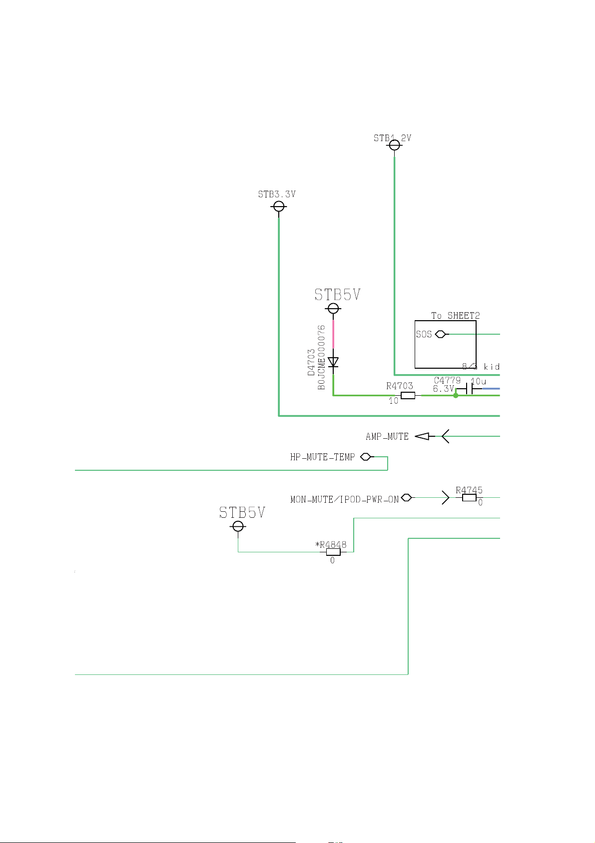
TH-L32A20X
<1B>
<2B>
<3B>
<1A>
<2A>
11.2.16. A Board - Sheet : 009 (2 / 4)
56
Page 57
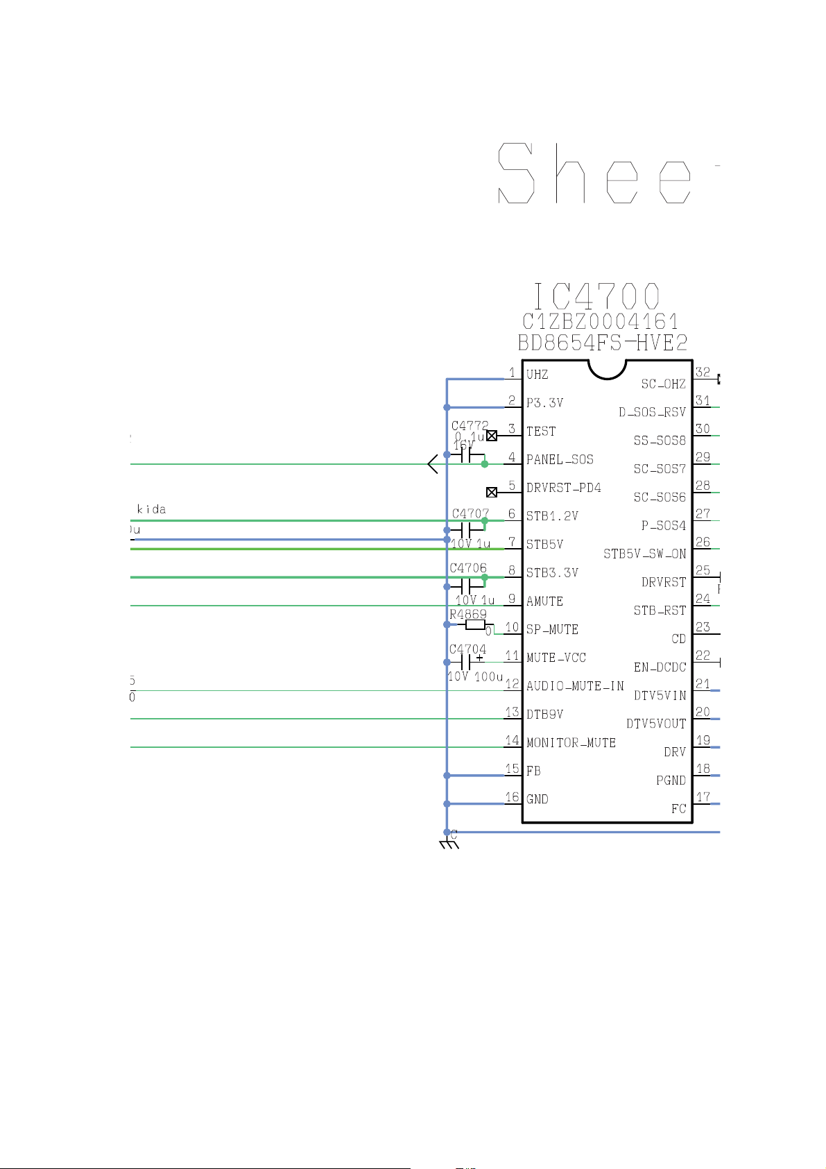
11.2.17. A Board - Sheet : 009 (3 / 4)
<1C>
<1B>
<2B>
<3B>
TH-L32A20X
57
Page 58
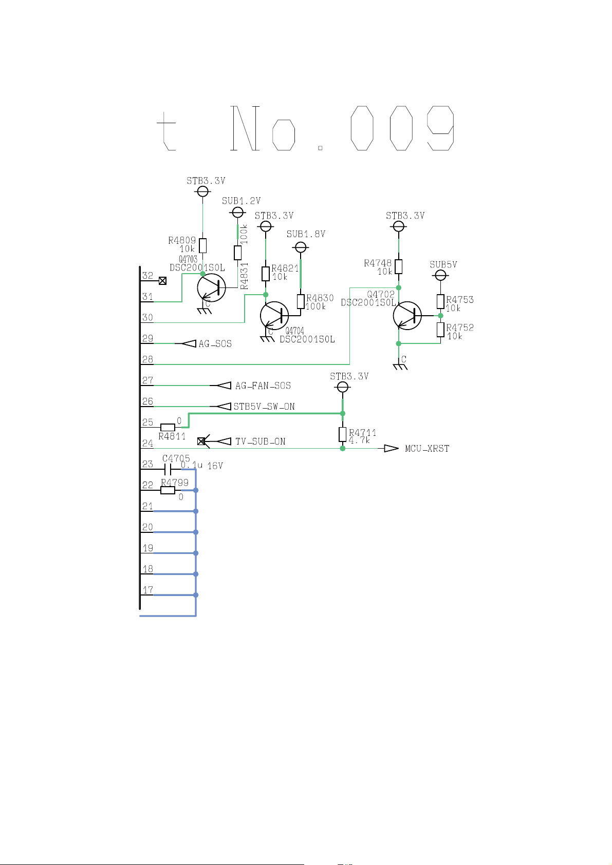
TH-L32A20X
<1C>
11.2.18. A Board - Sheet : 009 (4 / 4)
58
Page 59
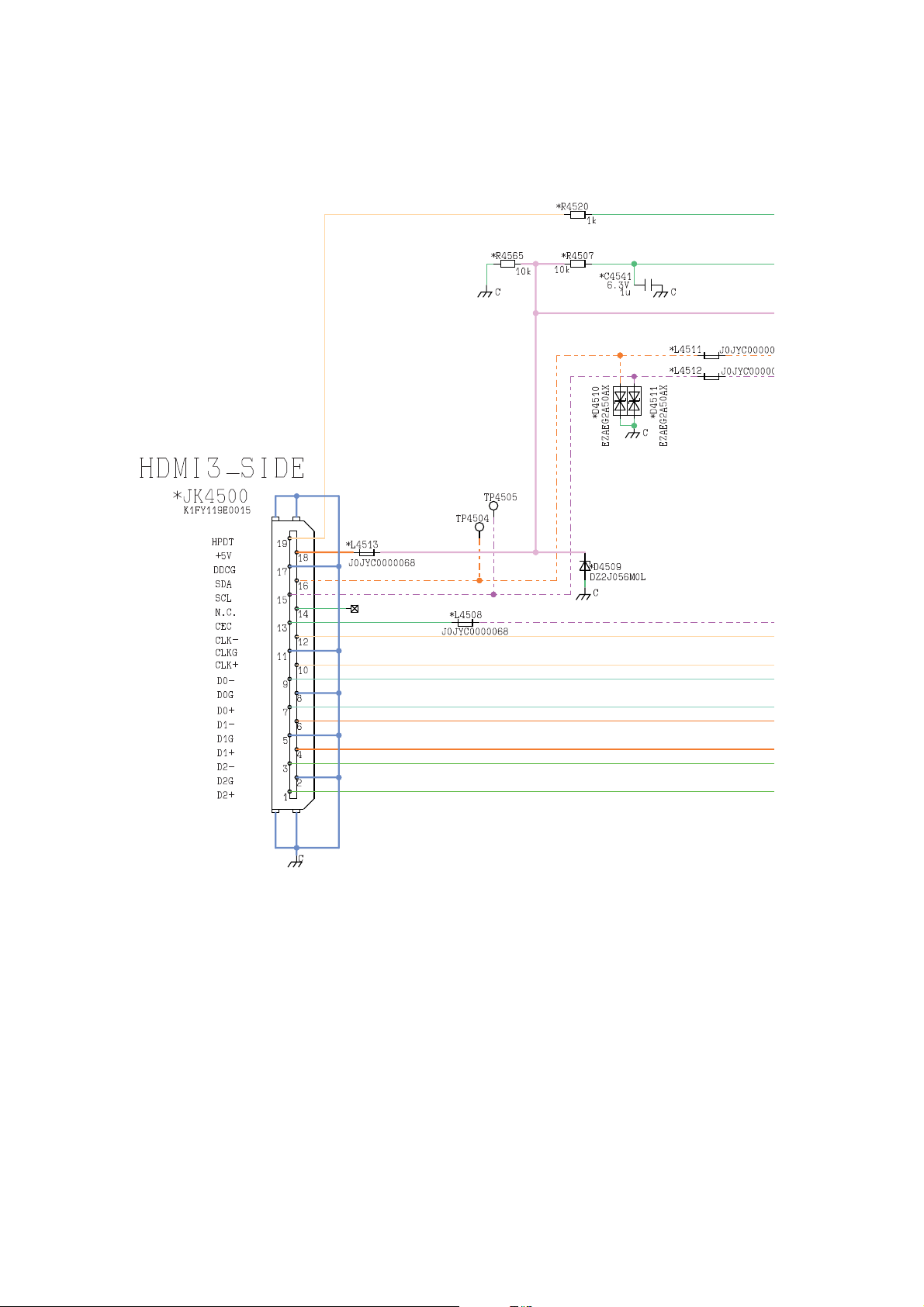
11.2.19. A Board - Sheet : 010 (1 / 6)
TH-L32A20X
<1A>
<2A>
<3A>
<4A>
59
Page 60
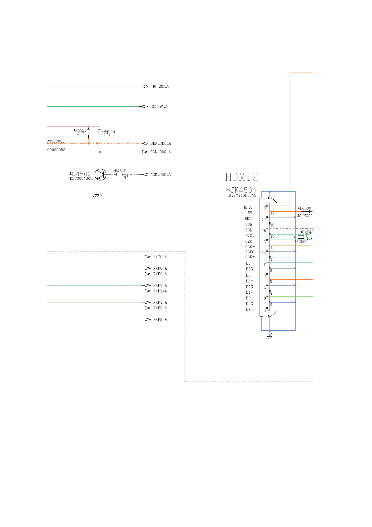
TH-L32A20X
<1B>
<2B>
<3B>
<4B>
<5B>
<1A>
<2A>
<3A>
<4A>
11.2.20. A Board - Sheet : 010 (2 / 6)
60
Page 61
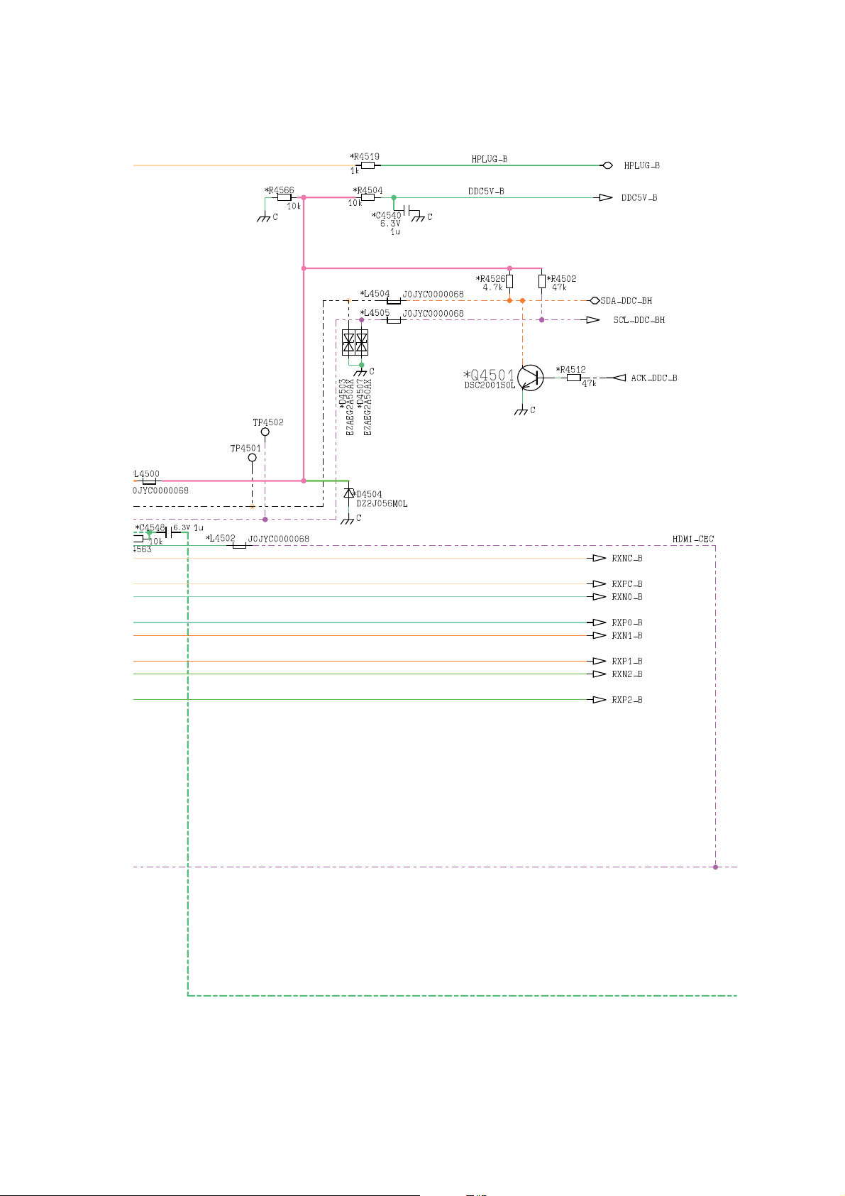
<1C>
<2C>
<1B>
<2B>
<3B>
<4B>
<5B>
TH-L32A20X
11.2.21. A Board - Sheet : 010 (3 / 6)
61
Page 62
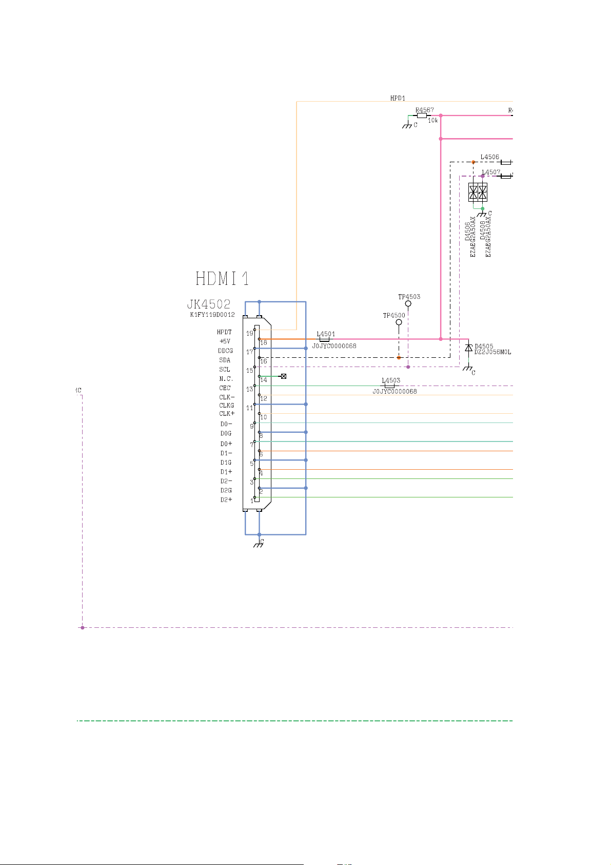
TH-L32A20X
<4D>
<1D>
<2D>
<3D>
<5D>
<1C>
<2C>
11.2.22. A Board - Sheet : 010 (4 / 6)
62
Page 63
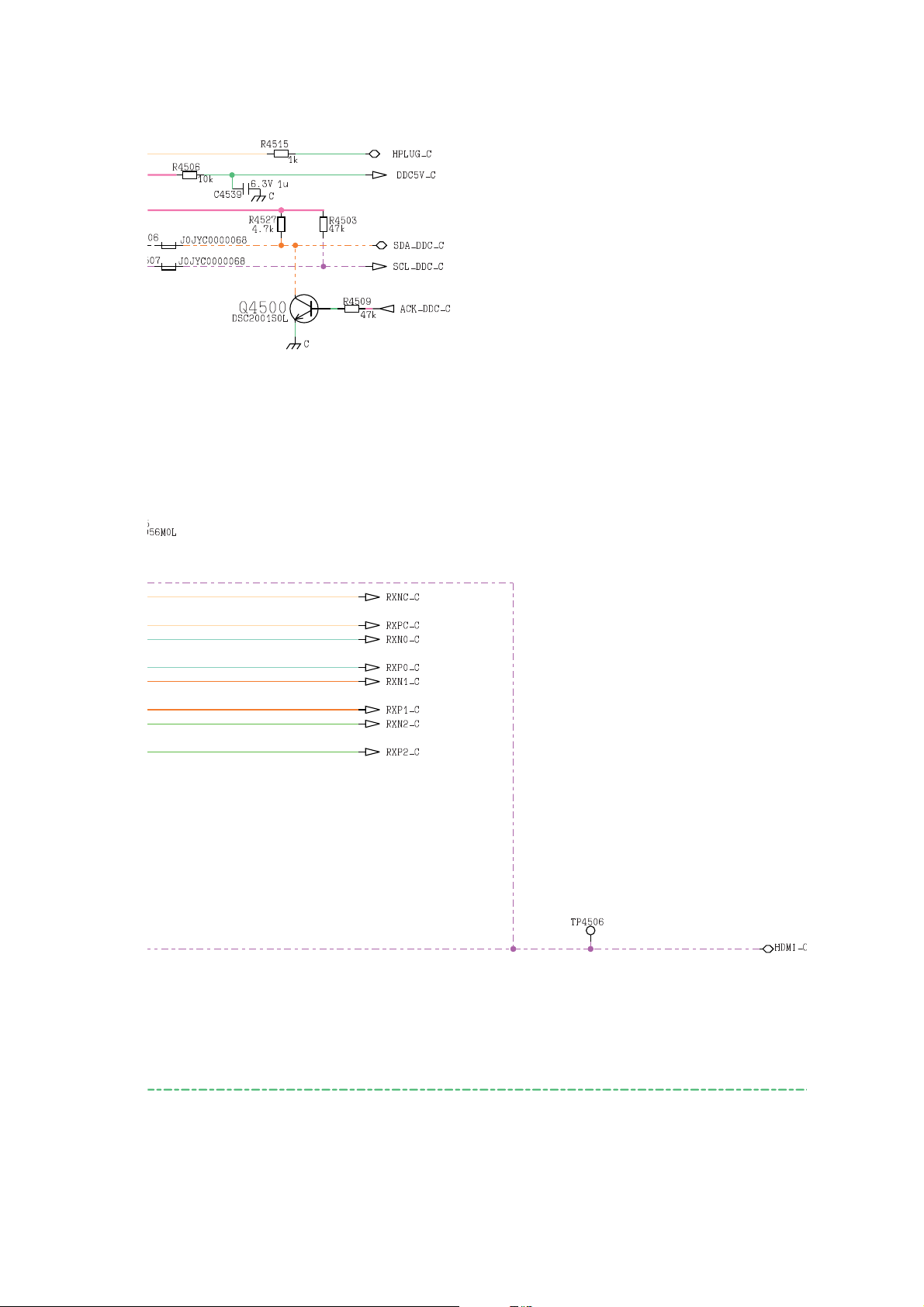
11.2.23. A Board - Sheet : 010 (5 / 6)
<1D>
TH-L32A20X
<2D>
<3D>
<4D>
<5D>
<1E>
63
Page 64
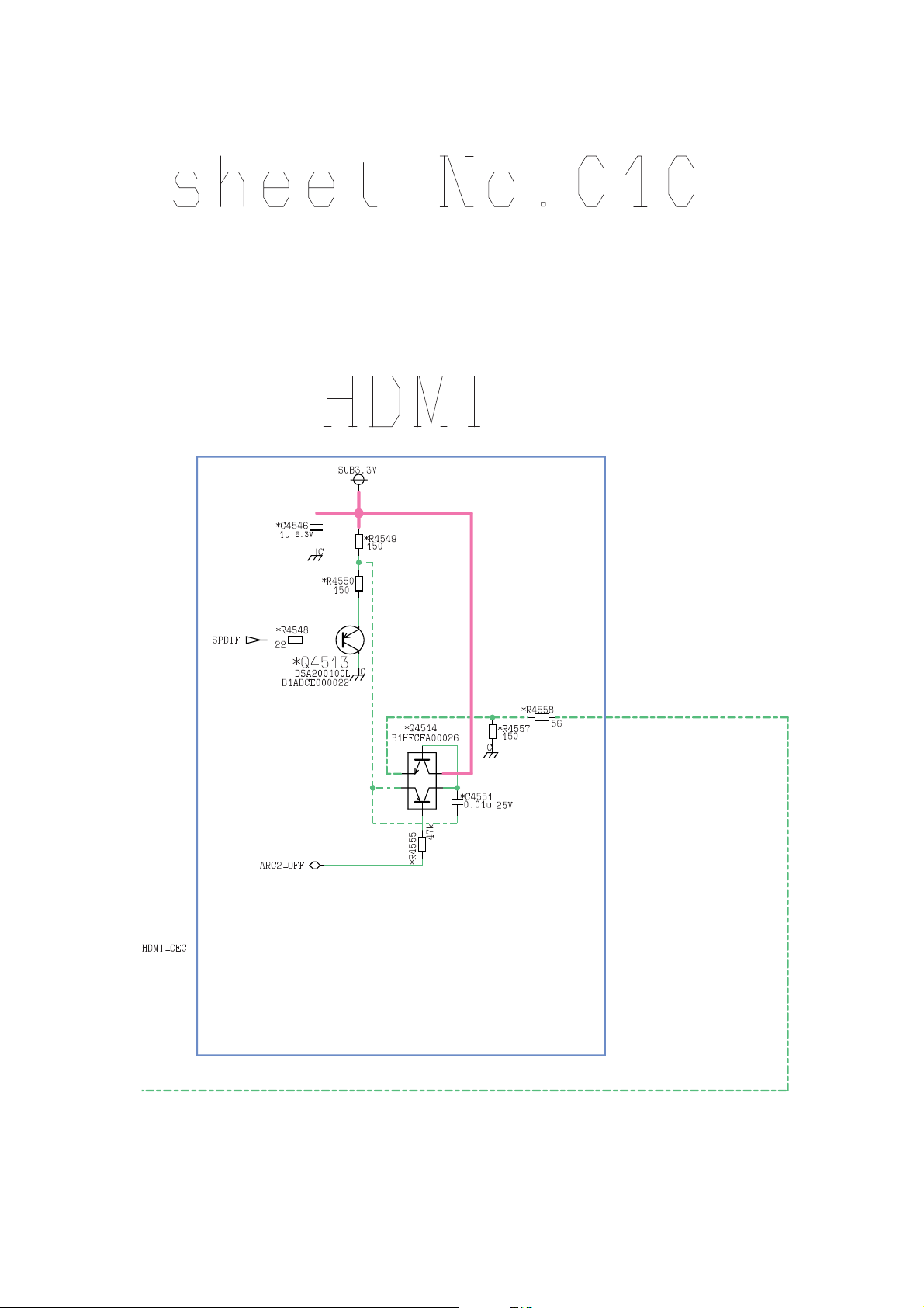
TH-L32A20X
11.2.24. A Board - Sheet : 010 (6 / 6)
<1E>
64
Page 65
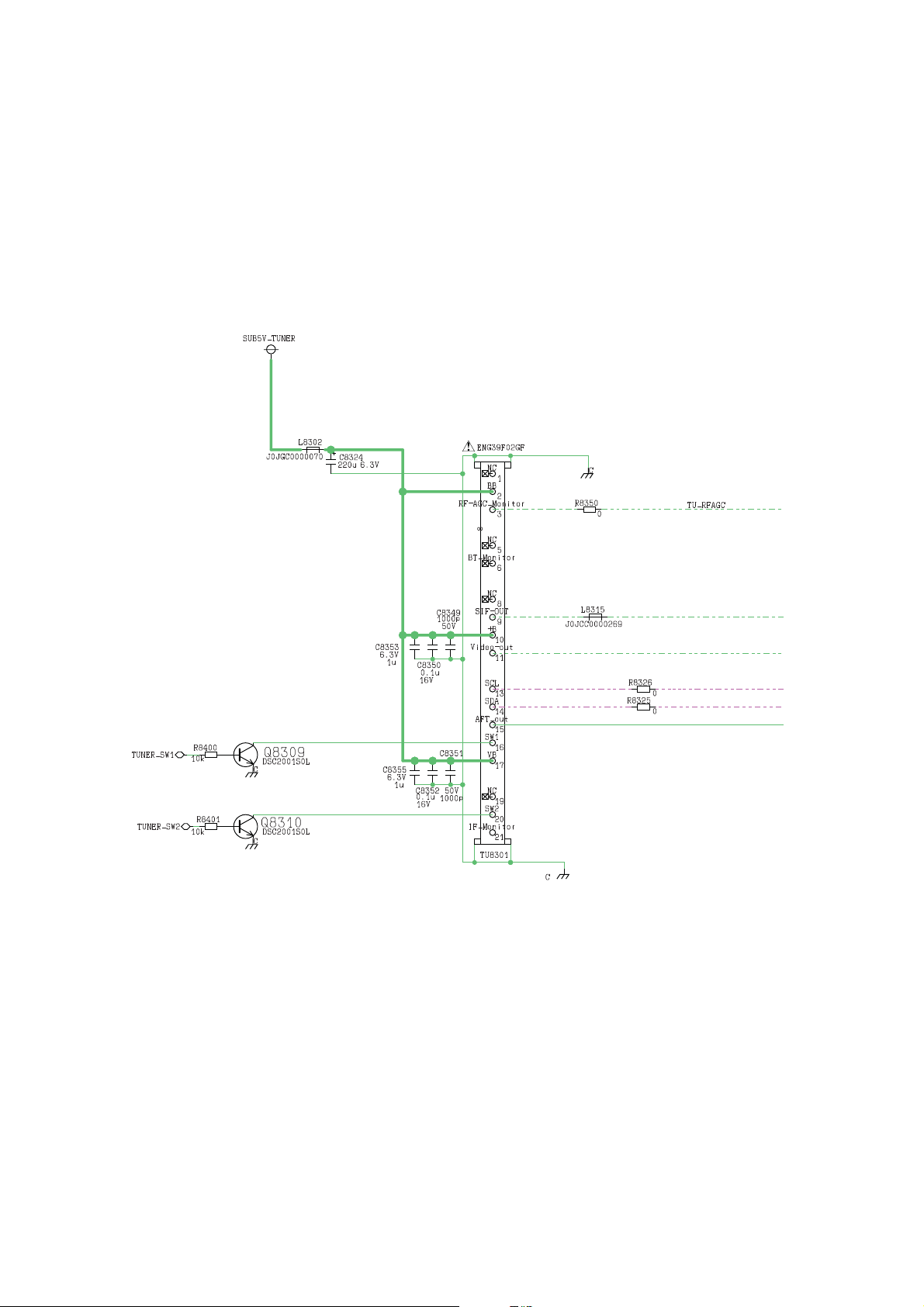
11.2.25. A Board - Sheet : 012 (1 / 3)
<1A>
<2A>
<3A>
<4A>
TH-L32A20X
65
Page 66
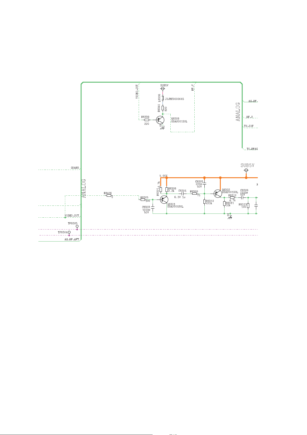
TH-L32A20X
<1B>
<2B>
<3B>
<1A>
<2A>
<3A>
<4A>
11.2.26. A Board - Sheet : 012 (2 / 3)
66
Page 67
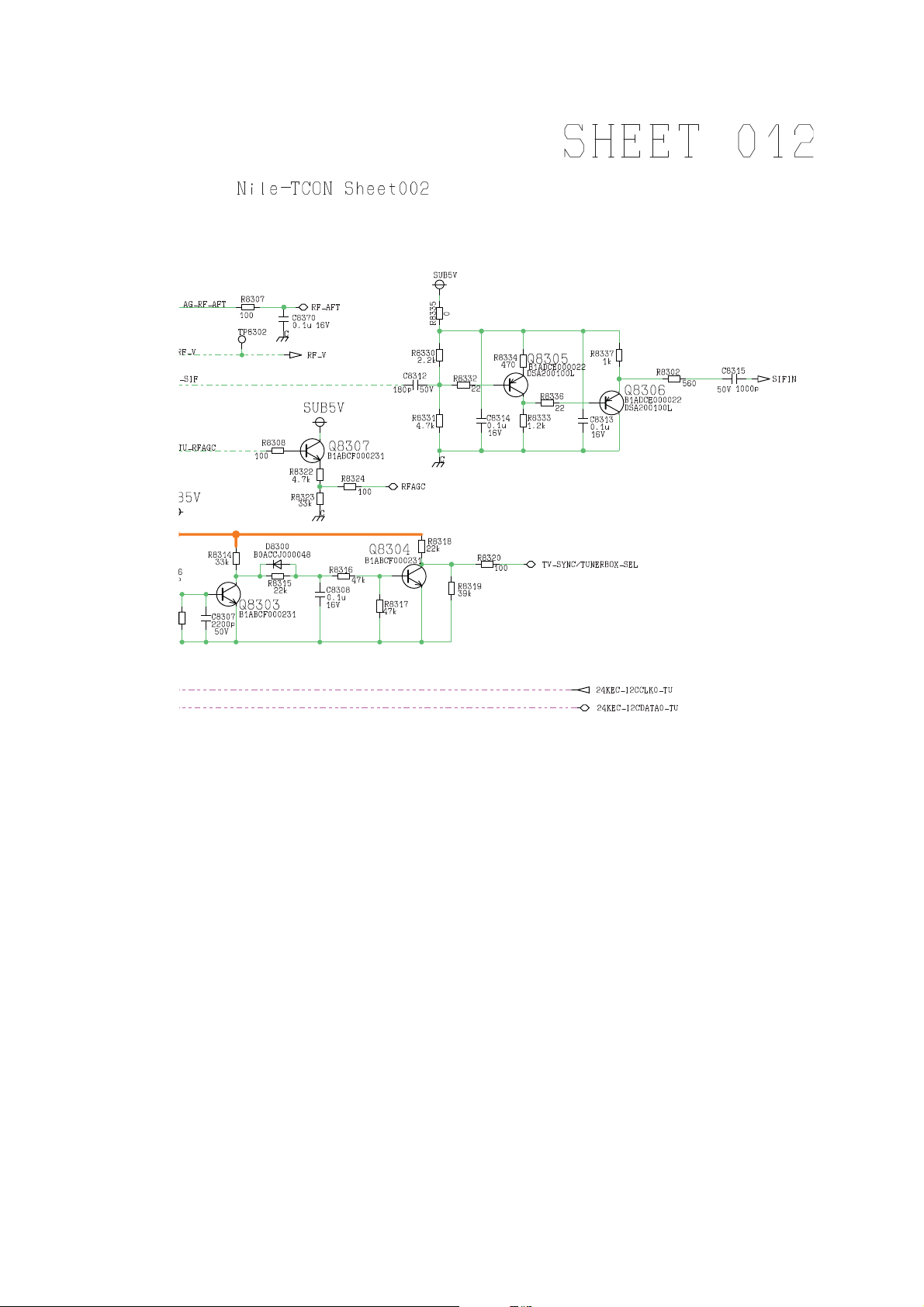
11.2.27. A Board - Sheet : 012 (3 / 3)
<1B>
<2B>
<3B>
TH-L32A20X
67
Page 68
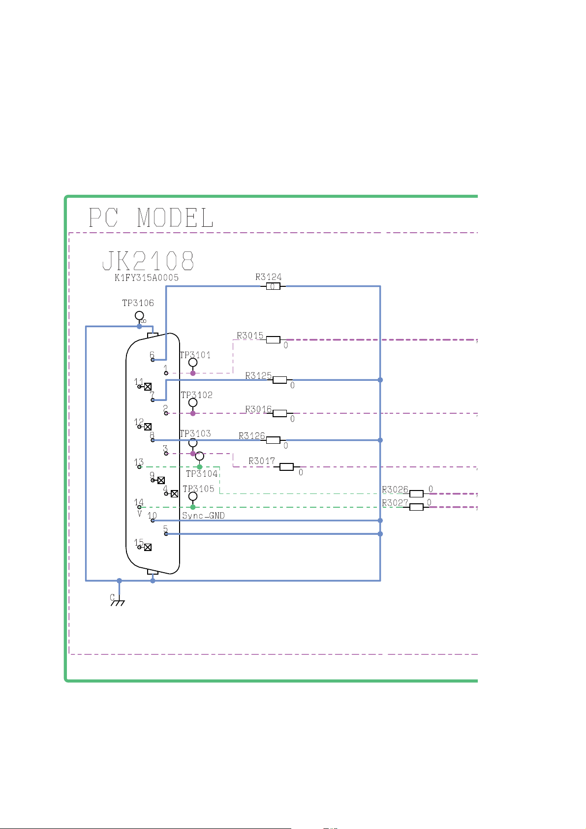
TH-L32A20X
11.2.28. A Board - Sheet : 015 (1 / 4)
<1A>
<2A>
<3A>
68
<4A>
Page 69
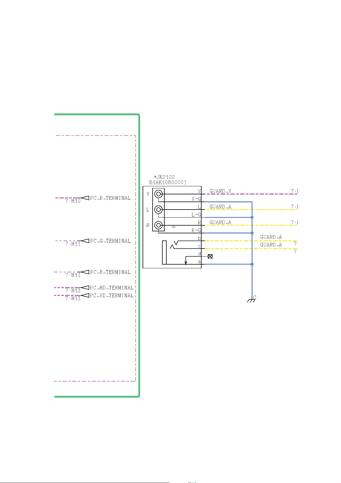
11.2.29. A Board - Sheet : 015 (2 / 4)
<1B>
<2B>
<3B>
<1A>
<2A>
<3A>
<4A>
TH-L32A20X
69
Page 70
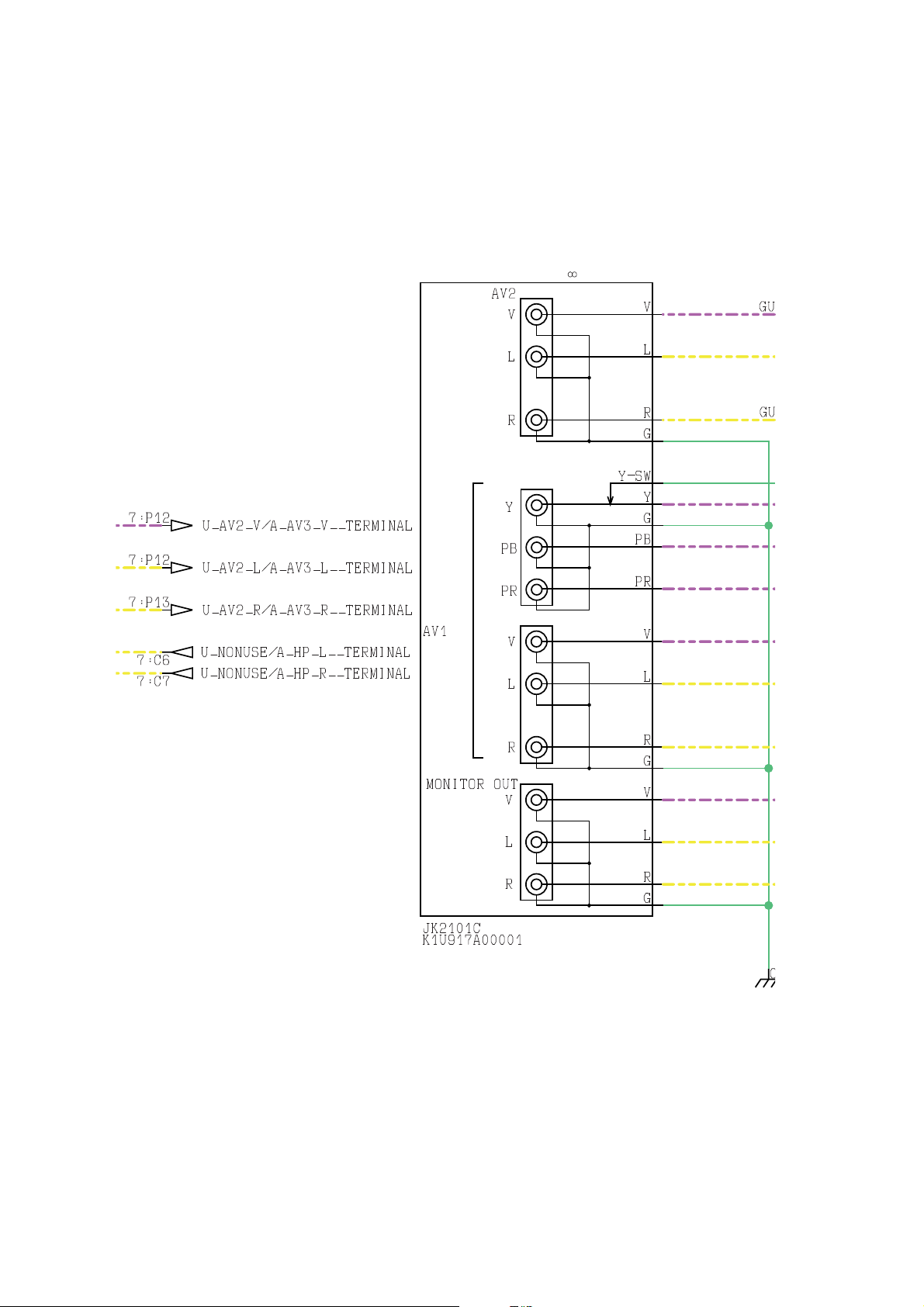
TH-L32A20X
<1C>
<2C>
<3C>
<4C>
<5C>
<1B>
<2B>
<3B>
11.2.30. A Board - Sheet : 015 (3 / 4)
70
Page 71
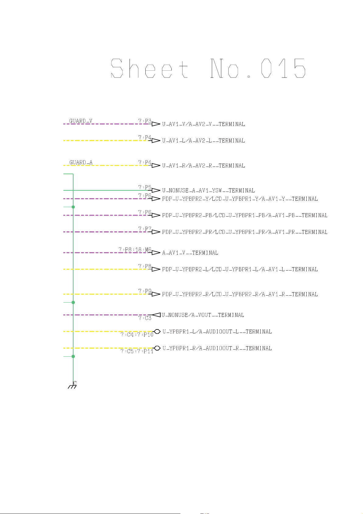
11.2.31. A Board - Sheet : 015 (4 / 4)
<1C>
<2C>
<3C>
<4C>
<5C>
TH-L32A20X
71
Page 72
TH-L32A20X
<1A>
<2A>
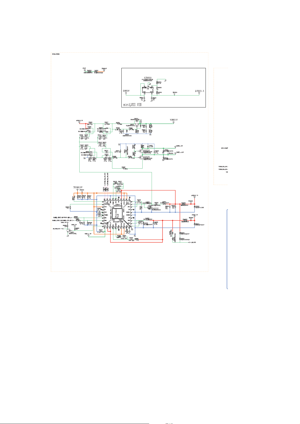
11.2.32. A Board - Sheet : 016 (1 / 4)
72
Page 73
<1B>
<2B>
<3B>
<4B>
<1A>
<2A>
TH-L32A20X
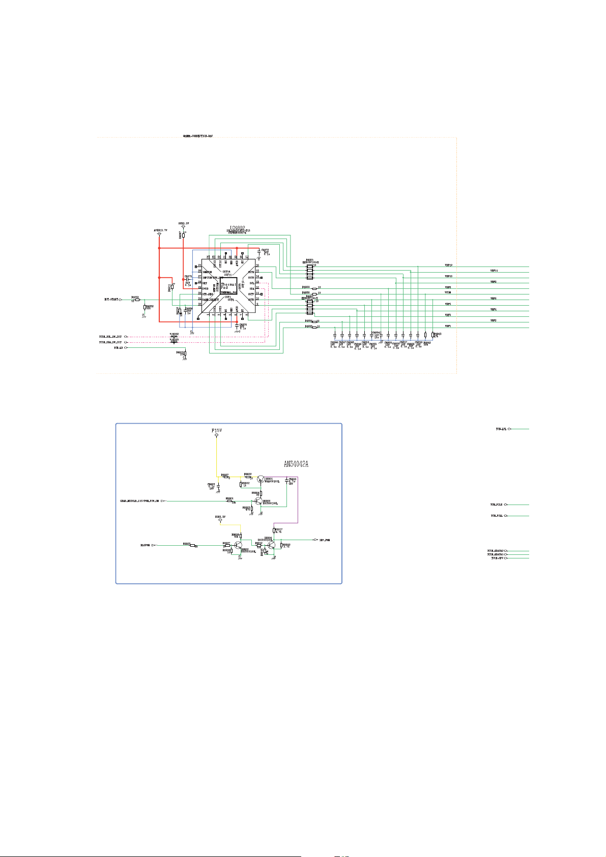
11.2.33. A Board - Sheet : 016 (2 / 4)
73
Page 74
TH-L32A20X
<1C>
<2C>
<3C>
<4C>
<5C>
<6C>
<1B>
<2B>
<3B>
<4B>
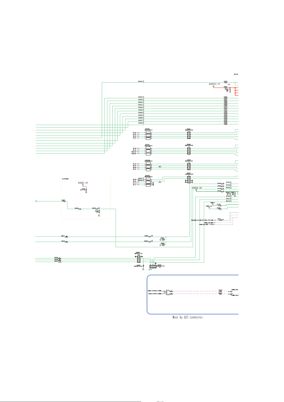
11.2.34. A Board - Sheet : 016 (3 / 4)
74
Page 75
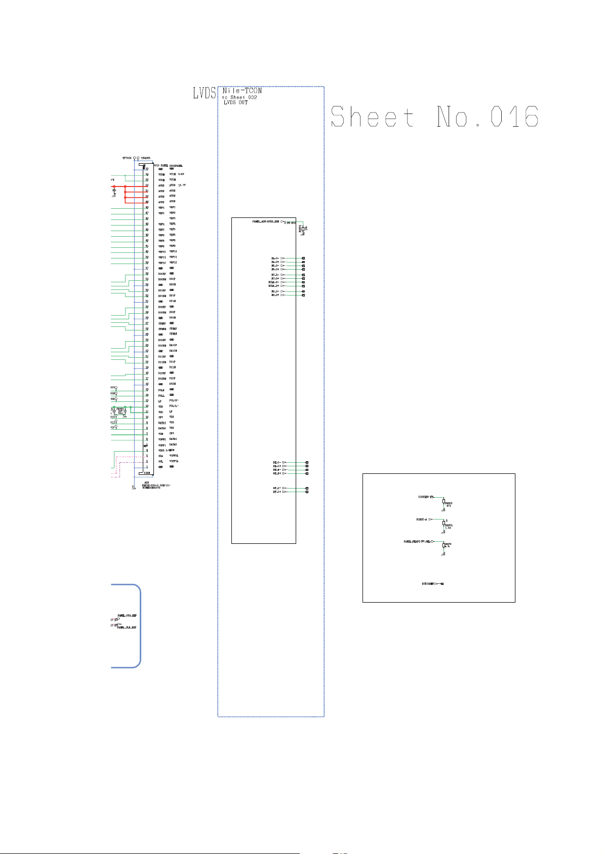
11.2.35. A Board - Sheet : 016 (4 / 4)
<1C>
<2C>
<3C>
<4C>
<5C>
<6C>
TH-L32A20X
75
Page 76
TH-L32A20X
<1A>
<2A>
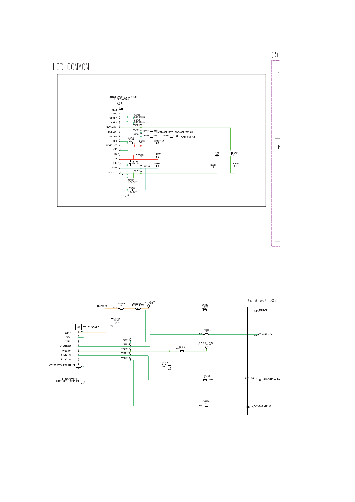
11.2.36. A Board - Sheet : 017 (1 / 4)
76
Page 77
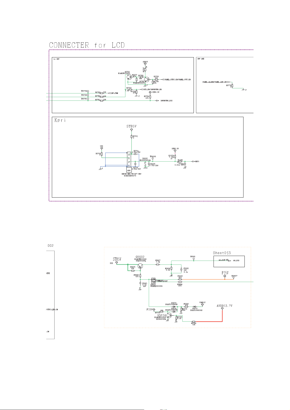
<1B>
<2B>
<3B>
<4B>
<1A>
<2A>
TH-L32A20X
11.2.37. A Board - Sheet : 017 (2 / 4)
77
Page 78
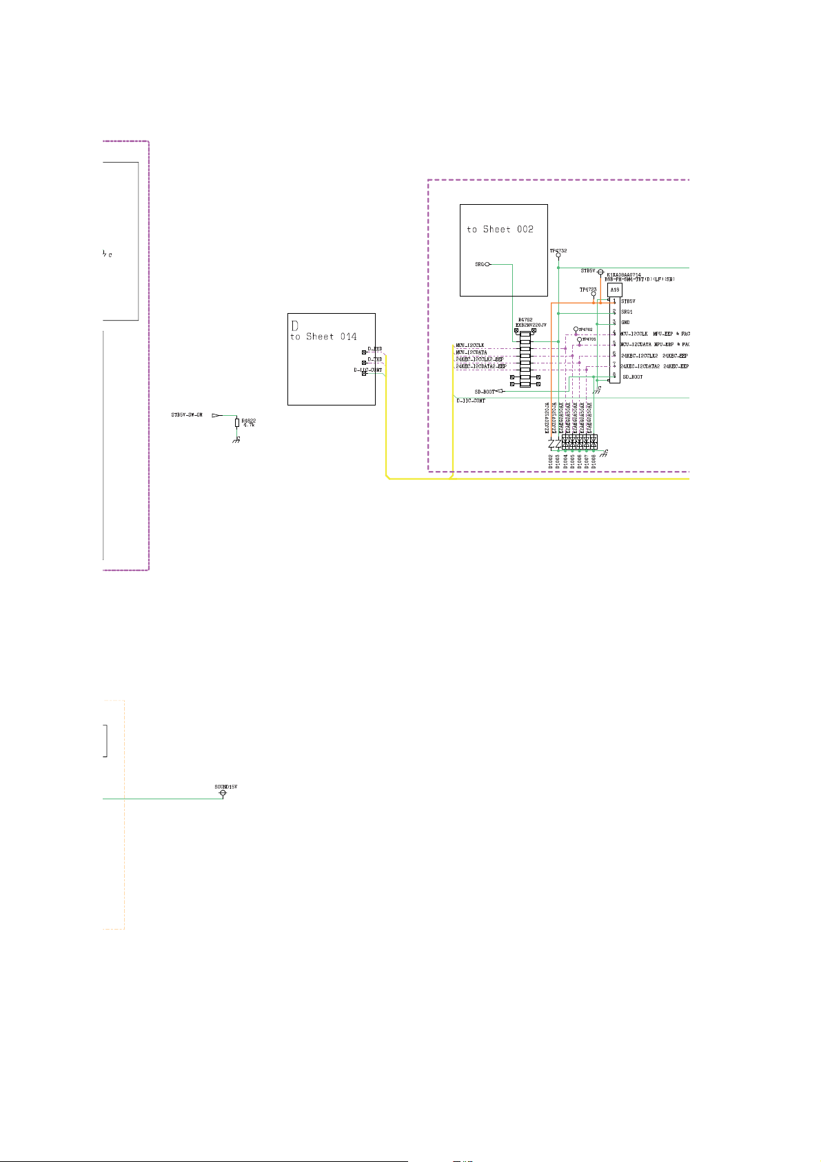
TH-L32A20X
<1C>
<2C>
<3C>
<4C>
<1B>
<2B>
<3B>
<4B>
11.2.38. A Board - Sheet : 017 (3 / 4)
78
Page 79
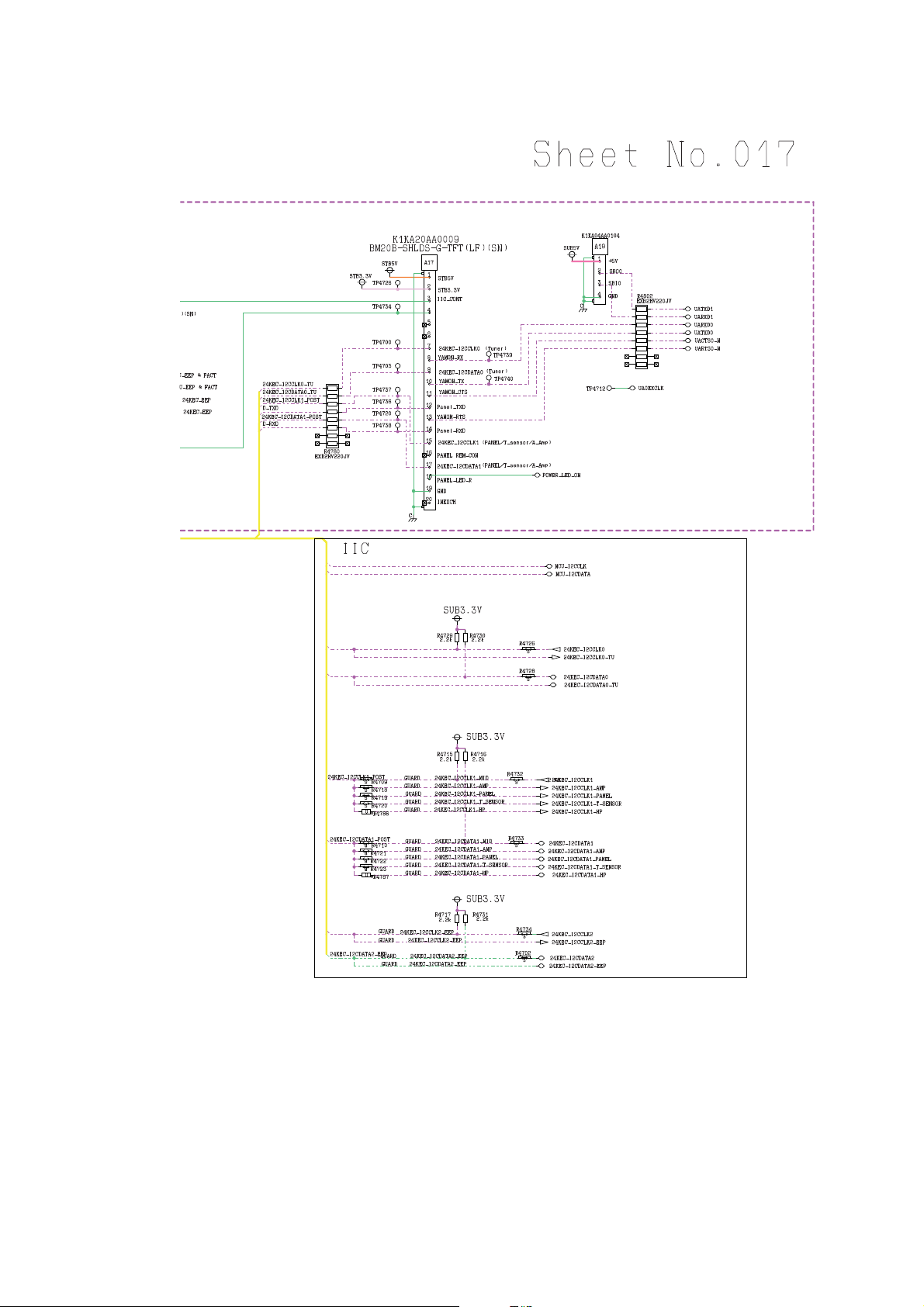
<1C>
<2C>
<3C>
<4C>
TH-L32A20X
11.2.39. A Board - Sheet : 017 (4 / 4)
79
Page 80
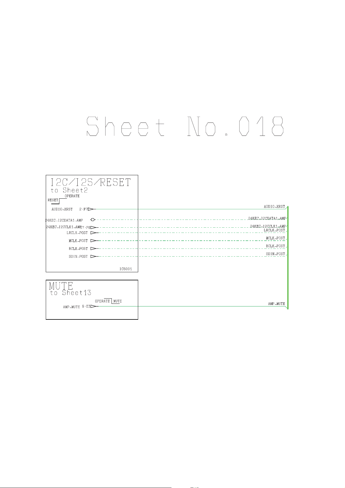
TH-L32A20X
11.2.40. A Board - Sheet : 018 (1 / 1)
80
Page 81
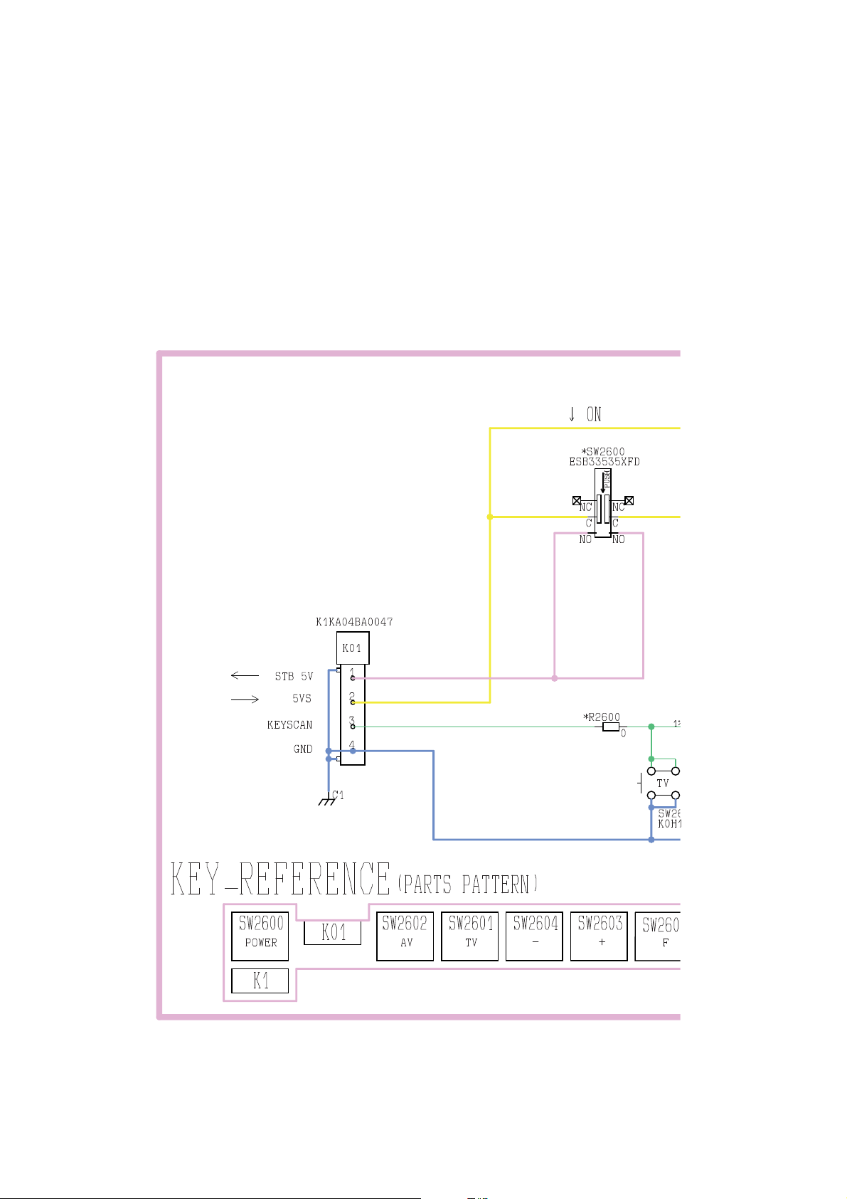
11.3. K Board
<1A>
<2A>
<3A>
<4A>
11.3.1. K Board (1 / 2)
TH-L32A20X
81
Page 82
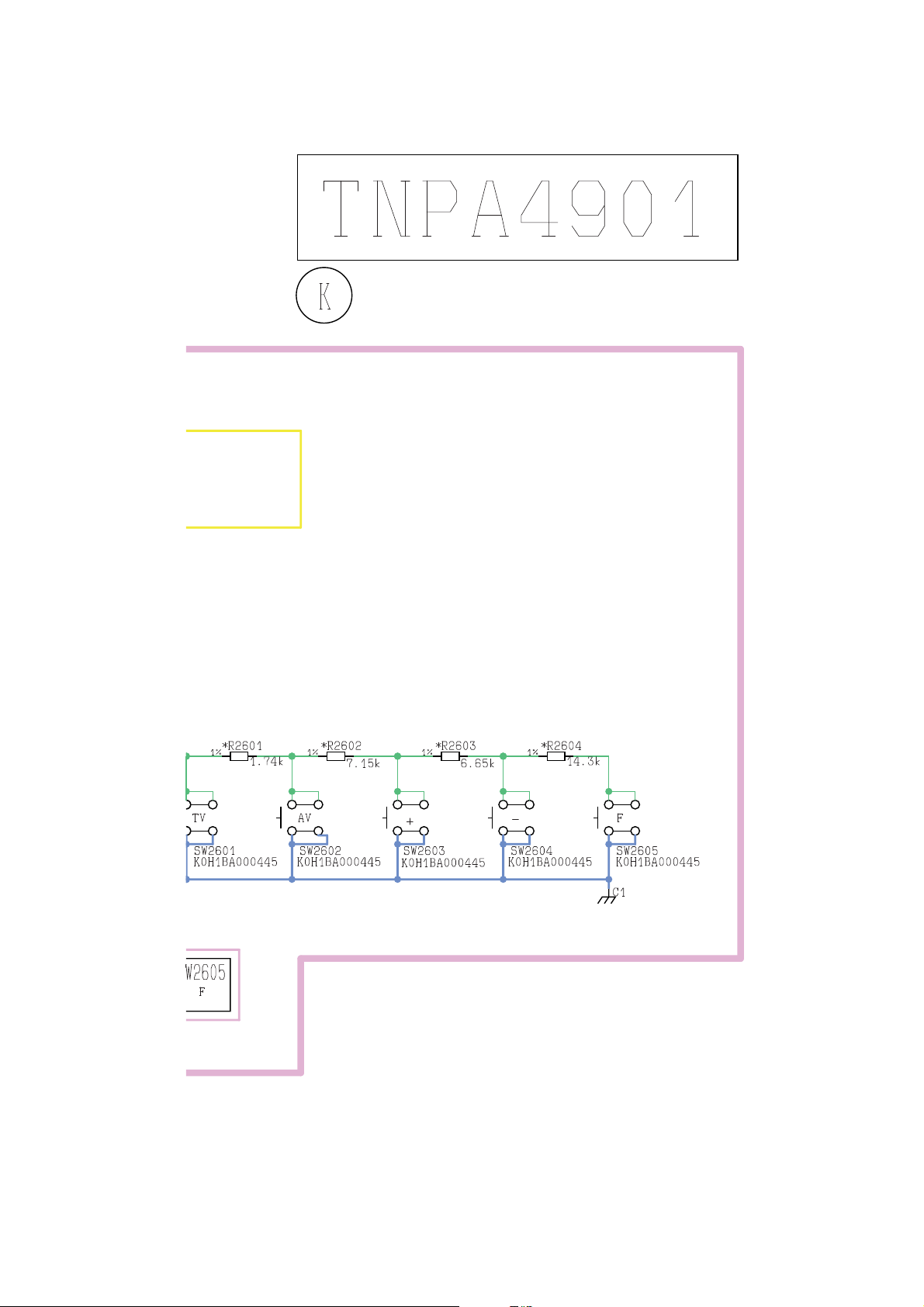
TH-L32A20X
<1A>
<2A>
<3A>
<4A>
11.3.2. K Board (2 / 2)
82
Page 83
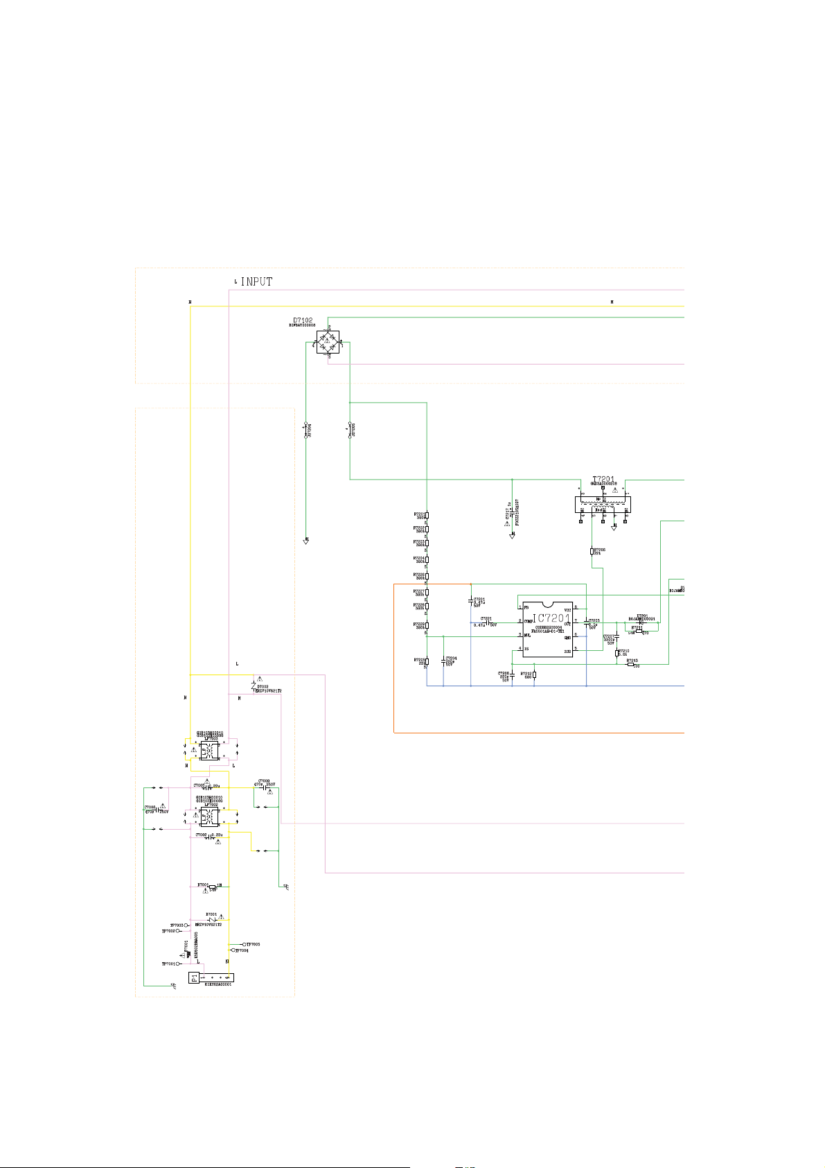
11.4. P Board
<1A>
<2A>
<3A>
<4A>
<5A>
<6A>
<7A>
11.4.1. P Board (1 / 5)
TH-L32A20X
83
Page 84
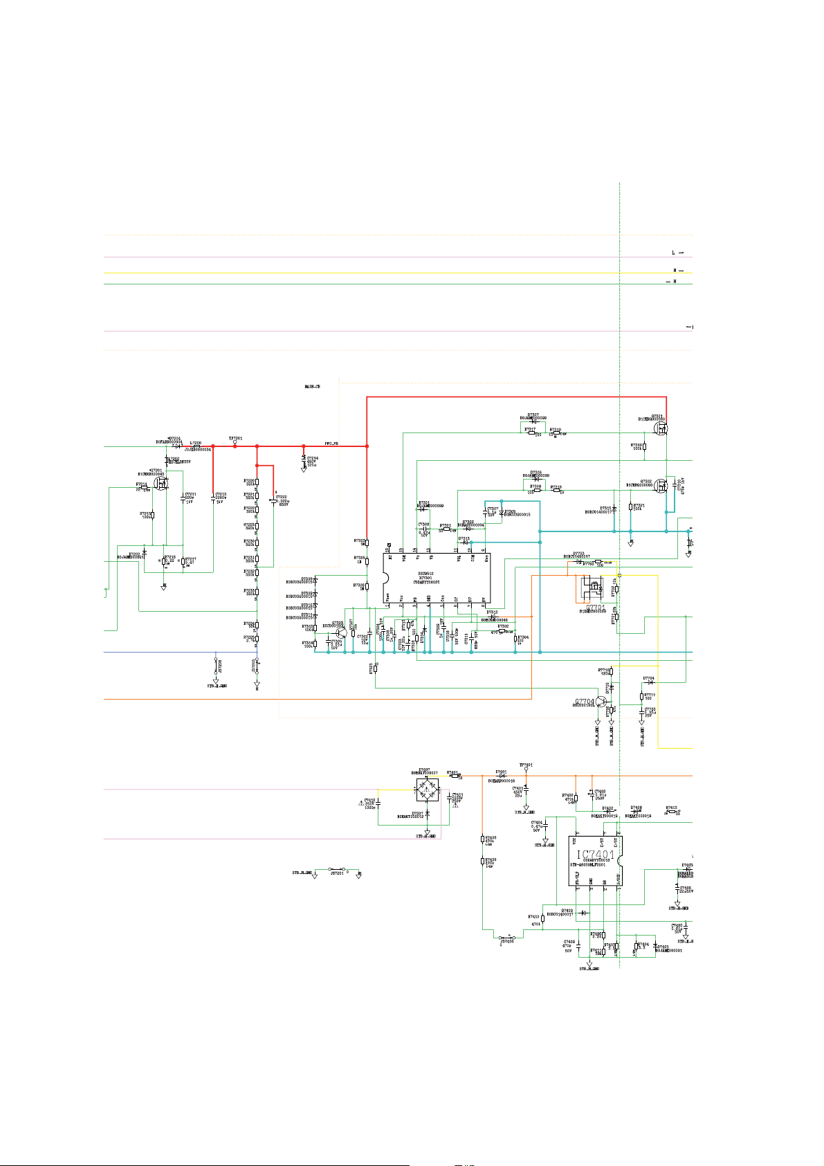
TH-L32A20X
<1B>
<2B>
<3B>
<4B>
<5B>
<6B>
<1A>
<2A>
<3A>
<4A>
<5A>
<6A>
<7A>
11.4.2. P Board (2 / 5)
84
Page 85
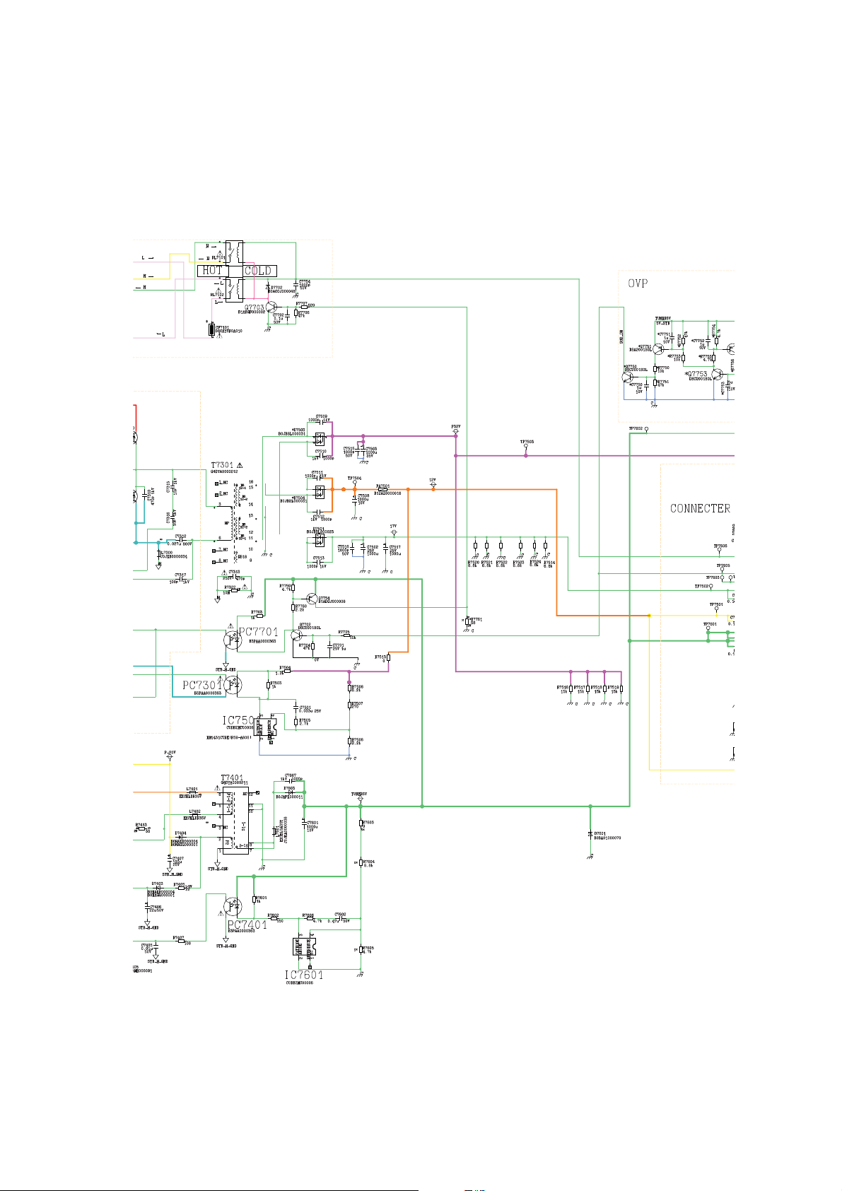
<1C>
<2C>
<3C>
<1B>
<2B>
<3B>
<4B>
<5B>
<6B>
TH-L32A20X
11.4.3. P Board (3 / 5)
85
Page 86
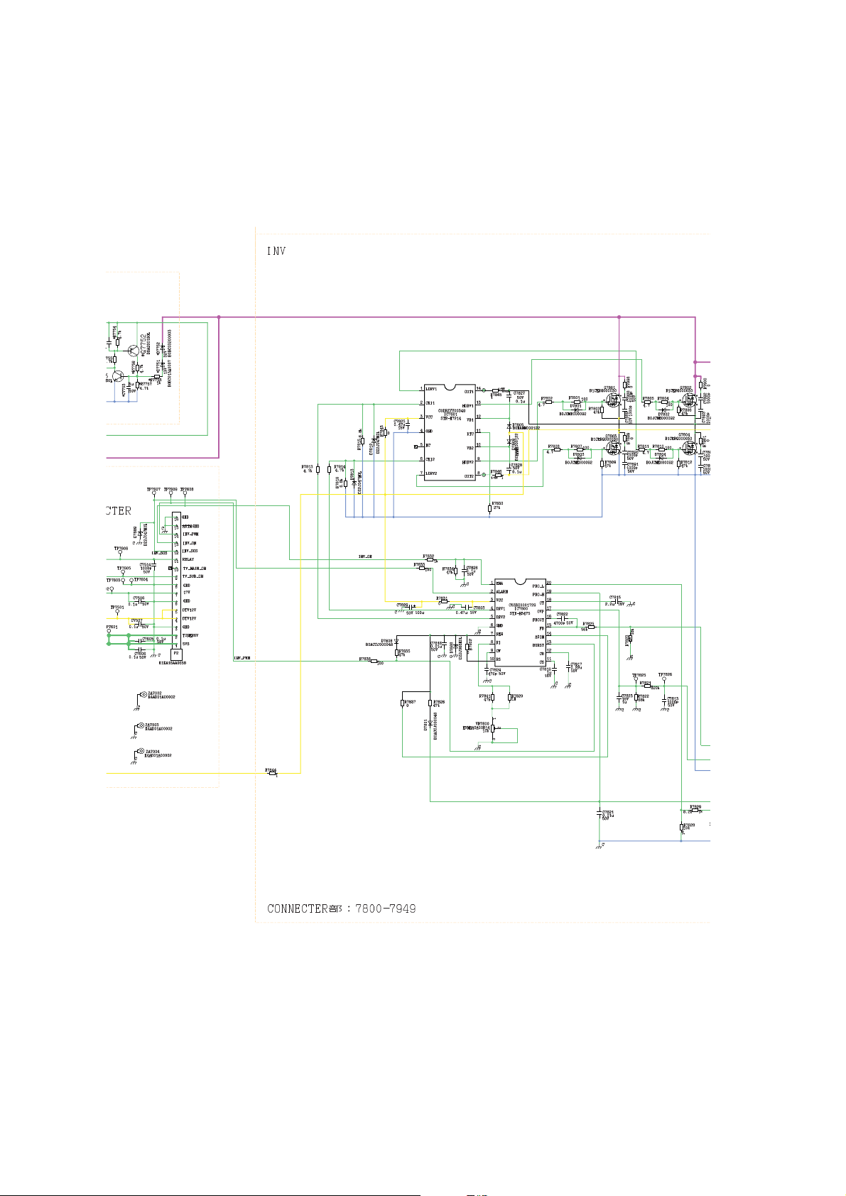
TH-L32A20X
11.4.4. P Board (4 / 5)
<1C>
<1D>
<2C>
<3C>
<2D>
<3D>
86
<4D>
Page 87
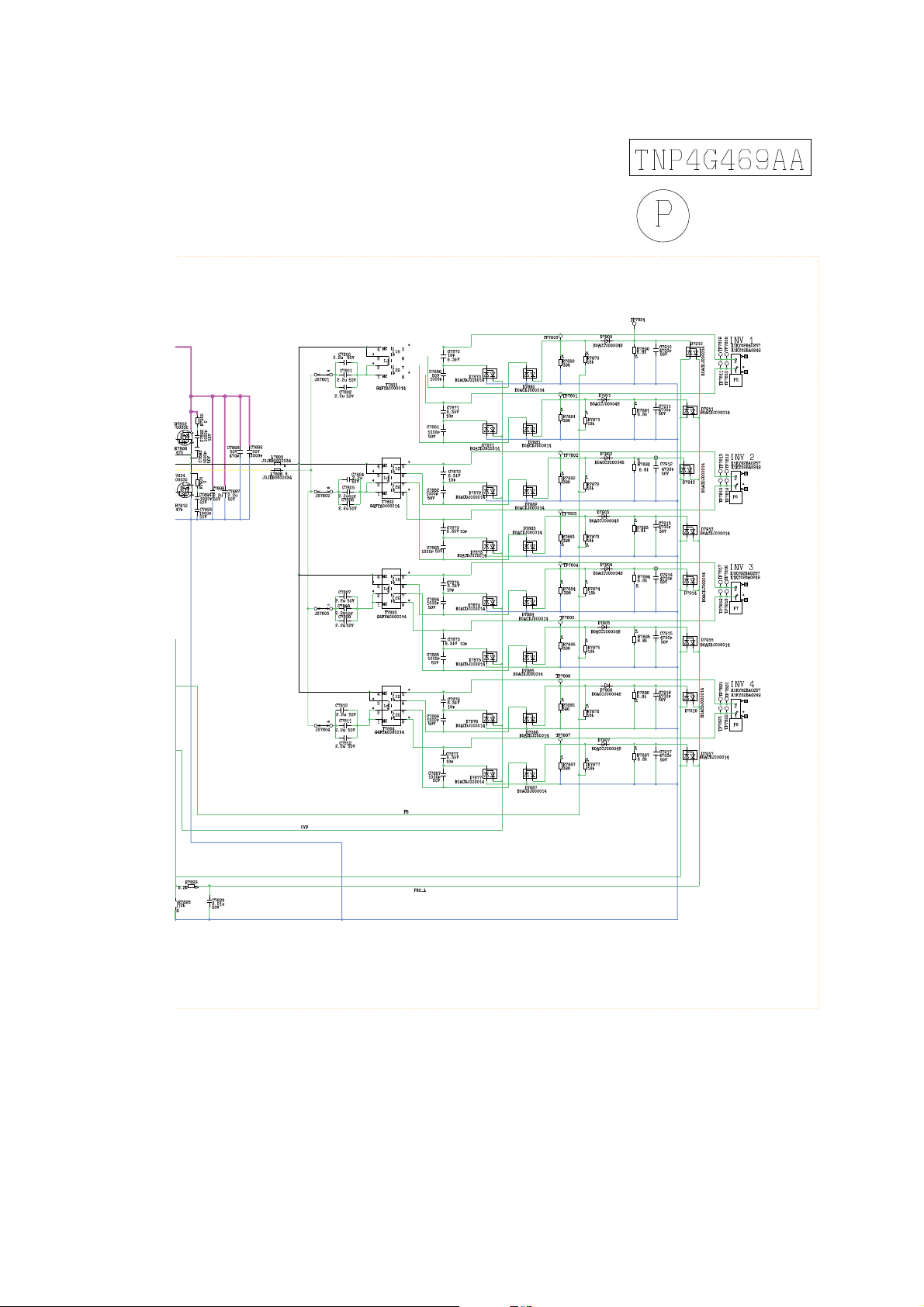
11.4.5. P Board (5 / 5)
<1D>
<2D>
TH-L32A20X
<3D>
<4D>
87
Page 88
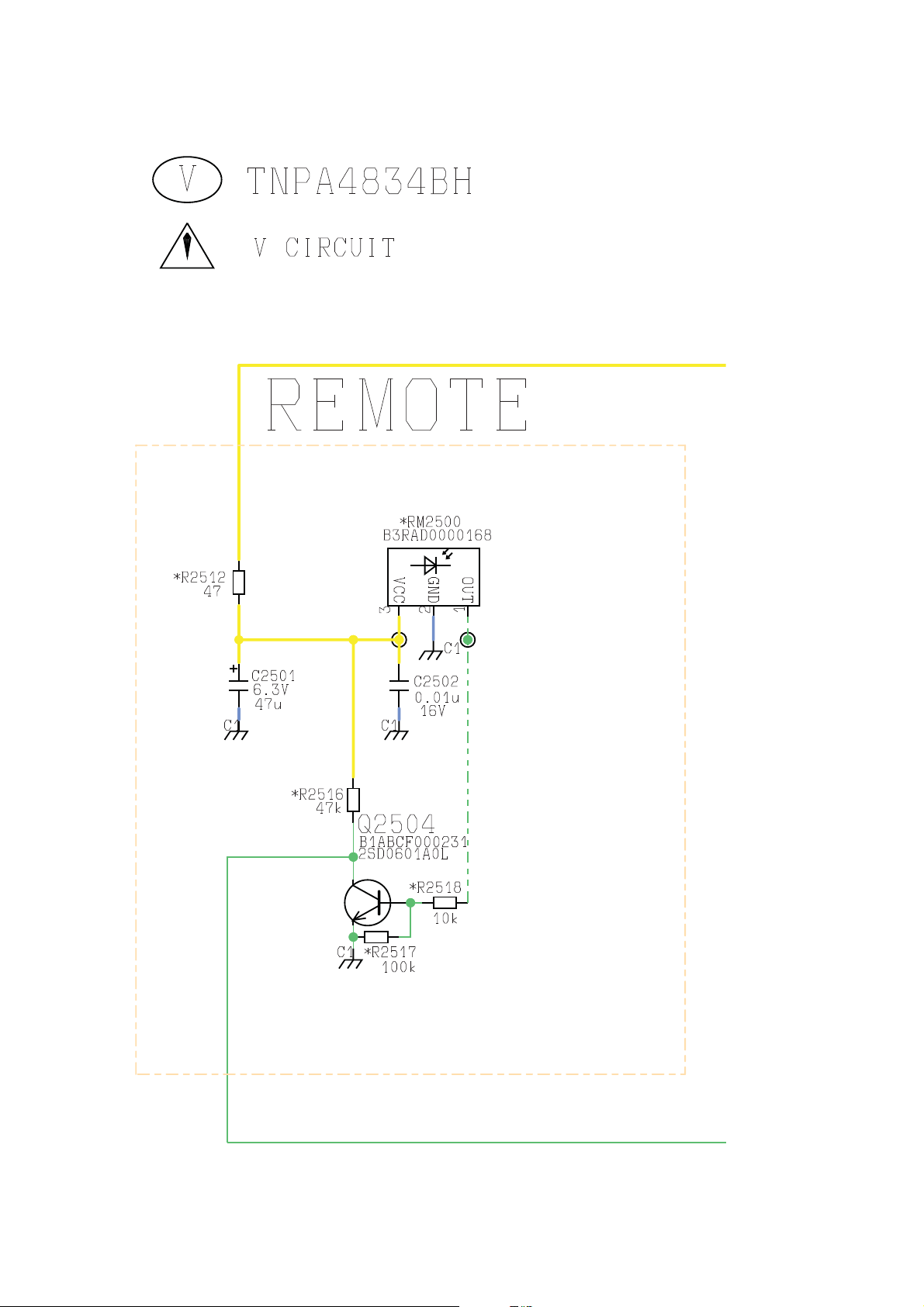
TH-L32A20X
<1A>
<2A>
11.5. V Board
11.5.1. V Board (1 / 3)
88
Page 89
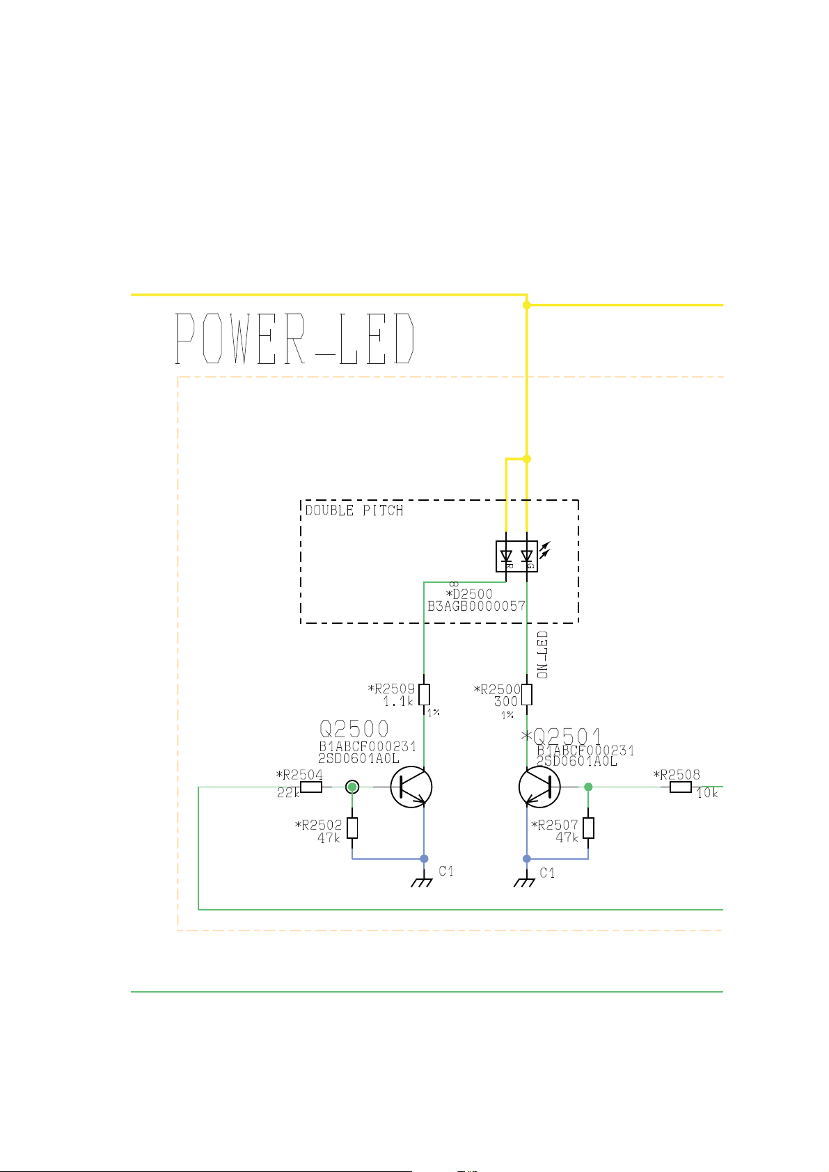
11.5.2. V Board (2 / 3)
<1B>
<2B>
<4B>
<3B>
<1A>
<2A>
TH-L32A20X
89
Page 90
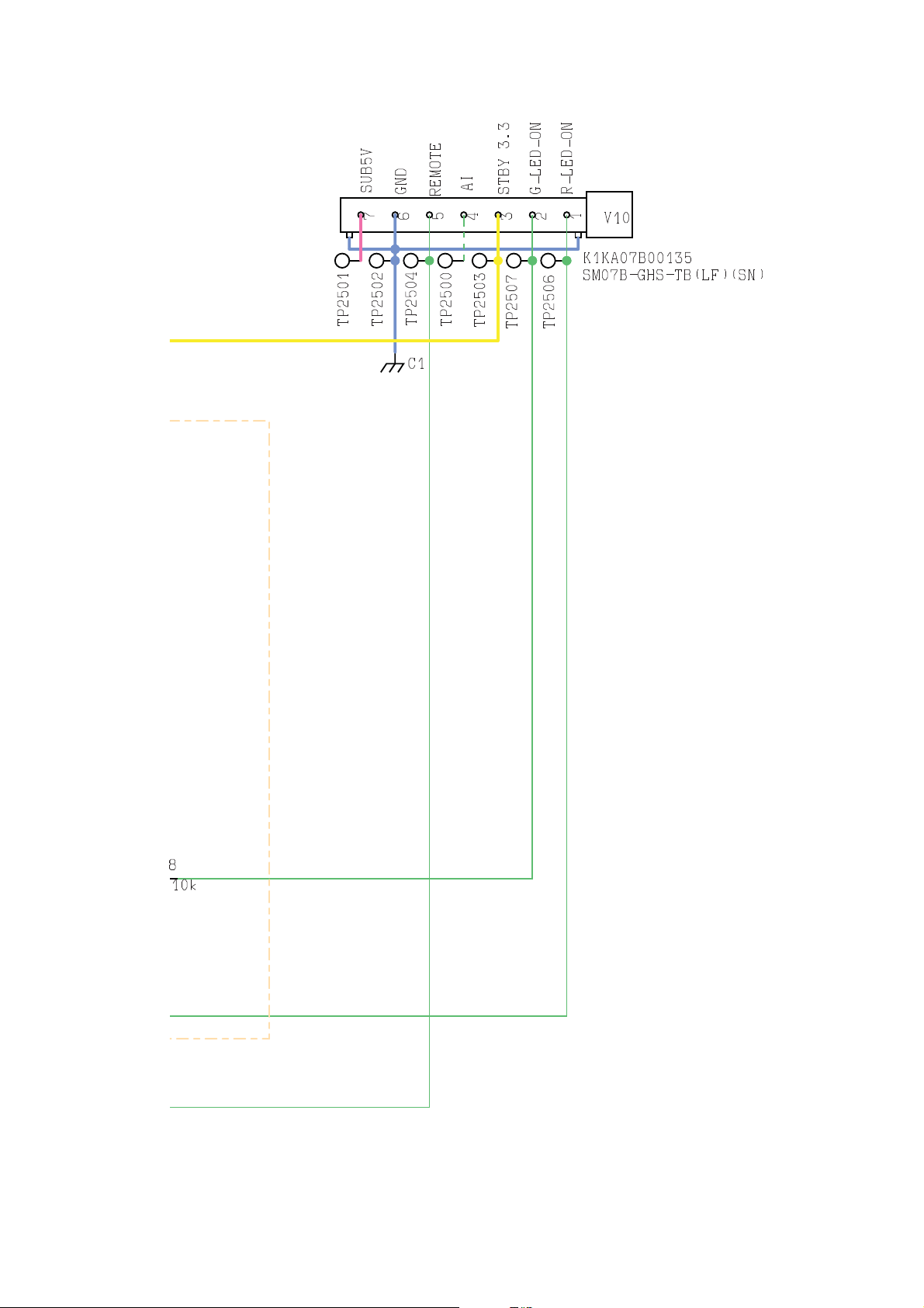
TH-L32A20X
<1B>
<2B>
<4B>
<3B>
11.5.3. V Board (3 / 3)
90
Page 91
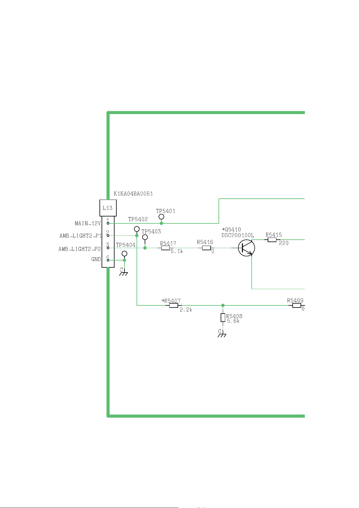
11.6. L Board
<1A>
<2A>
<3A>
11.6.1. L Board (1 / 2)
TH-L32A20X
91
Page 92
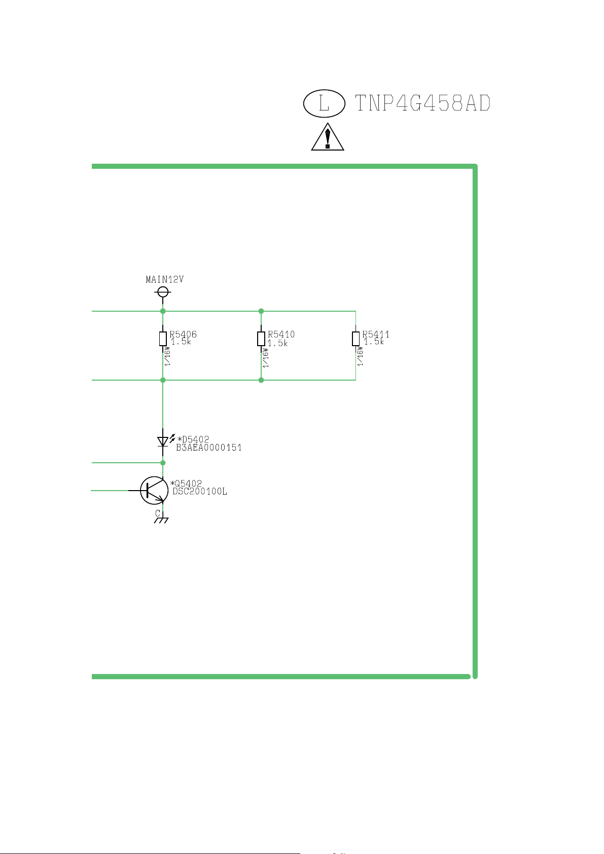
TH-L32A20X
<1A>
<2A>
<3A>
11.6.2. L Board (2 / 2)
92
Page 93
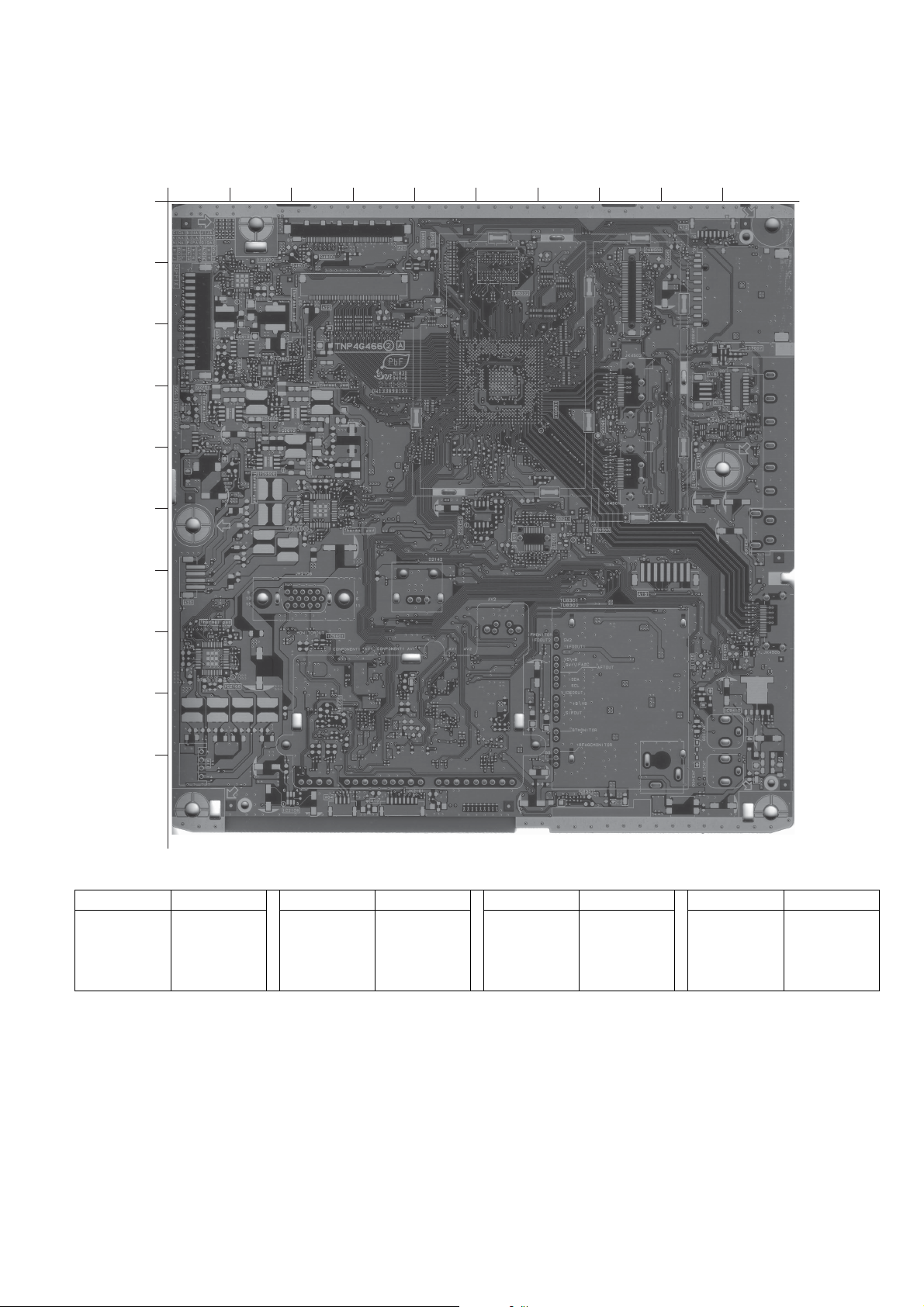
12 Printed Circuit Board
1
A
B
C
D
E
F
G
H
I
J
2 3 4 5 6 7 8 9 10
12.1. A-Board
A-Board (A Side)
TNP4G466
TH-L32A20X
Parts Location
Ref. No Location Ref. No Location Ref. No Location Ref. No Location
IC2106 H2 IC3202 F5 IC5601 H3 IC5610 D2
IC2108 J3 IC4800 B2 IC5606 D2 IC8001 D7
IC2501 F3 IC4802 C2 IC5607 C10 IC8002 B6
IC3200 F8 IC5410 I10 IC5608 E2
93
Page 94
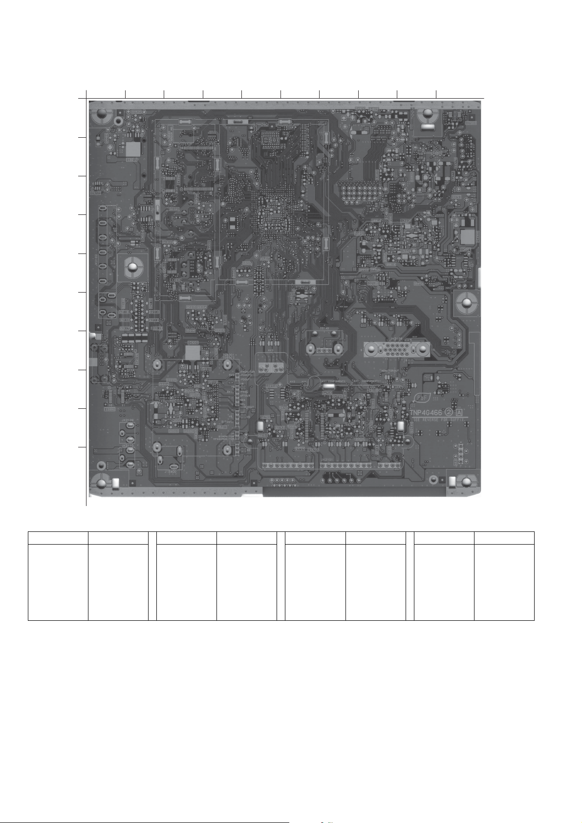
TH-L32A20X
1
A
B
C
D
E
F
G
H
I
J
2 3 4 5 6 7 8 9 10
12.2. A-Board
A-Board (B Side)
TNP4G466
Parts Location
Ref. No Location Ref. No Location Ref. No Location Ref. No Location
IC2105 E8 IC3390 C3 IC4803 B9 IC8004 C8
IC2109 G2 IC4600 E3 IC4804 C8 IC8300 I3
IC2110 H8 IC4601 E3 IC5605 D9 IC8301 D10
IC2300 D10 IC4700 J6 IC5609 D9 IC8502 A3
IC3201 G3 IC4701 C1 IC5613 B2 IC8503 H5
IC3350 H1 IC4702 I8 IC7000 A10 IC8850 F6
94
Page 95
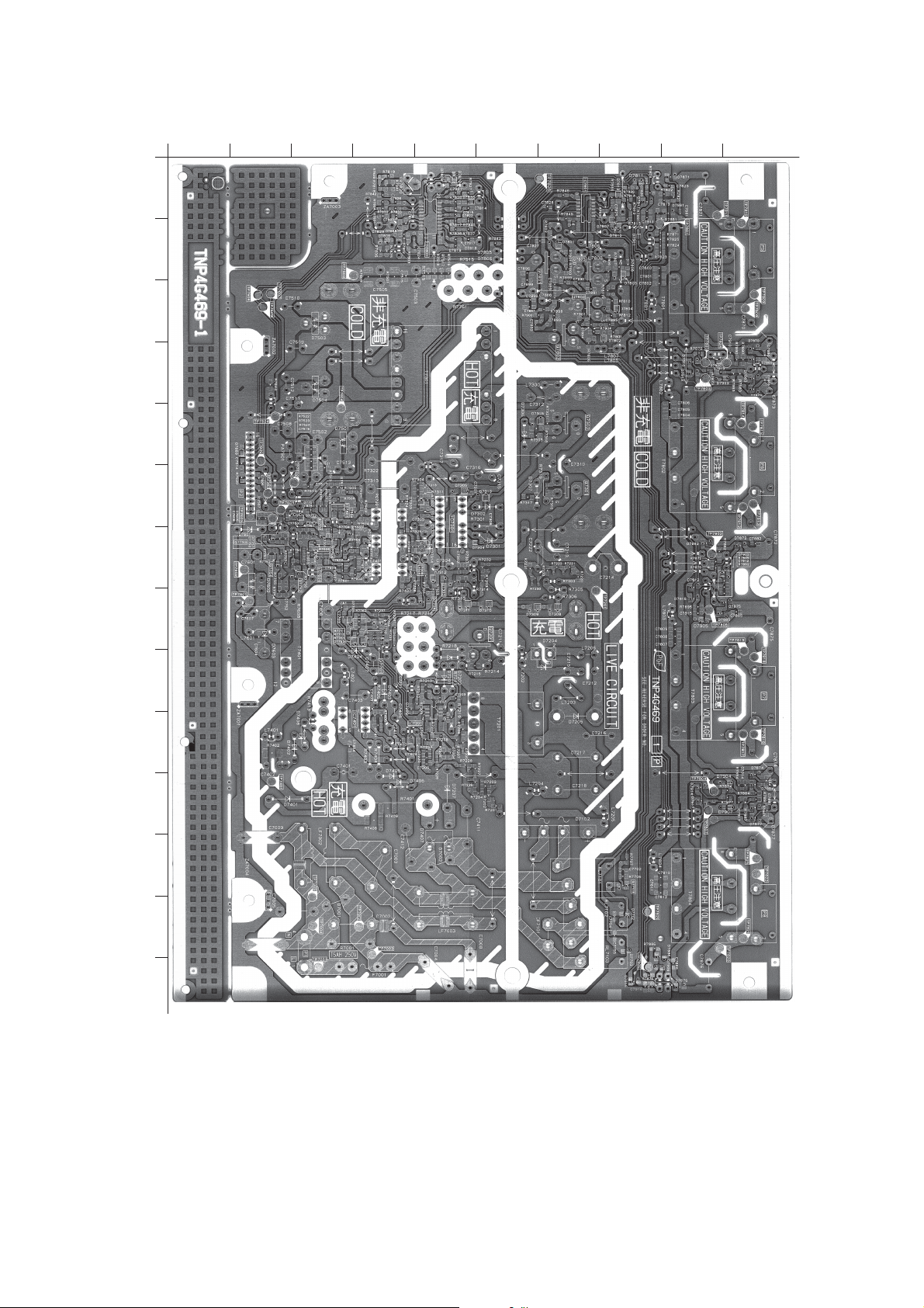
12.3. P-Board
1
A
B
C
D
E
F
G
H
I
K
L
M
N
J
2 3 4 5 6 7 8 9 10
P-Board (A Side)
TNP4G469
TH-L32A20X
95
Page 96
TH-L32A20X
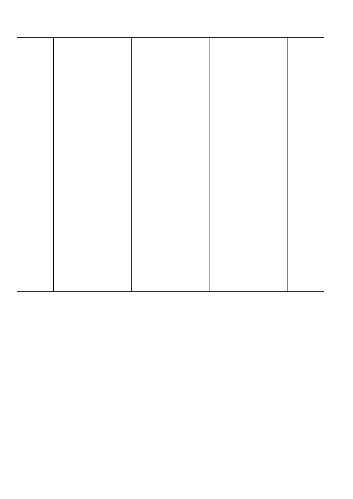
Parts Location
Ref. No Location Ref. No Location Ref. No Location Ref. No Location
IC7201 J4 D7001 M3 D7501 E3 D7873 E10
IC7301 G5 D7002 L5 D7503 D3 D7874 K10
IC7401 J3 D7102 L7 D7504 E3 D7875 H10
IC7501 F3 D7201 I5 D7601 G2 D7876 N9
IC7601 G3 D7202 I5 D7602 H2 D7877 L10
IC7800 B5 D7204 I7 D7603 I2 D7880 D10
IC7801 A7 D7205 J7 D7701 G3 D7881 A9
D7207 K5 D7702 M8 D7882 G9
D7301 G6 D7703 N8 D7883 D10
D7302 G5 D7704 H4 D7884 K10
D7303 F4 D7705 H3 D7885 H9
D7304 G5 D7751 E3 D7886 N8
D7305 F5 D7752 G3 D7887 K10
D7306 E6 D7753 I3 D7888 B4
D7307 F6 D7801 B7 D7889 E1
D7308 H7 D7802 D8 D7900 D9
D7309 H6 D7803 C8 D7901 B8
D7310 H6 D7804 C8 D7902 G10
D7311 H5 D7805 B6 D7903 D9
D7312 G5 D7807 B7 D7904 K9
D7313 F6 D7808 B4 D7905 H9
D7314 G5 D7809 A5 D7906 N8
D7315 E6 D7810 A5 D7907 K9
D7401 K2 D7811 A8 D7910 D9
D7402 J2 D7812 B8 D7911 A8
D7403 I4 D7813 A8 D7912 H9
D7404 I3 D7833 A5 D7913 D9
D7405 K4 D7704 H4 D7914 K9
D7406 K4 D7705 H3 D7915 H9
D7407 L4 D7870 D10 D7916 H8
D7408 J2 D7871 A9 D7917 K9
D7409 J4 D7872 G10
96
Page 97
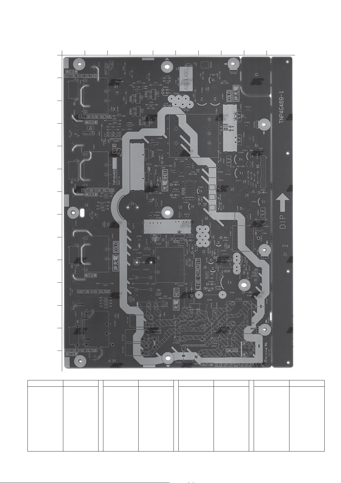
12.4. P-Board
1
A
B
C
D
E
F
G
H
I
K
L
M
N
J
2 3 4 5 6 7 8 9 10
P-Board (B Side)
TNP4G469
TH-L32A20X
Ref. No Location Ref. No Location Ref. No Location Ref. No Location
IC7301 G6 D7001 M7 D7306 I9 D7408 J8
IC7401 K9 D7002 L6 D7307 F5 D7501 E7
D7102 L5 D7314 G6 D7503 C8
D7201 I6 D7401 K9 D7504 D8
D7202 I6 D7402 J8 D7601 G9
D7204 I5 D7403 I7 D7602 H9
D7205 J4 D7404 I7 D7603 I9
D7207 K6 D7405 K7 D7805 B5
D7301 G5 D7406 K7 D7806 B5
D7302 F5 D7407 K6
Parts Location
97
Page 98
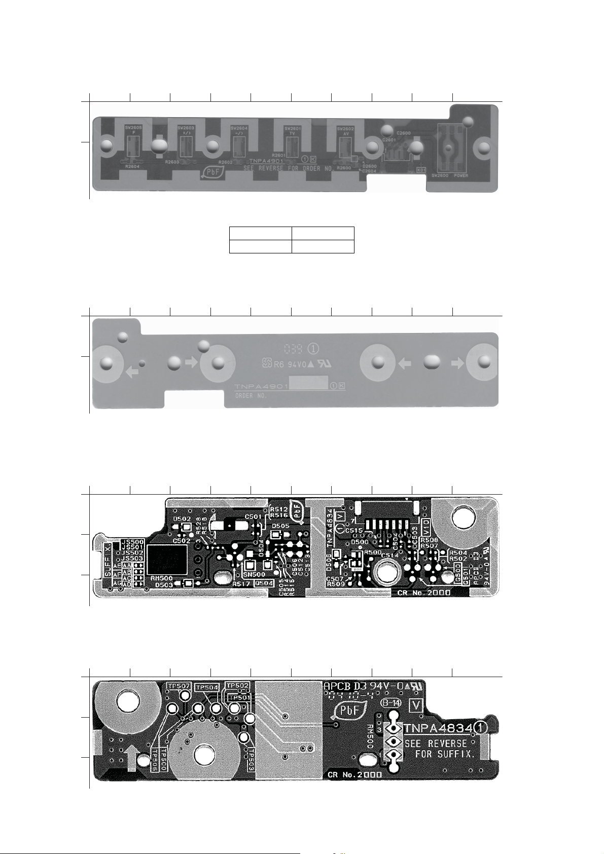
TH-L32A20X
1
A
B
2 3 4 5 6 7 8 9 10
1
A
B
2 3 4 5 6 7 8 9 10
1
A
B
C
2 3 4 5 6 7 8 9 10
1
A
B
C
2 3 4 5 6 7 8 9 10
12.5. K-Board
K-Board (A Side)
TNPA4901
12.6. K-Board
K-Board (B Side)
TNPA4901
Parts Location
Ref. No Location
D2600 B7
12.7. V-Board
V-Board (A Side)
TNPA4834
12.8. V-Board
V-Board (B Side)
TNPA4834
98
Page 99
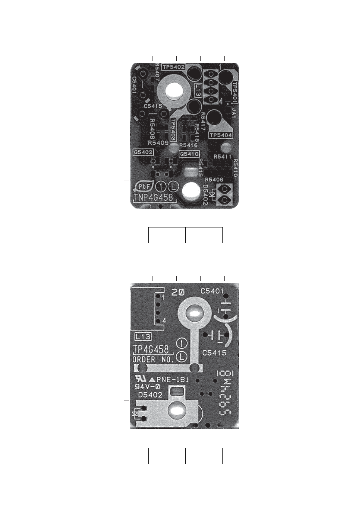
12.9. L-Board
L-Board (A Side)
TNP4G458
TH-L32A20X
1
A
B
C
D
E
F
2 3 4 5
Parts Location
Ref. No Location
D5402 F4
12.10. L-Board
L-Board (B Side)
TNP4G458
1
A
B
C
D
E
F
2 3 4 5
Parts Location
Ref. No Location
D5402 F1
99
Page 100
TH-L32A20X
13 Exploded View and Replacement Parts List
13.1. Exploded View and Mechanical Replacement Parts List
Please click the radio button for "Diagrams ll/Parts List" on the menu bar.
13.2. Electrical Replacement Parts List
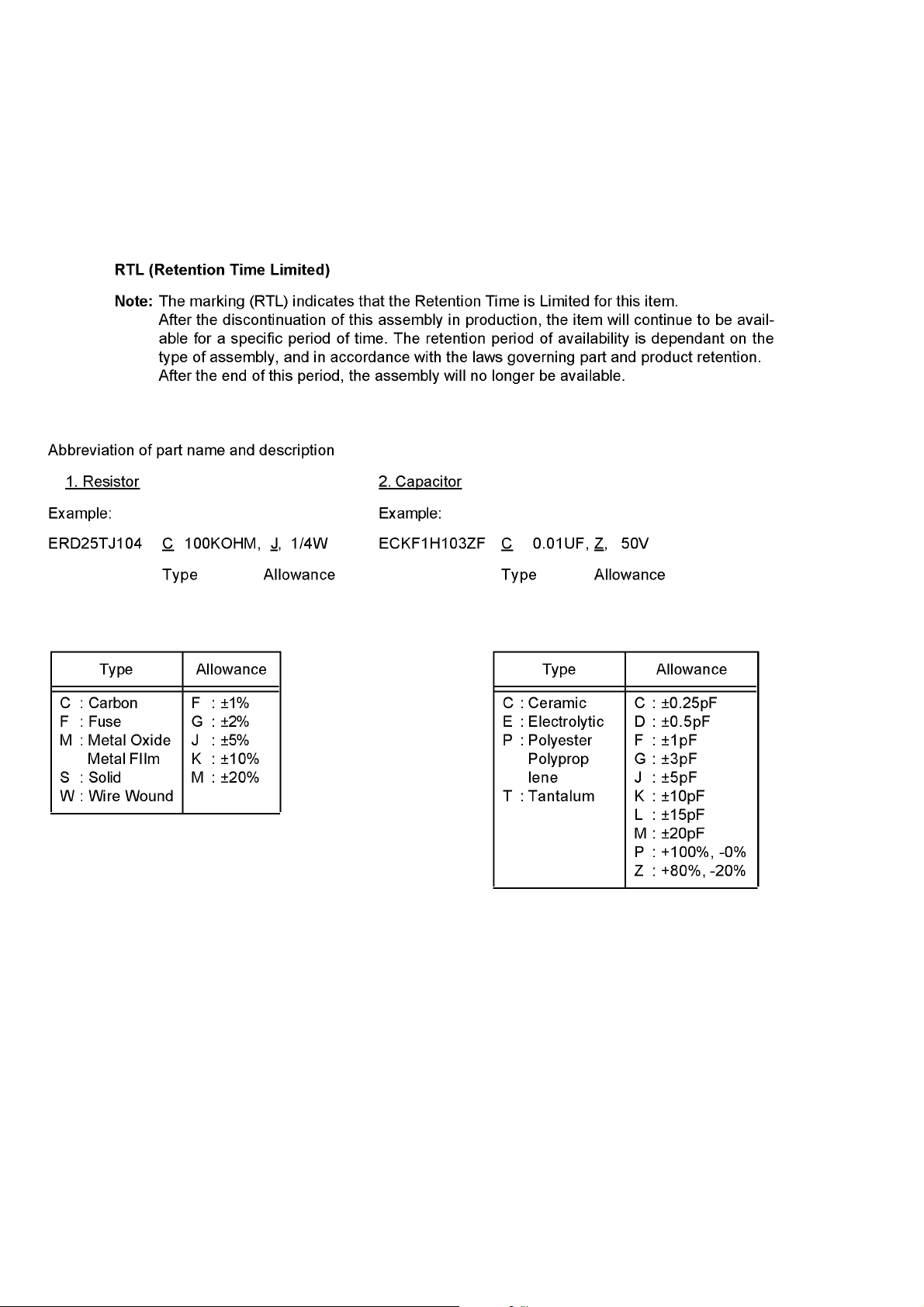
13.2.1. Replacement Parts List Notes
100
 Loading...