


Digital High Definition Plasma Television
TH-42PX50UA
TH-42PX500UA
Subject : Change P-board
Please file and use this manual together with the service manual for Model No
TH-42PX50U (Main), ORDER NO. ITD0503013CE
TH-42PX500U (Main), ORDER NO. MTNC050632C1
ORDER NO. ITD0510061SE
B19 Canada : B07
CONTENTS
Page Page
1 Parts Change Notice 2
1.1. Mechanical Replacement Parts List
1.2. Electrical Replacement Parts List
1.3. Interchangeability for CIRCUIT BOARD P
2 Note
2.1. TH-42PX50UA
2.2. TH-42PX500UA
3 Adjustment Procedure
3.1. Driver Set-up
3.2. Initialization Pulse Adjust
3.3. P.C.B. (Printed Circuit Board) exchange
3.4. Adjustment Volume Location
3.5. Test Point Location
4 Conductor Views
2
2
2
3
3
3
4
4
5
6
6
7
9
4.1. P-Board 9
5 Block and Schematic Diagrams
5.1. Schematic Diagram Notes
5.2. P-Board Block Diagram
5.3. P-Board (1 of 6) Schematic Diagram
5.4. P-Board (2 of 6) Schematic Diagram
5.5. P-Board (3 of 6) Schematic Diagram
5.6. P-Board (4 of 6) Schematic Diagram
5.7. P-Board (5 of 6) Schematic Diagram
5.8. P-Board (6 of 6) Schematic Diagram
6 Replacement Parts List (P-board)
6.1. Replacement Parts List Notes
6.2. Replacement Parts List (P-board)
7 Schematic Diagram for printing with A4
13
13
14
15
16
17
18
19
20
21
21
22
27
© 2005 Matsushita Electric Industrial Co., Ltd. All
rights reserved. Unauthorized copying and
distribution is a violation of law.
TH-42PX50UA / TH-42PX500UA
1 Parts Change Notice
1.1. Mechanical Replacement Parts List
TH-42PX50UA
Ref. No. TH-42PX50U
(Original Parts No.)
29 TTUA1149 TTUA1328 REAR COVER Model Name Plate is
TH-42PX500UA
Ref. No. TH-42PX500U
(Original Parts No.)
39 TTUA1172 TTUA1329 REAR COVER Model Name Plate is
1.2. Electrical Replacement Parts List
TH-42PX50UA
(New Parts No.)
TH-42PX500UA
(New Parts No.)
Parts name & Description Remarks
different only.
Parts name & Description Remarks
different only.
Ref. No. TH-42PX50U
TH-42PX500U
(Original Parts No.)
F603 K5D102BNA007 --- TIME LAG FUSE HIGH
F601, 602 K5D103BMA001 --- TIME LAG FUSE HIGH
F401, 402 --- K5D802BNA005 TIME LAG FUSE HIGH
RTL ETXMM563MDK TNPA3724AB CIRCUIT BOARD P CHAP.1.3.
TH-42PX50UA
TH-42PX500UA
(New Parts No.)
Parts name & Description Remarks
1.3. Interchangeability for CIRCUIT BOARD P
Using the original P-board for early or late production set is recomended when boad exchanging.
Interchangeability Code
**The circled item indicates the interchangeability.
Parts Model
O A Original
New
TH-42PX50U/500U
TH-42PX50UA/500UA
Original or new P-board may be used in early or late production set.
Keep stock the original P-board and use the original for early or late production set. Stock
new parts is not required.
2
2 Note
2.1. TH-42PX50UA
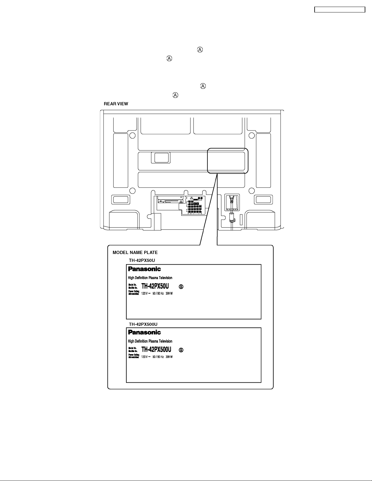
1. Model number is indication in rear cover is only "TH-42PX50U " only in rear cover as shown in figure.
2. TH-42PX50U was discontinued and TH-42PX50U
2.2. TH-42PX500UA
1. Model number is indication in rear cover is only "TH-42PX500U " only in rear cover as shown in figure.
2. TH-42PX500U was discontinued and TH-42PX500U
was introduced from NOV/2005.
was introduced from NOV/2005.
TH-42PX50U / TH-42PX500U
3
TH-42PX50U / TH-42PX500U
3 Adjustment Procedure
3.1. Driver Set-up
3.1.1. Item / Preparation
1. Input a white signal of the RGB signal generator.
2. Set the picture controls: Picture menu: Standard
Color temperature: Middle
Picture: 25
Aspect: Full
Caution
1. First perform Vsus adjustment.
2. Confirmation of Vscn voltage should be performed after
confirmation of Vad adjustment.
When Vad=-90V, Voltage of Vscn is 30V ±3V.
3.1.2. Adjustments
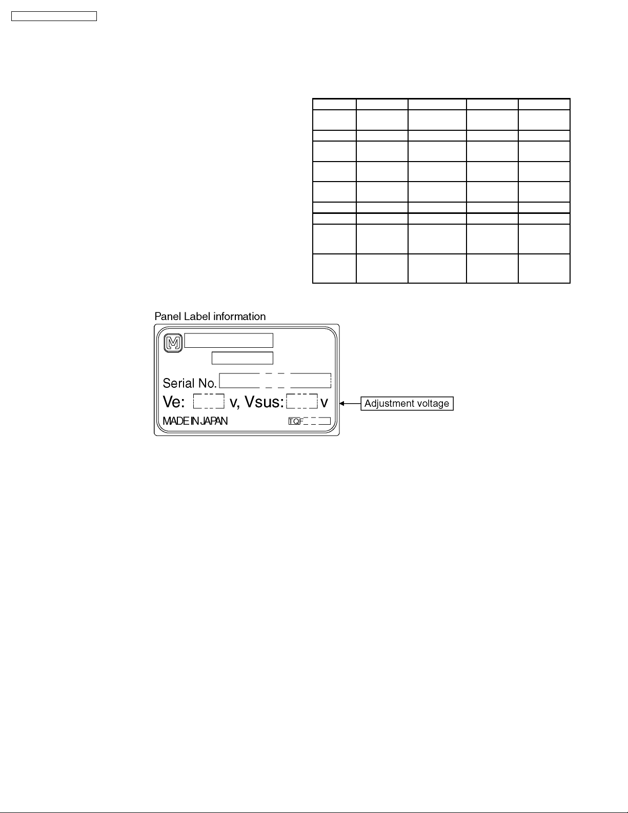
Adjust driver section voltages referring the panel data on the
panel data label.
Name Test Point Voltage Volume Remarks
Vsus TPVSUS
(SS)
Ve TPVE (SS) Ve ± 2V VR6145 (SS) *
Vset TPVSET
(SC)
Vad TPVAD (SC) -105V ± 1V VR6477
Vscn TPVSCN
(SC)
Vda TPVDA (SS) 70V ± 1V VR352 (P)
PFC C446 (+)(-) 395V ± 0.5V R443 (P)
Vlow C555 (+)(-) 73V ± 0.1V R661 (P) Vda load
Csus TPVSUS
(SS)
*See the Panel label.
Vsus ± 2V VR351 (P) *
240V ± 7V Fixed
(SC)
Vad+130V ±4VFixed
current :
0.4A
178V ± 0.5V R671 (P) Vsus load
current :
1.7A
4
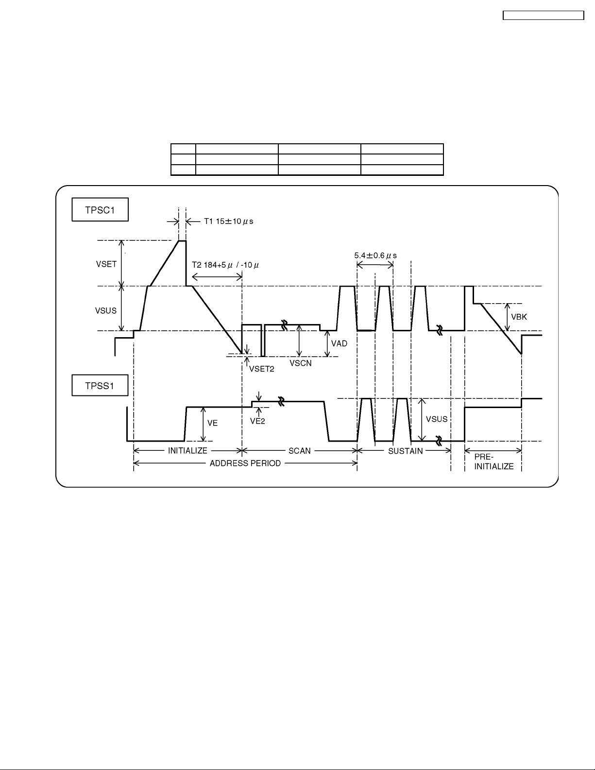
3.2. Initialization Pulse Adjust
1. Input the White signal to plasma video input.
2. Set the picture controls as follows.
· Picture menu: Standard
· Color temperature : Middle
· Picture : 25
3. Connect Oscilloscope to TPSC1 (T1) and check for 15±10µ Sec.
4. Connect Oscilloscope to TPSC1 (T2) and adjust R6557 for 184+5µ /-10µ Sec.
Test point Volume Level
T1 TPSC1 (SC) --- 15 ± 10µ Sec
T2 TPSC1 (SC) R6557 (SC) 184 + 5µ / - 10µ Sec
TH-42PX50U / TH-42PX500U
5

TH-42PX50U / TH-42PX500U
3.3. P.C.B. (Printed Circuit Board) exchange
3.3.1. Caution
1. To remove P.C.B. , wait 1 minute after power was off for discharge from electrolysis capacitors.
3.3.2. Quick adjustment after P.C.B. exchange
P.C.B. Name Test Point Voltage Volume Remarks
P Board Vsus TPVSUS (SS) Vsus ± 2V VR351 (P) *
Vda TPVDA (SS) 70V ± 1V VR352 (P)
PFC C446 (+) (-) (P) 395V ± 0.5V R443 (P)
Vlow C555 (+) (-) (P) 73V ± 0.1V R661 (P) Vda load current : 0.4A
Csus TPVSUS (SS) 178V ± 0.5V R671 (P) Vsus load current : 1.7A
SC Board Vad TPVAD (SC) -105V ± 1V VR6477 (SC)
SS Board Ve TPVE (SS) Ve ± 2V VR6145 (SS) *
D, DG Board White blance, Pedestal and Sub brightness for NTSC, PAL, HD, PC and 625i signals
*See the Panel label.
Caution:
Absolutely do not reduce Vsus below Ve not to damage the P.C.B.
3.4. Adjustment Volume Location
6
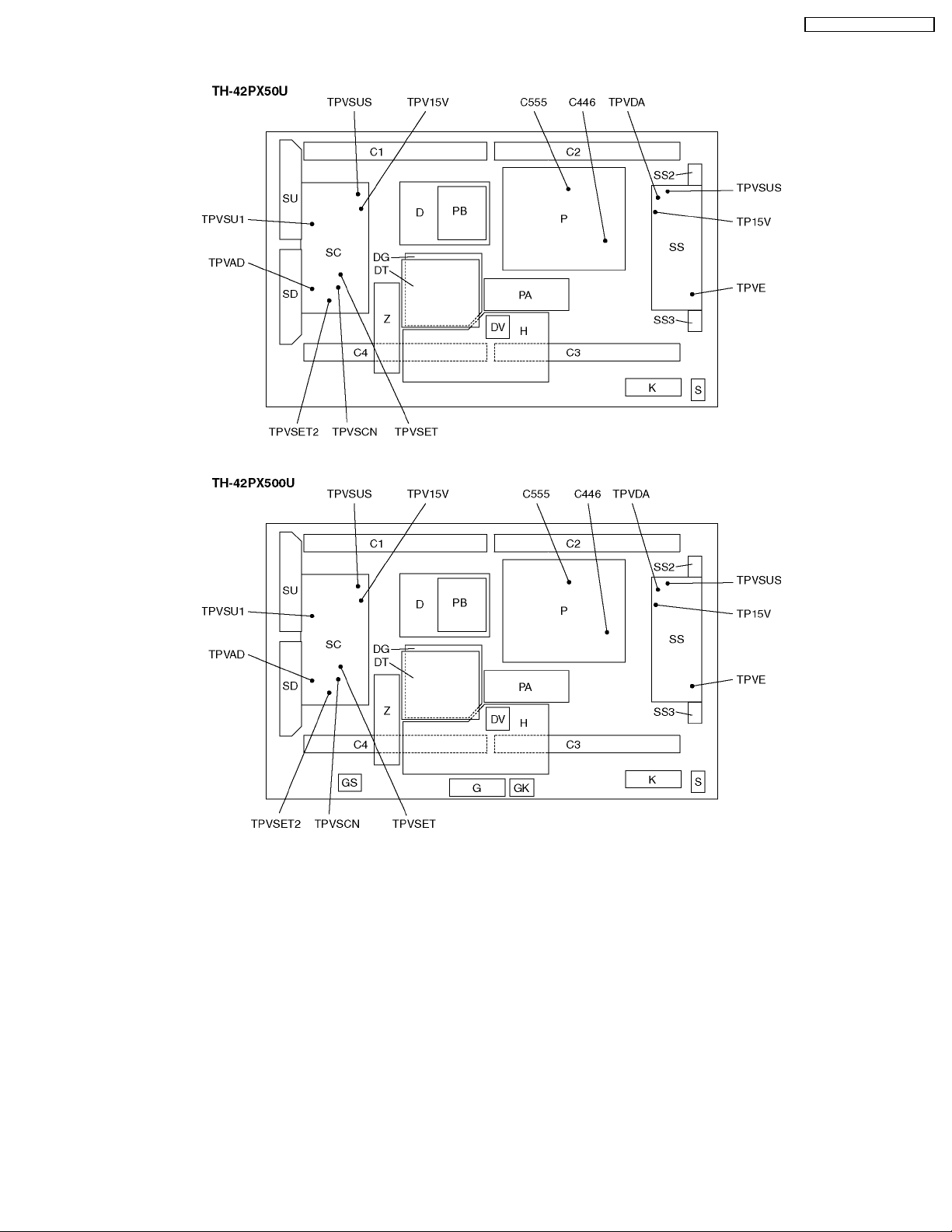
3.5. Test Point Location
TH-42PX50U / TH-42PX500U
7

TH-42PX50U / TH-42PX500U
8